
FILE NO.
REFERENCE No.SM5310776
SG318/U, EX, GX, U2, EX2, GX2, U3, EX3, GX3, U4
NOTE: 1. Parts order must contain model number, part number, and description.
2. Substitute parts may be supplied as the service parts.
3. N.S.P. : Not available as service parts.
Design and specifications are subject to change without notice.
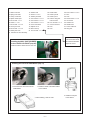
SERVICE MANUAL
CONTENTS
1. OUTLINE OF CIRCUIT DESCRIPTION .....................................3
2. DISASSEMBLY ........................................................................11
3. ELECTRICAL ADJUSTMENT ..................................................19
4. USB STORAGE INFORMATION REGISTRATION ..................24
5. TROUBLESHOOTING GUIDE .................................................25
6. PARTS LIST .............................................................................26
CIRCUIT DIAGRAMS & PRINTED WIRING BOARDS ................C1
RoHS
This product does not contain any hazardous substances prohibited by the
RoHS Directive.
WARNING
You are requested to use RoHS compliant parts for maintenance or repair.
You are requested to use lead-free solder.
(This product has been manufactured using lead-free solder. Be sure to follow
the warning given on page 2 when carrying out repair work.)
CAUTION: Danger of explosion if battery is incorrectly replaced.
Replace only with the same of equivalent type recommended by the
manufacturer.
Discard used batteries according to the manufacturer's instruction.
Design and specifications are subject to change without notice.
VPC-CA9EXBK
(Product Code : 168 177 03)
(Europe)(U.K.)(South America)(China)
(Australia)(Hong Kong)(Russia)(Africa)
(Middle East)(Korea)(Taiwan) (General)
VPC-CA9BK
(Product Code : 168 177 02)
(U.S.A.)(Canada)(Taiwan)
VPC-CA9GXBK
(Product Code : 168 177 04)
(South America)(China)(Australia)
(Hong Kong)(General)(Korea)(Taiwan)
VPC-CA9R
(Product Code : 168 177 06)
(U.S.A.)(Canada)(Taiwan)
VPC-CA9EXR
(Product Code : 168 177 07)
(Europe)(U.K.)(South America)(China)
(Australia)(Hong Kong)(Russia)(Africa)
(Middle East)(Korea)(Taiwan) (General)
VPC-CA9GXR
(Product Code : 168 177 08)
(South America)(China)(Australia)
(Hong Kong)(General)(Korea)(Taiwan)
VPC-CA9G
(Product Code : 168 177 10)
(U.S.A.)(Canada)(Taiwan)
VPC-CA9EXG
(Product Code : 168 177 11)
(Europe)(U.K.)(South America)(China)
(Australia)(Hong Kong)(Russia)(Africa)
(Middle East)(Korea)(Taiwan) (General)
VPC-CA9GXG
(Product Code : 168 177 12)
(South America)(China)(Australia)
(Hong Kong)(General)(Korea)(Taiwan)
VPC-CA9YL
(Product Code : 168 177 13)
(U.S.A.)(Canada)(Taiwan)

- 2 -
WARNING
Do not use solder containing lead.
This product has been manufactured using lead-free
solder in order to help preserve the environment.
Because of this, be sure to use lead-free solder when
carrying out repair work, and never use solder
containing lead.
Lead-free solder has a melting point that is 30 - 40°C (86 -
104°F) higher than solder containing lead, and moreover it
does not contain lead which attaches easily to other metals.
As a result, it does not melt as easily as solder containing
lead, and soldering will be more difficult even if the
temperature of the soldering iron is increased.
The extra difficulty in soldering means that soldering time
will increase and damage to the components or the circuit
board may easily occur.
Because of this, you should use a soldering iron and
solder that satisfy the following conditions when carrying out
repair work.
Soldering iron
Use a soldering iron which is 70 W or equivalent, and
which lets you adjust the tip temperature up to 450°C
(842°F). It should also have as good temperature recovery
characteristics as possible.
Set the temperature to 350°C (662°F) or less for chip
components, to 380°C (716°F) for lead wires and similar,
and to 420°C (788°F) when installing and removing shield
plates.
The tip of the soldering iron should have a C-cut shape or
a driver shape so that it can contact the circuit board as flat
or in a line as much as possible.
Solder
Use solder with the metal content and composition ratio by
weight given in the table below. Do not use solders which
do not meet these conditions.
Lead-free solder is available for purchase as a service tool.
Use the following part number when ordering:
Part name: Lead-free solder with resin (0.5 mm dia., 500 g)
Part number: VJ8-0270
Note:
If replacing existing solder containing lead with lead-free
solder in the soldered parts of products that have been
manufactured up until now, remove all of the existing solder
at those parts before applying the lead-free solder.
The components designated by a symbol ( ! ) in this schematic diagram designates components whose value are of
special significance to product safety. Should any component designated by a symbol need to be replaced, use only the
part designated in the Parts List. Do not deviate from the resistance, wattage, and voltage ratings shown.
PRODUCT SAFETY NOTICE
Metal content Tin (Sn) Silver (Ag) Copper (Cu)
Composition
ratio by weight
96.5% 3.0% 0.5%

- 3 -
1. OUTLINE OF CIRCUIT DESCRIPTION
1-1. CMOS CIRCUIT DESCRIPTION
1. IC Configuration
The CMOS peripheral circuit block basically consists of the
following ICs.
IC911 (MT9J001I12STCV)
CMOS imager
CDS, AGC, ADC built-in
H driver, V driver, serial communication circuit built-in
2. IC911 (CMOS)
[Structure]
The electric charges which are generated when each pixel is
optically converted are in turn converted into signal voltages
by the FD amplifier, and they are then transmitted by the built-
in H driver and V driver. The signals are sampled and ampli-
fied by the CDS and PGA circuits at the point they are output,
and then they are AD converted and output. The output uses
the 12 bit LVDS interface.
1/2.3-inch positive pixel array CMOS-type fixed imaging ele-
ment
Effective pixels 3856 (H) X 2764 (V)

- 4 -
1-2. CP1 and VF1 CIRCUIT DESCRIPTION
1. Circuit Description
1-1. Digital clamp
The optical black section of the image sensor extracts aver-
aged values from the subsequent data to make the black
level of the image sensor output data uniform for each line.
The optical black section of the image sensor averaged value
for each line is taken as the sum of the value for the previous
line multiplied by the coefficient k and the value for the cur-
rent line multiplied by the coefficient 1-k.
1-2. Signal processor
1. gamma correction circuit
This circuit performs (gamma) correction in order to maintain
a linear relationship between the light input to the camera
and the light output from the picture screen.
2. Color generation circuit
This circuit converts the image sensor into RGB signals.
3. Matrix circuit
This circuit generates the Y signals, R-Y signals and B-Y sig-
nals from the RGB signals.
4. Horizontal and vertical aperture circuit
This circuit is used gemerate the aperture signal.
1-3. AE/AWB and AF computing circuit
The AE/AWB carries out computation based on a 64-seg-
ment screen, and the AF carries out computations based on
a 6-segment screen.
1-4. SDRAM controller
This circuit outputs address, RAS, CAS and AS data for con-
trolling the SDRAM. It also refreshes the SDRAM.
1-5. Communication control
1. SIO
This is the interface for the 8-bit microprocessor.
2. PIO/PWM/SIO for LCD
8-bit parallel input and output makes it possible to switch be-
tween individual input/output and PWM input/output.
1-6. TG/SG
Timing generated for image sensor control.
1-7. Digital encorder
It generates chroma signal from color difference signal.
2. Outline of Operation
When the shutter opens, the reset signals (ASIC and CPU)
and the serial signals (“take a picture” commands) from the
8-bit microprocessor are input and operation starts.
When the TG/SG drives the image sensor, picture data passes
through the A/D and CDS, and is then input to the ASIC. The
AF, AE, AWB, shutter, and AGC value are computed from
this data, and exposures are made to obtain the optimum
picture. The data which has already been stored in the
SDRAM is read by the CPU and color generation is carried
out. Each pixel is interpolated from the surrounding data as
being either R, G, and B primary color data to produce R, G
and B data. At this time, correction of the lens distortion which
is a characteristic of wide-angle lenses is carried out. After
AWB and gamma processing are carried out, a matrix is gen-
erated and aperture correction is carried out for the Y signal,
and the data is then compressed by JPEG and is then writ-
ten to card memory (SD card).
When the data is to be output to an external device, it is
taken data from the memory and output via the USB I/F.
When played back on the LCD and monitor, data is trans-
ferred from memery to the SDRAM, and the image is then
elongated so that it is displayed over the SDRAM display
area.
3. LCD Block
The LCD display circuit is located on the CP1 board and VF1
board, and consists of components such as a power circuit
and VCOM control circuit.
The signals from the ASIC are 8-bit digital signals, that is
input to the LCD directly. The 8-bit digital signals are con-
verted to RGB signals inside the LCD driver circuit. The LCD
is input signals from ASIC directly to the LCD, and function
such as image quality are controlled.
Because the LCD closes more as the difference in potential
between the VCOM (common polar voltage: AC) and the R,
G and B signals becomes greater, the display becomes
darker; if the difference in potential is smaller, the element
opens and the LCD become brighter.
In addition, the timing pulses for signals other than the video
signals are also input from the ASIC directory to the LCD.

- 5 -
5. Video Clip Recording and Playback
5-1. Recording
The signals from the camera block are input to the ASIC where
they are processed, and the image data that is stored in the
IC121 SDRAM converts MPEG4 encoded data inside the ASIC,
and the data is then written in sequence onto the SD card. At
this time, the audio signals that are input to the built-in micro-
phone are converted into digital data by the audio CODEC IC
of IC182. The audio data is then encoded (AAC) inside the
ASIC, and is then written in sequence onto the SD card to-
gether with the image signals described above.
5-2. Playback
The data is read from the SD card. The encoded data is de-
coded into image data inside the ASIC and then where it is
displayed by the LCD or on a TV monitor. At this time, the
audio data is also decoded, and it is input to IC182 as digital
data. D/A conversion is carried out at IC182, and the sound is
then output to the speaker or to the LINE OUT terminal.
6. Audio CODEC Circuit (IC182)
The audio signals from the microphone are converted into 16-
bit digital data. AD conversion is carried out at a maximum
sampling frequency of 48 kHz.
During audio playback, the 16-bit digital data is converted into
analog signals and these drive the speaker or line out system.
DA conversion is carried out at a maximum sampling frequency
of 48 kHz.
4. Lens drive block
4-1. Focus drive
The 16-bit serial data signals (LENS_SDI) and (LENS_SCLK
and LENS_EN) which are output from the ASIC (IC101) are
used to drive (FOCUS A +, FOCUS A -, FOCUS B + and FO-
CUS B -) by the motor driver IC (IC951), and are then used to
microstep-drive the stepping motor for focusing operation.
Detection of the focus reference position is carried out by the
photointerruptor (F_SENSE) which is inside the lens block.
4-2. Zoom drive
The 16-bit serial data signals (LENS_SDI) and (LENS_SCLK
and LENS_EN) which are output from the ASIC (IC101) are
used to drive (ZOOM A +, ZOOM A -, ZOOM B + and ZOOM B
-) by the motor driver IC (IC951), and are then used to
microstep-drive the stepping motor for zooming operation.
Detection of the focus reference position is carried out by the
photointerruptor (Z_SENSE) which is inside the lens block.
4-3. ND filter
The 16-bit serial data signals (LENS_SDI) and (LENS_SCLK
and LENS_EN) which are output from the ASIC (IC101) are
used to drive (ND+ and ND-) by the motor driver IC (IC951),
and then the ND filter is inserted into and removed from the
beam path.
4-4. Iris drive
The output from the Hall sensor inside the lens is amplified by
the Hall amplifier circuit inside the IC951 motor drive IC, and
the difference between the current and target aperture deter-
mined by the resulting output and the exposure amout (16 bit
serial signal (LENS_SDI) and (LENS_SCLK and LENS_EN))
output from the ASIC (IC101) is input to the servo amplifier
circuit (IC951) to keep the aperture automatically controlled
(DRIVE+ and DRIVE -) to the target aperture, and drive the
galvanometer.
4-5. Shutter drive
This is carried out by applying reverse voltages to the aperture
driving coil. To operate the shutter, the SHUTTER+ signal
which is output from the ASIC (IC101) is set to a high level
(SHUTTER signals are input to IC951).

- 6 -
1-3. PWA POWER CIRCUIT DESCRIPTION
1. Outline
This is the main power circuit, and is comprised of the follow-
ing blocks.
Switching controller (IC501)
Motor system power output (L5301)
Digital 3.25 V power output (L5002)
Digital and CMOS 1.8 V power output (IC504, L5006)
Backlight power output (Q5007, L5007)
Digital 1.2 V power output (L5003)
CMOS analog 2.8 V power output (IC503, L5005)
2. Switching Controller (IC501)
This is the basic circuit which is necessary for controlling the
power supply for a PWM-type switching regulator, and is pro-
vided with seven built-in channels, only CH1 (motor system),
CH2 (digital 3.25 V), CH3 (digital 1.2 V) and CH7 (backlight)
are used.
Each power supply output is received, and the PWM duty is
varied so that each one is maintained at the correct voltage
setting level.
Feedback for the backlight power (CH7) is provided to the
both ends voltage of registance so that regular current can
be controlled to be current that was setting.
2-1. Short-circuit protection circuit
If output is short-circuited for the length of time determined
by the condenser which is connected to Pin (A6) of IC501, all
output is turned off. To reset, momentarily set the control sig-
nal (P ON) to repeat control, or temporarily disconnect the
input power supply.
3. Motor System Power Output
BOOST 5 V is output. Feedback for the 5.0 V output is pro-
vided to the switching controller (Pin (B7) of IC501) so that
PWM control can be carried out.
4. Digital 3.25 V Power Output
VDD3 is output. Feedback for the VDD3 is provided to the
swiching controller (Pin (F3) of IC501) so that PWM control
can be carried out.
5. Digital 1.8 V and CMOS 1.8 V Power Output
VDD 1.8 and CMOS 1.8 V are output. Feedback for the 1.8 V
is provided to the switching power supply controller (Pin (3)
of IC504) so that PWM control to be carried out.
6. Backlight Power Supply output
Regular current is being transmitted to LED for LCD back-
light. Feedback for the both ends voltage of registance that
is being positioned to in series LED are provided to the switch-
ing controller (Pin (C4) of IC501) so that PWM control to be
carried out.
7. Digital 1.2 V Power Output
VDD 1.2 is output. Feedback for the VDD 1.2 is provided to
the switching controller (Pin (C3) of IC501) so that PWM con-
trol to be carried out.
8. CMOS Analog 2.8 V Power Output
VAA 2.8 is output. Feedback for the VAA 2.8 is provided to
the switching power supply controller (Pin (3) of IC503) so
that PWM control to be carried out.

- 7 -
1-4. ST1 STROBE CIRCUIT DESCRIPTION
1. Charging Circuit
When UNREG power is supplied to the charge circuit and
the CHG signal from microprocessor becomes High (3.3 V),
the charging circuit starts operating and the main electorolytic
capacitor is charged with high-voltage direct current.
However, when the CHG signal is Low (0 V), the charging
circuit does not operate.
1-1. Charge switch
When the CHG signal switches to Hi, IC541 starts charging
operation.
1-2. Power supply filter
C5401 constitutes the power supply filter. They smooth out
ripples in the current which accompany the switching of the
oscillation transformer.
1-3. Oscillation circuit
This circuit generates an AC voltage (pulse) in order to in-
crease the UNREG power supply voltage when drops in cur-
rent occur. This circuit generates a drive pulse with a fre-
quency of approximately 200-300 kHz, and drive the oscilla-
tion transformer.
1-4. Oscillation transformer
The low-voltage alternating current which is generated by the
oscillation control circuit is converted to a high-voltage alter-
nating current by the oscillation transformer.
1-5. Rectifier circuit
The high-voltage alternating current which is generated at
the secondary side of T5401 is rectified to produce a high-
voltage direct current and is accumulated at electrolytic ca-
pacitor C5412.
1-6. Charge monitoring circuit
The functions programmed in the IC541 monitor oscillations
and estimate the charging voltage. If the voltage exceeds the
rated value, charging automatically stops. Then, the
ZCHG_DONE signal is changed to Lo output and a "charg-
ing stopped" signal is sent to the microcomputer.
2. Light Emission Circuit
When FLCTL signal is input from the ASIC, the stroboscope
emits light.
2-1. Emission control circuit
When the FLCLT signal is input to the emission control cir-
cuit, Q5402 switches on and preparation is made to the light
emitting. Moreover, when a FLCLT signal becomes Lo, the
stroboscope stops emitting light.
2-2. Trigger circuit
The Q5402 is turned ON by the FLCLT signal and light emis-
sion preparation is preformed. Simultaneously, high voltage
pulses of several kV are emitted from the trigger coil and
applied to the light emitter.
2-3. Light emitting element
When the high-voltage pulse form the trigger circuit is ap-
plied to the light emitting part, currnet flows to the light emit-
ting element and light is emitted.
Beware of electric shocks.

- 8 -
See next page
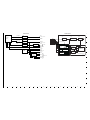
1-5. SYA CIRCUIT DESCRIPTION
1. Configuration and Functions
For the overall configuration of the SYA block, refer to the block diagram. The SYA block centers around a 8-bit microprocessor
(IC301), and controls camera system condition (mode).
The 8-bit microprocessor handles the following functions.
1. Operation key input, 2. Clock control and backup, 3. Power ON/OFF, 4. Storobe charge control
Pin
Signal
ASIC_SCK
PON2
CL
POW_TEST
HOT LINE
TEST
CL
LCDPWM
VDD2
ST_CHG
ZCHGDONE
ONENAND RESET
ZBACKUPCTL
KEY_PLAY
GREEN_LED
MRST
UTX
RTX
KEY_VREC
KEY_POWER
ZBOOT_COMREQ
NOT USED
NOT USED
NOT USED
VSS3
VDD3
RDSEL
CLK (SFW)
DATA0 (SFW)
P ON
I/O
Outline
TO Asic
Test mode
Correspondence from ASIC
Test mode
CL
-
Strobe charge control (H= charge)
Main condensor charge voltage detection
OneNAND flash reset
Backup circuit (L=ON)
L: Key detection PLAY
System reset (L=reset)
Battery residual quantity ICTXD: Debugger
Key detection VREC (L= detection)
L: InterruptKey. Key detection POWER
BOOT low output
-
-
-
-
-
Debugger terminal
Debugger terminal
Debugger terminal
PWA DIGITAL
Battery residual quantity ICRXD
VSS2 -
MR_OPEN L: Panel close
KEY_MENU Key detection MENU (L= detection)
LCD backlight brightness control
KEY_1st L: InterruptKey. Key detection shutter
KEY_SET Key detection SET (L= detection)
KEY_UP Key detection UP (L= detection)
KEY_DOWN Key detection DOWN (L= detection)
KEY_LEFT Key detection LEFT (L= detection)
KEY_RIGHT Key detection RIGHT (L= detection)
NOT USED -
SW3.2ON SW 3.2V supply (L= ON)
O
O
O
I
I
I
O
O
-
-
O
I
O
O
I
O
O
O
O
I
I
I
I
I
I
I/O
-
-
I
I
I
I
I
-
-
-
-
-
-
O
-
O
1
2
3
4
5
6
7
8
9
10
11
12
13
14
15
16
17
18
19
20
21
22
23
24
25
26
27
28
29
30
31
32
33
34
35
36
37
38
39
40
41
42
PWA DIGITAL
CL
Green LED
RED_LED
SW unit LED (H= lighting)

- 9 -
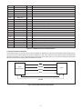
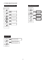
Fig. 5-1 Internal Bus Communication System
2. Internal Communication Bus
The SYA block carries out overall control of camera operation by detecting the input from the keyboard and the condition of the
camera circuits. The 8-bit microprocessor reads the signals from each sensor element as input data and outputs this data to the
camera circuits (ASIC) or to the LCD display device as operation mode setting data. Fig. 5-1 shows the internal communication
between the 8-bit microprocessor, ASIC and SPARC lite circuits.
Table 5-1. 8-bit Microprocessor Port Specification
-
ZAVJACK
AV JACK connection detection for three value detection
VSS1
UNREG SY
Power supply voltage measurement of 1/2UNREGSY
NOT USED -
VDD1
-
KEY_2ND
L: InterruptKey. Key detection shutter
ZUSBDET
USB detection (L= detection)
RESET SBM reset (L= reset)
XCIN 32K oscillation input terminal
XCOUT 32K oscillation output terminal
NOT USED
-
8-bit
Microprocessor
ASIC
SREQ
ASIC SO
ASIC SI
SCK
MRST
ZBAT_OFF
CL
NOT USED
NOT USED
AD INPUT OK
-
-
L: Interruption. From power supply watch IC
L: Interruption. Correspondence from ASIC
SREQ
HINGE
LCD panel rotation detection (L= panel inversion)
ZCARD
Card detection (L= detection)
TH_TEMP
Camera temperature detection
ASIC_SDI
Data output toASIC
ASIC_SDO
Data input from ASIC
PLLEN
43
44
45
46
47
48
49
50
51
52
53
54
55
56
57
58
59
60
61
62
63
64
O
I
I
O
-
-
I
I
I
I
I
I
O
-
-
-
-
I
I
I
O
I
PLLEN EV3X PLLEN

- 10 -
ASIC,
memory
CMOS
8 bit CPU
Power voltage
Power OFF
Play back
LCD finder
3.3 V 1.8 V 1.0 V
1.8 V 2.8 V (A)
3.2 V
OFF
OFF
32KHz
OFF
OFF
32KHz
ON
ON
4 MHz
ON
OFF
4 MHz
Table 5-2. Camera Mode
Note) 4 MHz = Main clock operation, 32 kHz = Sub clock operation
3. Power Supply Control
The 8-bit microprocessor controls the power supply for the overall system.
The following is a description of how the power supply is turned on and off. When the battery is attached, a regulated 3.2 V
(power off: 2.4 V) voltage is normally input to the 8-bit microprocessor (IC301) by IC302, so that clock counting and key scan-
ning is carried out even when the power switch is turned off, so that the camera can start up again. When the battery is removed,
the 8-bit microprocessor operates in sleep mode using the backup battery. At this time, the 8-bit microprocessor only carries out
clock counting, and waits in standby for the battery to be attached again. When a switch is operated, the 8-bit microprocessor
supplies power to the system as required.
The 8-bit microprocessor first set the P ON signal at pin (40) to high, and then turns on the DC/DC converter. After this, low
signal is output from pin (17) so that the ASIC is set to the reset condition. After this these pins set to high, and set to active
condition. Once it is completed, the ASIC returns to the reset condition, all DC/DC converters are turned off and the power
supply to the whole system is halted.
Power switch ON - Auto power OFF
CAMERA
LCD
MONITOR
3.3 V 7V
OFF
OFF
ON
ON

- 11 -
2. DISASSEMBLY
Note:
1. When disassembling and reassembling the main unit, the LCD and the battery cover, always be sure to use the air
leak tester (VJ8-0303) to test for air leaks and to check that the waterproof mechanism is functioning normally.
Refer to the Instruction Manual provided with the air leak test tool for details on how to carry out the air leak test.
2. This camera uses waterproof packing. It is recommended that you replace the waterproof packing approximately
once every year. The waterproof packing is supplied in the COMPL, MENT KIT-SV-114 (P/No. 636 110 2131) shown
in the table below. These parts can also be supplied as single parts.
Summary of waterproof maintenance parts kit
Parts name: COMPL, MENT KIT-SV-114
Parts code: 636 110 2131
NO. DESCRIPTION
1
2
3
4
5
6
7
GASKET CABINET-SG114/J
vSPACER MIC2-SG114/J
GASKET LCD-SG114/J
PAD BATTERY-SG114/J
ADHESIVE COV BATT A-SG114
ADHESIVE COV BATT B-SG114
ADHESIVE COV BATT D-SG114
NUMBER
PAD BATTERY-SG114/J
ADHESIVE COV BATT A-SG114
CABINET
LCD
COVER
BATTERY
PARTS NO.
636 104 0174
636 107 3998
636 104 0181
636 104 0198
636 104 7173
636 104 7180
636 106 6044
GASKET CABINET-SG114/J
GASKET LCD-SG114/J
PAD BATTERY-SG114/J
ADHESIVE COV BATT A-SG114
SPACER MIC2-SG114/J
ADHESIVE COV BATT D-SG114
ADHESIVE COV BATT B-SG114
When doing an air leak test at the
LCD, these parts must be replaced.
(If these parts are not removed, it
will not be possible to do the air leak
test at the LCD.)
SECTION
List of waterproof maintenance parts kit
1
2
1
1
1
1
1

- 12 -
A
J
K
J
K
M
1
2
3
6
7
8
5
11
11
6
d
a
c
e
b
A
B
D
10
4
12
13
9
f
14
15
16
B
A
C
17
18
19
21
22
27
28
29
30
a
b
c
32
33
11
C
E
25
31
23
20
24
26
31
31
P
P
Q
Q
NOTE: Discharge a strobe capacitor
with the discharge jig (VJ8-0188) for
electric shock prevention.
When assembling,
tighten the screws order.
a b c d e f
When assembling,
assemble order.
A B C
When assembling,
assemble order.
A
B C D E
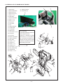
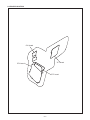
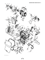
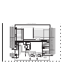
2-1. REMOVAL OF CABI LEFT AND LENS
When assembling,
assemble order.
a b c

- 13 -
1. Screw 1.7 x 2.5
2. Screw 1.7 x 3.5
3. Cover joint base
4. Open the cover battery.
5. Screw 1.4 x 2.5
6. Five screws 1.7 x 5
7. Dec grip
8. Button menu
9. Screw 1.7 x 5
10. Screw 1.7 x 3.5
11. Four screws 1.7 x 4.5
12. Cabinet left
13. Gasket cabinet
14. Two screws 1.7 x 2.5
15. Screw 1.7 x 5
16. Heat sink ASIC
17. Spacer power
18. FPC
19. Spacer CA1
20. Spacer CA1 PWB
21. Spacer ST1 wire
22. Remove the solder.
23. Heat sink rubber left
24. Screw 1.7 x 4.5
25. Screw 1.4 x 4
26. Holder lens
27. Connector
28. FPC
29. FPC
30. Lens assy
31. Three screws 1.4 x 4.5
32. Heat sink CMOS
33. Assy, flexible pwb CA1
When reassembling
The air leak test should
be carried out between
steps 8 and 9.
At this time, the battery
cover should be closed
and locked.
approximately
90 degrees
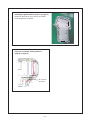
ASSY, FPC GASKET installing method
(between steps 8 and 9 on page 12 and 13)
Tilt the LCD to approximately 90 degrees.
Next, push the ASSY, FPC GASKET gently with a
finger until the clearance t between the bottom
CABINET RIGHT edge of the ASSY, FPC GAS-
KET and the CABINET RIGHT is 0.
t
ASSY, FPC GASKET
CABINET RIGHT
t=0
ASSY, FPC GASKET
Push until t=0, T=0
T=0
ASSY, FPC GASKET
T
Bend at 90 ± 10°
(LCD is closed)
Bend gently
(LCD is closed)

- 14 -
1
2
5
4
6
7
8
9
3
10
11
12
13
14
Installing the gasket cabinet (step 13 on page 12)
Install from directly above in the order of the numbers
so that the gasket is not twisted.
Do not touch
the solder.
Lead wire of speaker dressing method
(step 22 on page 12)

- 15 -
1
2
5
6
20
21
22
7
9
10
11
23
15
16
17
18
19
25
26
24
3
4
12
13
14
27
28
29
31
32
8
30
B
B
A
I
L
I
L
N
N
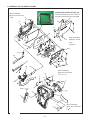
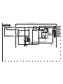
2-2. REMOVAL OF CP1 BOARD AND ST1 BOARD
1. Spacer flash
2. Spacer holder flash
3. Spacer lens unit
4. Spacer lens unit 2
5. Screw 1.7 x 4
6. Holder flash
7. Remove the solder.
8. Screw 1.7 x 4
9. Screw 1.7 x 4
10. Earth joint
11. CP1 board
12. FPC
13. Spring batt eject
14. Terminal batt
15. Cover triger
16. Spacer ST1
17. Two screws 1.7 x 2
18. Connector
19. ST1 board
20. Remove the solder.
21. Spacer H flash B
22. Assy, lamp
23. Screw 1.7 x 2
24. Holder CP1
25. Screw 1.7 x 2
26. Holder CP1 2
27. Two screws 1.7 x 6
28. Assy, holder strap
29. Gasket strap
30. Screw 1.7 x 3.5
16
3
4
1
31. Spring lock lever
32. Lever batt lock
When assembling
The air leak test should be carried out
between steps 26 and 27.
At this time, 12. Cabi left, 13 Gasket
cabinet and 9, 10, 11 six screws on
page 12 should be assembled to the
main body, and carry out the air leak
test. When the air leak test is finished,
disassembling above parts.

- 16 -
1
2
3
31
32
33
34
35
36
37
38
B
A
B
A
c
b
a
d
A
A
C
C
19
4
5
5
6
7
8
9
10
11
12
13
14
15
15
16
17
18
20
21
21
22
22
23
24
25
26
27
28
29
30
30
4
B
A
d
A
B
C
c
b
a
d
E
G
E
D
D
C
C
F
H
G
F
M
H
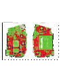
2-3. REMOVAL OF LCD AND VF1 BOARD
When assembling,
tighten the screws
order.
A B C
When assembling,
tighten the screws order.
a
b c d
When assembling,
tighten the screws order.
A
B
Installing the gasket LCD (step 36)
Install from directly above in the order of
the numbers so that the FPC is not twisted.
When assembling,
tighten the screws order.
A
B

- 17 -
1. Shaft cover batt
2. Spring cover batt
3. Compl, cover batt
4. Spacer holder joint
5. Two screws 1.7 x 4
6. Screw 1.7 x 2.5
7. Two screws 1.7 x 3.5
8. Cover joint inner
9. Two screws 1.7 x 3.5
10. Earth joint LCD
11. Pull the LCD from the body.
12. Holder LCD
13. Screw 1.7 x 3.5
14. Holder joint base
15. Two screws 1.7 x 2.5
16. Two screws 1.7 x 3.5
17. Two screws 1.7 x 4.5
18. Cover LCD back
19. Spacer mic 2
20. Dec LCD top
21. Four screws 1.7 x 2
22. Earth LCD A
23. Holder joint R
24. Holder joint L
25. Pull the assy joint
from the LCD.
26. Four screws 1.7 x 3
27. Cover LCD inner
28. FPC
29. FPC
30. Four screws 1.7 x 2.5
31. FPC
32. LCD
33. Three screws 1.7 x 2
34. VF1 board
35. Holder LCD
36. Gasket LCD
37. Cover LCD front
38. Assy joint
Installing the ASSY JOINT (RUBBER)
to the COVER LCD FRONT (step 28)
Install so that the rubber will not come out.
Installing the LCD to the CABI RIGHT (step 11)
1. Insert the FPC of the LCD into the
CABI RIGHT.
2. Install the rubber of the ASSY JOINT
to the cabinet.
3. Install the LCD joint
to the cabinet.
4. After installing, close the LCD.
When reassembling
The air leak test should
be carried out between
steps 20 and 21.

- 18 -
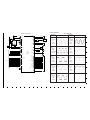
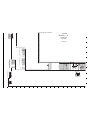
CA1 board
CP1 board
ST1 board
VF1 board
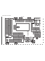
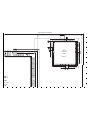
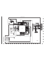
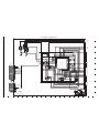
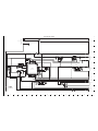
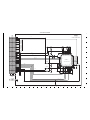
2-4. BOARD LOCATION

- 19 -
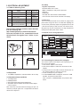
3. ELECTRICAL ADJUSTMENT
3-1. Table for Servicing Tools
Download the calibration software and the firmware
from the following URL.
http://www.digital-sanyo.com/overseas/service/
Place the DscCalDi.exe file, camapi32.dll file and
QrCodeInfo.dll file together into a folder of your
choice.
3-2. Equipment
1. PC (IBM®-compatible PC, Windows 2000 or XP or Vista)
3-3. Adjustment Items and Order
1. Lens Adjustment
2. AWB Adjustment
3. CCD White Point Defect Detect Adjustment
4. CCD Black Point And White Point Defect Detect Adjust-
ment In Lighted
Note: If the lens, CCD and board and changing the part, it is
necessary to adjust again. Item 1-4 adjustments should be
carried out in sequence.
3-4. Setup
1. System requirements
Windows 2000 or XP or Vista
IBM® -compatible PC with pentium processor
USB port
40 MB RAM
Hard disk drive with at least 15 MB available
VGA or SVGA monitor with at least 256-color display
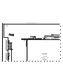
2. Pattern box
Turn on the switch and wait for 30 minutes for aging to take
place before using Color Pure. It is used after adjusting the
chroma meter (VJ8-0192) adjust color temperature to 3100
± 20 K and luminosity to 900 ± 20 cd/m
2
. Be careful of han-
dling the lump and its circumference are high temperature
during use and after power off for a while.
3. Computer screen during adjustment
3-5. Connecting the camera to the computer
This camera requires a DC adaptor (sold separately) in or-
der to use an AC adaptor.
1. Insert the DC adaptor to the camera.
2. Insert the AC adaptor’s cable to DC terminal of the DC
adaptor.
3. Line up the arrow on the cable connector with the notch on
the camera's USB port. Insert the connector.
4. Locate a USB port on your computer.
5. If “USB CONNECTION” is displayed, choose the “COM
PUTER”, and press the SET button.
Next, choose the “CARD READER”, and press the SET
button.
Ref. No.
Name
Part code
J-1
J-2
J-3
J-4
J-5
J-6
J-7
VJ8-0190
VJ8-0192
VJ8-0191
VJ8-0188
VJ8-0260
VJ8-0282
Pattern box
Calibration software
Chroma meter
Spare lump (pattern box)
Discharge jig
Collimator
Spare lump (collimator)
Number
1
1
1
1
1
1
1
J-1 J-3
J-4
J-5
Firmware
Data
AWB
Focus
UV Matrix
R Bright
RGB Offset
Tint
B Bright
Gain
Phase
LCD
Calibration
Upload
PAF Cal.
LCD Type
H AFC Test
VCOMDC
VCOMPP
Cal Data
Cal Mode
OK
OK
EVF
USB storage
Get
Set
VID
Set
PID
Set
Serial
Set
Rev.
Set
Setting
Language
Video Mode
VCO
Factory Code
Hall Cal.
Backrush pulse :
Set
Get

- 20 -
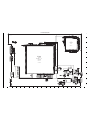
3-8. Adjust Specifications
1. Lens Adjustment
Preparation:
POWER switch: ON
If using a ready-made collimator, set to infinity.
Note:
Do not vibrate during the adjustment.
Adjustment method:
1. Set a distance of 0.5-1.0 cm between camera lens and
collimator lens. Do not touch the each lens.
2. Set the camera so that it becomes center of the screen in
the collimator .
3. Double-click on the DscCalDi.exe.
4. Click the Focus, and click the Yes.
5. Lens infinity adjustment value will appear on the screen.
6. Click the OK.
3-6. The adjustment item which in necessary in part exchange
Factory
Cord
Setting
Language
Setting
Reset
Setting
Lens
Adjust-
ment
AWB
Adjust-
ment
USB
storage
information
registration
CCD White
Point
Defect
Detect
Adjustment
CCD Black
Point And
White Point
Defect
Detect
Adjustment
In Lighted
3-7. Updating the firmware
Check the firmware version immediately after the CP1 board has been replaced. If an old version is being used, interfer-
ence and errors in operation may also occur. If an old version is being used, update it with a newer version.
Refer to
3-13. Firmware uploading procedure. (Page 23)
COMPL PWB CP1
COMPL PWB VF1
COMPL PWB ST1
ASSY, FLEXIBLE PWB CA1
LENS ASSY
Camera
Collimator
: Be sure to carry out the necessary adjustments after replacing the unit.
: Adjustment is possible from the menu setting screen of the camera and by using the calibration software.
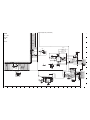
Dsc Calibration
x
OK
Focus Result
STD_AFPOS= 1881
FOCUS= -5,7,14,16
ADJ_PZPOS= 7
LENS_ERR= 0
IRIS_GAIN: -103
IRIS_OFFSET: -27
Page is loading ...
Page is loading ...
Page is loading ...
Page is loading ...
Page is loading ...
Page is loading ...
Page is loading ...
Page is loading ...
Page is loading ...
Page is loading ...
Page is loading ...
Page is loading ...
Page is loading ...
Page is loading ...
Page is loading ...
Page is loading ...
Page is loading ...
Page is loading ...
Page is loading ...
Page is loading ...
Page is loading ...
Page is loading ...
Page is loading ...
Page is loading ...
Page is loading ...
Page is loading ...
Page is loading ...
Page is loading ...
Page is loading ...
Page is loading ...
Page is loading ...
Page is loading ...
Page is loading ...
Page is loading ...
Page is loading ...
Page is loading ...
Page is loading ...
-
 1
1
-
 2
2
-
 3
3
-
 4
4
-
 5
5
-
 6
6
-
 7
7
-
 8
8
-
 9
9
-
 10
10
-
 11
11
-
 12
12
-
 13
13
-
 14
14
-
 15
15
-
 16
16
-
 17
17
-
 18
18
-
 19
19
-
 20
20
-
 21
21
-
 22
22
-
 23
23
-
 24
24
-
 25
25
-
 26
26
-
 27
27
-
 28
28
-
 29
29
-
 30
30
-
 31
31
-
 32
32
-
 33
33
-
 34
34
-
 35
35
-
 36
36
-
 37
37
-
 38
38
-
 39
39
-
 40
40
-
 41
41
-
 42
42
-
 43
43
-
 44
44
-
 45
45
-
 46
46
-
 47
47
-
 48
48
-
 49
49
-
 50
50
-
 51
51
-
 52
52
-
 53
53
-
 54
54
-
 55
55
-
 56
56
-
 57
57


Sanyo VPC-CA9EXG User manual
- Type
- User manual
- This manual is also suitable for
Ask a question and I''ll find the answer in the document
Finding information in a document is now easier with AI
Related papers
-
Sanyo VPC-CG11PXOR User manual
-
Sanyo VPC-CA8GXBK User manual
-
Sanyo VAR-G7U User manual
-
-
-
-
-
-
-
Other documents
-
FSR PWB-320XL-AC4 Installation guide
-
Zephyr ZRE-M90ABSGG 36 Inch Ravenna Island Hood Installation guide
-
BBK DV311S User manual
-
Melissa Hot Beverage Maker 645-078 User manual
-
Zephyr ZRE-E42ABSGG Owner's manual
-
Sharp 00ZFO3MKCUSME User manual
-
Omega OM-NET-1608 Owner's manual
-
-
 Trisa Electronics 9454.0145 Datasheet
-
Extron P/2 DA8 User manual
