Analog Devices ADSP-2181 User manual
- Category
- Networking
- Type
- User manual
This manual is also suitable for

FUNCTIONAL BLOCK DIAGRAM
a
DSP Microcomputers
ADSP-2181/ADSP-2183
FEATURES
PERFORMANCE
30 ns Instruction Cycle Time @ 5.0 Volts
33 MIPS Sustained Performance
34.7 ns Instruction Cycle Time @ 3.3 Volts
Single-Cycle Instruction Execution
Single-Cycle Context Switch
3-Bus Architecture Allows Dual Operand Fetches in
Every Instruction Cycle
Multifunction Instructions
Power-Down Mode Featuring Low CMOS Standby
Power Dissipation with 100 Cycle Recovery from
Power-Down Condition
Low Power Dissipation in Idle Mode
INTEGRATION
ADSP-2100 Family Code Compatible, with Instruction
Set Extensions
80K Bytes of On-Chip RAM, Configured as
16K Words On-Chip Program Memory RAM
16K Words On-Chip Data Memory RAM
Dual Purpose Program Memory for Both Instruction
and Data Storage
Independent ALU, Multiplier/Accumulator, & Barrel
Shifter Computational Units
Two Independent Data Address Generators
Powerful Program Sequencer Provides
Zero Overhead Looping
Conditional Instruction Execution
Programmable 16-Bit Interval Timer with Prescaler
128-Lead TQFP/128-Lead PQFP
SYSTEM INTERFACE
16-Bit Internal DMA Port for High Speed Access to
On-Chip Memory
4 MByte Memory Interface for Storage of Data Tables &
Program Overlays
8-Bit DMA to Byte Memory for Transparent
Program and Data Memory Transfers
I/O Memory Interface with 2048 Locations Supports
Parallel Peripherals
Programmable Memory Strobe & Separate I/O Memory
Space Permits “Glueless” System Design
Programmable Wait State Generation
Two Double-Buffered Serial Ports with Companding
Hardware and Automatic Data Buffering
Automatic Booting of On-Chip Program Memory from
Byte-Wide External Memory, e.g., EPROM, or
Through Internal DMA Port
Six External Interrupts
13 Programmable Flag Pins Provide Flexible System
Signaling
ICE-Port™ Emulator Interface Supports Debugging
in Final Systems
REV. 0
Information furnished by Analog Devices is believed to be accurate and
reliable. However, no responsibility is assumed by Analog Devices for its
use, nor for any infringements of patents or other rights of third parties
which may result from its use. No license is granted by implication or
otherwise under any patent or patent rights of Analog Devices.
ICE-Port is a trademark of Analog Devices, Inc.
© Analog Devices, Inc., 1996
One Technology Way, P.O. Box 9106, Norwood, MA 02062-9106, U.S.A.
Tel: 617/329-4700 Fax: 617/326-8703
GENERAL DESCRIPTION
The ADSP-2181/ADSP-2183 is a single-chip microcomputer
optimized for digital signal processing (DSP) and other high
speed numeric processing applications.
The ADSP-2181/ADSP-2183 combines the ADSP-2100 family
base architecture (three computational units, data address gen-
erators and a program sequencer) with two serial ports, a 16-bit
internal DMA port, a byte DMA port, a programmable timer,
Flag I/O, extensive interrupt capabilities, and on-chip program
and data memory.
The ADSP-2181/ADSP-2183 integrates 80K bytes of on-chip
memory configured as 16K words (24-bit) of program RAM,
and 16K words (16-bit) of data RAM. Power down circuitry is
also provided to meet the low power needs of battery operated
portable equipment. The ADSP-2181 is available in 128-pin
TQFP and 128-pin PQFP packages; the ADSP-2183 is avail-
able in the TQFP package only.
In addition, the ADSP-2181/ADSP-2183 supports new instruc-
tions, which include bit manipulations—bit set, bit clear, bit toggle,
bit test—new ALU constants, new multiplication instruction
(x squared), biased rounding, result free ALU operations, I/O memory
transfers, and global interrupt masking, for increased flexibility.
Fabricated in a high speed, double metal, low power, 0.5 µm
CMOS process, the ADSP-2181 operates with a 30 ns instruc-
tion cycle time (34.7 ns for the ADSP-2183). Every instruction
can execute in a single processor cycle.
The ADSP-2181/ADSP-2183’s flexible architecture and com-
prehensive instruction set allow the processor to perform multiple
operations in parallel. In one processor cycle the ADSP-2181/
ADSP-2183 can:
• generate the next program address
• fetch the next instruction
• perform one or two data moves
• update one or two data address pointers
• perform a computational operation
SERIAL PORTS
MEMORY
FLAGS
PROGRAMMABLE
I/O
BYTE DMA
CONTROLLER
PROGRAM
MEMORY
DATA
MEMORY
EXTERNAL
ADDRESS
BUS
EXTERNAL
DATA
BUS
DMA
BUS
INTERNAL
DMA
PORT
TIMER
SPORT 1SPORT 0
ADSP-2100 BASE
ARCHITECTURE
SHIFTER
MAC
ALU
ARITHMETIC UNITS
POWERDOWN
CONTROL
PROGRAM
SEQUENCER
DAG 0
DAG 1
DATA ADDRESS
GENERATORS
PROGRAM MEMORY ADDRESS
DATA MEMORY ADDRESS
PROGRAM MEMORY DATA
DATA MEMORY DATA

ADSP-2181/ADSP-2183
REV. 0
–2–
This takes place while the processor continues to:
• receive and transmit data through the two serial ports
• receive and/or transmit data through the internal DMA port
• receive and/or transmit data through the byte DMA port
• decrement timer
Development System
The ADSP-2100 Family Development Software, a complete set of
tools for software and hardware system development, supports the
ADSP-2181/ADSP-2183. The System Builder provides a high
level method for defining the architecture of systems under devel-
opment. The Assembler has an algebraic syntax that is easy to
program and debug. The Linker combines object files into an
executable file. The Simulator provides an interactive instruc-
tion-level simulation with a reconfigurable user interface to dis-
play different portions of the hardware environment. A PROM
Splitter generates PROM programmer compatible files. The C
Compiler, based on the Free Software Foundation’s GNU C
Compiler, generates ADSP-2181/ADSP-2183 assembly source
code. The source code debugger allows programs to be corrected
in the C environment. The Runtime Library includes over 100
ANSI-standard mathematical and DSP-specific functions.
The EZ-KIT Lite is a hardware/software kit offering a complete
development environment for the entire ADSP-21xx family: an
ADSP-2181 based evaluation board with PC monitor software
plus Assembler, Linker, Simulator, and PROM Splitter software.
The ADSP-2181 EZ-KIT Lite is a low cost, easy to use hardware
platform on which you can quickly get started with your DSP soft-
ware design. The EZ-KIT Lite includes the following features:
• 33 MHz ADSP-2181
• Full 16-bit Stereo Audio I/O with AD1847 SoundPort®
Codec
• RS-232 Interface to PC with Windows 3.1 Control Software
• Stand-Alone Operation with Socketed EPROM
• EZ-ICE Connector for Emulator Control
• DSP Demo Programs
The ADSP-2181 EZ-ICE
®
Emulator aids in the hardware de-
bugging of ADSP-2181 system. The emulator consists of hard-
ware, host computer resident software, and the target board
connector. The ADSP-2181/ADSP-2183 integrates on-chip
emulation support with a 14-pin ICE-Port interface. This inter-
face provides a simpler target board connection that requires
fewer mechanical clearance considerations than other
ADSP-2100 Family EZ-ICEs. The ADSP-2181/ADSP-2183
device need not be removed from the target system when using
the EZ-ICE, nor are any adapters needed. Due to the small
footprint of the EZ-ICE connector, emulation can be supported
in final board designs.
The EZ-ICE performs a full range of functions, including:
• Stand-alone or in-target operation
• Up to 20 breakpoints
• Single-step or full-speed operation
• Registers and memory values can be examined and altered
• PC upload and download functions
• Instruction-level emulation of program booting and execution
• Complete assembly and disassembly of instructions
• C source-level debugging
See “Designing An EZ-ICE-Compatible Target System” in the
ADSP-2100 Family EZ-Tools Manual as well as page 11 of this
data sheet for exact specifications of the EZ-ICE target board
connector.
Additional Information
This data sheet provides a general overview of ADSP-2181/
ADSP-2183 functionality. For additional information on the
architecture and instruction set of the processor, refer to the
ADSP-2100 Family User’s Manual. For more information about
the development tools, refer to the ADSP-2100 Family Develop-
ment Tools Data Sheet.
ARCHITECTURE OVERVIEW
The ADSP-2181/ADSP-2183 instruction set provides flexible
data moves and multifunction (one or two data moves with a
computation) instructions. Every instruction can be executed in
a single processor cycle. The ADSP-2181/ADSP-2183 assembly
language uses an algebraic syntax for ease of coding and read-
ability. A comprehensive set of development tools supports pro-
gram development.
Figure 1 is an overall block diagram of the ADSP-2181/ADSP-
2183. The processor contains three independent computational
units: the ALU, the multiplier/accumulator (MAC) and the
shifter. The computational units process 16-bit data directly and
have provisions to support multiprecision computations. The
ALU performs a standard set of arithmetic and logic operations;
division primitives are also supported. The MAC performs
single-cycle multiply, multiply/add and multiply/subtract opera-
tions with 40 bits of accumulation. The shifter performs logical
and arithmetic shifts, normalization, denormalization, and de-
rive exponent operations. The shifter can be used to efficiently
implement numeric format control including multiword and
block floating-point representations.
The internal result (R) bus connects the computational units so
that the output of any unit may be the input of any unit on the
next cycle.
A powerful program sequencer and two dedicated data address
generators ensure efficient delivery of operands to these compu-
tational units. The sequencer supports conditional jumps, sub-
routine calls and returns in a single cycle. With internal loop
counters and loop stacks, the ADSP-2181/ADSP-2183 executes
looped code with zero overhead; no explicit jump instructions
are required to maintain loops.
Two data address generators (DAGs) provide addresses for
simultaneous dual operand fetches (from data memory and pro-
gram memory). Each DAG maintains and updates four address
pointers. Whenever the pointer is used to access data (indirect
addressing), it is post-modified by the value of one of four pos-
sible modify registers. A length value may be associated with
each pointer to implement automatic modulo addressing for cir-
cular buffers.
Efficient data transfer is achieved with the use of five internal buses:
• Program Memory Address (PMA) Bus
• Program Memory Data (PMD) Bus
• Data Memory Address (DMA) Bus
• Data Memory Data (DMD) Bus
• Result (R) Bus
The two address buses (PMA and DMA) share a single external
address bus, allowing memory to be expanded off-chip, and the
two data buses (PMD and DMD) share a single external data
bus. Byte memory space and I/O memory space also share the
external buses.
EZ-ICE and SoundPort are registered trademarks of Analog Devices, Inc.

ADSP-2181/ADSP-2183
REV. 0
–3–
Program memory can store both instructions and data, permit-
ting the ADSP-2181/ADSP-2183 to fetch two operands in a
single cycle, one from program memory and one from data
memory. The ADSP-2181/ADSP-2183 can fetch an operand from
program memory and the next instruction in the same cycle.
In addition to the address and data bus for external memory
connection, the ADSP-2181/ADSP-2183 has a 16-bit Internal
DMA port (IDMA port) for connection to external systems.
The IDMA port is made up of 16 data/address pins and five
control pins. The IDMA port provides transparent, direct access
to the DSPs on-chip program and data RAM.
An interface to low cost byte-wide memory is provided by the
Byte DMA port (BDMA port). The BDMA port is bidirectional
and can directly address up to four megabytes of external RAM
or ROM for off-chip storage of program overlays or data tables.
The byte memory and I/O memory space interface supports slow
memories and I/O memory-mapped peripherals with program-
mable wait state generation. External devices can gain control of
external buses with bus request/grant signals (
BR, BGH, and BG).
One execution mode (Go Mode) allows the ADSP-2181/ADSP-
2183 to continue running from on-chip memory. Normal execu-
tion mode requires the processor to halt while buses are granted.
The ADSP-2181/ADSP-2183 can respond to eleven interrupts.
There can be up to six external interrupts (one edge-sensitive,
two level-sensitive, and three configurable) and seven internal
interrupts generated by the timer, the serial ports (SPORTs),
the Byte DMA port, and the power-down circuitry. There is
also a master
RESET signal.
The two serial ports provide a complete synchronous serial inter-
face with optional companding in hardware and a wide variety of
framed or frameless data transmit and receive modes of operation.
Each port can generate an internal programmable serial clock or
accept an external serial clock.
The ADSP-2181/ADSP-2183 provides up to 13 general-purpose
flag pins. The data input and output pins on SPORT1 can be
alternatively configured as an input flag and an output flag. In
addition, there are eight flags that are programmable as inputs
or outputs, and three flags that are always outputs.
A programmable interval timer generates periodic interrupts. A
16-bit count register (TCOUNT) is decremented every n pro-
cessor cycles, where n is a scaling value stored in an 8-bit regis-
ter (TSCALE). When the value of the count register reaches
zero, an interrupt is generated and the count register is reloaded
from a 16-bit period register (TPERIOD).
Serial Ports
The ADSP-2181/ADSP-2183 incorporates two complete syn-
chronous serial ports (SPORT0 and SPORT1) for serial com-
munications and multiprocessor communication.
Here is a brief list of the capabilities of the ADSP-2181/ADSP-
2183 SPORTs. Refer to the ADSP-2100 Family User’s Manual
for further details.
• SPORTs are bidirectional and have a separate, double-
buffered transmit and receive section.
• SPORTs can use an external serial clock or generate their
own serial clock internally.
• SPORTs have independent framing for the receive and trans-
mit sections. Sections run in a frameless mode or with frame
synchronization signals internally or externally generated.
Frame sync signals are active high or inverted, with either of
two pulse widths and timings.
OUTPUT REGS
ALU
OUTPUT REGS
MAC
5
TIMER
INPUT REGS INPUT REGS
DATA
ADDRESS
GENERATOR
#1
DATA
ADDRESS
GENERATOR
#2
21xx CORE
PMA BUS
DMA BUS
PMD BUS
INSTRUCTION
REGISTER
PROGRAM
SEQUENCER
BUS
EXCHANGE
DMD BUS
PROGRAM
SRAM
16k × 24
DATA
SRAM
16k × 16 BYTE
DMA
CONTROLLER
MUX
14
14
24
16
DMD
BUS
PMA BUS
DMA BUS
PMD BUS
INPUT REGS
SHIFTER
OUTPUT REGS
INPUT REGS
MAC
OUTPUT REGS
INPUT REGS
ALU
OUTPUT REGS
R BUS
16
TRANSMIT REG
RECEIVE REG
SERIAL
PORT 0
TRANSMIT REG
RECEIVE REG
SERIAL
PORT 0
COMPANDING
CIRCUITRY
5 5
INTERNAL
DMA
PORT
INTERRUPTS
POWER
DOWN
CONTROL
LOGIC
2
8
3
MUX
PROGRAMMABLE
I/O
FLAGS
14
EXTERNAL
ADDRESS
BUS
EXTERNAL
DATA
BUS
16
4
24
ADSP-2181/ADSP-2183 INTEGRATION
Figure 1. ADSP-2181/ADSP-2183 Block Diagram

ADSP-2181/ADSP-2183
REV. 0
–4–
• SPORTs support serial data word lengths from 3 to 16 bits
and provide optional A-law and µ-law companding according
to CCITT recommendation G.711.
• SPORT receive and transmit sections can generate unique in-
terrupts on completing a data word transfer.
• SPORTs can receive and transmit an entire circular buffer of
data with only one overhead cycle per data word. An interrupt
is generated after a data buffer transfer.
• SPORT0 has a multichannel interface to selectively receive
and transmit a 24 or 32 word, time-division multiplexed, se-
rial bitstream.
• SPORT1 can be configured to have two external interrupts
(
IRQ0 and IRQ1) and the Flag In and Flag Out signals. The
internally generated serial clock may still be used in this
configuration.
Pin Descriptions
The ADSP-2181/ADSP-2183 is available in 128-lead TQFP
and 128-lead PQFP packages.
PIN DESCRIPTIONS
#
Pin of Input/
Name(s) Pins Output Function
Address 14 O Address Output Pins for Program,
Data, Byte, & I/O Spaces
Data 24 I/O Data I/O Pins for Program and
Data Memory Spaces (8 MSBs
Are Also Used as Byte Space
Addresses)
RESET 1 I Processor Reset Input
IRQ2 1 I Edge- or Level-Sensitive
Interrupt Request
IRQL0,
IRQL1 2 I Level-Sensitive Interrupt
Requests
IRQE 1 I Edge-Sensitive Interrupt
Request
BR 1 I Bus Request Input
BG 1 O Bus Grant Output
BGH 1 O Bus Grant Hung Output
PMS 1 O Program Memory Select Output
DMS 1 O Data Memory Select Output
BMS 1 O Byte Memory Select Output
IOMS 1 O I/O Space Memory Select Output
CMS 1 O Combined Memory Select Output
RD 1 O Memory Read Enable Output
WR 1 O Memory Write Enable Output
MMAP 1 I Memory Map Select Input
BMODE 1 I Boot Option Control Input
CLKIN,
XTAL 2 I Clock or Quartz Crystal Input
#
Pin of Input/
Name(s) Pins Output Function
CLKOUT 1 O Processor Clock Output.
SPORT0 5 I/O Serial Port I/O Pins
SPORT1 5 I/O Serial Port 1 or Two External
IRQs, Flag In and Flag Out
IRD, IWR 2 I IDMA Port Read/Write Inputs
IS 1 I IDMA Port Select
IAL 1 I IDMA Port Address Latch
Enable
IAD 16 I/O IDMA Port Address/Data Bus
IACK 1 O IDMA Port Access Ready
Acknowledge
PWD 1 I Powerdown Control
PWDACK 1 O Powerdown Control
FL0, FL1,
FL2 3 O Output Flags
PF7:0 8 I/O Programmable I/O Pins
EE 1 * (Emulator Only*)
EBR 1 * (Emulator Only*)
EBG 1 * (Emulator Only*)
ERESET 1 * (Emulator Only*)
EMS 1 * (Emulator Only*)
EINT 1 * (Emulator Only*)
ECLK 1 * (Emulator Only*)
ELIN 1 * (Emulator Only*)
ELOUT 1 * (Emulator Only*)
GND 11 – Ground Pins
VDD 6 – Power Supply Pins
*These ADSP-2181/ADSP-2183 pins must be connected only to the EZ-ICE
connector in the target system. These pins have no function except during
emulation, and do not require pull-up or pull-down resistors.
Interrupts
The interrupt controller allows the processor to respond to the
eleven possible interrupts and reset with minimum overhead.
The ADSP-2181/ADSP-2183 provides four dedicated external
interrupt input pins,
IRQ2, IRQL0, IRQL1, and IRQE. In addi-
tion, SPORT1 may be reconfigured for
IRQ0, IRQ1, FLAG_IN
and FLAG_OUT, for a total of six external interrupts. The ADSP-
2181/ADSP-2183 also supports internal interrupts from the timer,
the byte DMA port, the two serial ports, software, and the
power-down control circuit. The interrupt levels are internally
prioritized and individually maskable (except power down and
reset). The
IRQ2, IRQ0, and IRQ1 input pins can be programmed
to be either level- or edge-sensitive.
IRQL0 and IRQL1 are level-
sensitive and
IRQE is edge sensitive. The priorities and vector
addresses of all interrupts are shown in Table I, and the inter-
rupt registers are shown in Figure 7.

ADSP-2181/ADSP-2183
REV. 0
–5–
Table I. Interrupt Priority & Interrupt Vector Addresses
Interrupt Vector
Source of Interrupt Address (Hex)
Reset (or Power-Up with PUCR = 1) 0000 (Highest Priority)
Power Down (Nonmaskable) 002C
IRQ2 0004
IRQL1 0008
IRQL0 000C
SPORT0 Transmit 0010
SPORT0 Receive 0014
IRQE 0018
BDMA Interrupt 001C
SPORT1 Transmit or
IRQ1 0020
SPORT1 Receive or
IRQ0 0024
Timer 0028 (Lowest Priority)
Interrupt routines can either be nested with higher priority in-
terrupts taking precedence or processed sequentially. Interrupts
can be masked or unmasked with the IMASK register. Indi-
vidual interrupt requests are logically ANDed with the bits
in IMASK; the highest priority unmasked interrupt is then
selected. The power-down interrupt is nonmaskable.
The ADSP-2181/ADSP-2183 masks all interrupts for one in-
struction cycle following the execution of an instruction that
modifies the IMASK register. This does not affect serial port
autobuffering or DMA transfers.
The interrupt control register, ICNTL, controls interrupt nest-
ing and defines the
IRQ0, IRQ1, and IRQ2 external interrupts
to be either edge- or level-sensitive. The
IRQE pin is an external
edge sensitive interrupt and can be forced and cleared. The
IRQL0 and IRQL1 pins are external level sensitive interrupts.
The IFC register is a write-only register used to force and clear
interrupts.
On-chip stacks preserve the processor status and are automati-
cally maintained during interrupt handling. The stacks are
twelve levels deep to allow interrupt, loop, and subroutine
nesting.
The following instructions allow global enable or disable servic-
ing of the interrupts (including power down), regardless of the
state of IMASK. Disabling the interrupts does not affect serial
port autobuffering or DMA.
ENA INTS;
DIS INTS;
When the processor is reset, interrupt servicing is enabled.
LOW POWER OPERATION
The ADSP-2181/ADSP-2183 has three low power modes that
significantly reduce the power dissipation when the device oper-
ates under standby conditions. These modes are:
• Power Down
• Idle
• Slow Idle
The CLKOUT pin may also be disabled to reduce external
power dissipation.
Power Down
The ADSP-2181/ADSP-2183 processor has a low power
feature that lets the processor enter a very low power dor-
mant state through hardware or software control. Here is a
brief list of power-down features. Refer to the ADSP-2100
Family User’s Manual, Chapter 9 “System Interface” for de-
tailed information about the power-down feature.
• Quick recovery from power down. The processor begins
executing instructions in as few as 100 CLKIN cycles.
• Support for an externally generated TTL or CMOS pro-
cessor clock. The external clock can continue running
during power down without affecting the lowest power rat-
ing and 100 CLKIN cycle recovery.
• Support for crystal operation includes disabling the oscil-
lator to save power (the processor automatically waits 4096
CLKIN cycles for the crystal oscillator to start and stabi-
lize), and letting the oscillator run to allow 100 CLKIN
cycle start up.
• Power down is initiated by either the power-down pin
(
PWD) or the software power-down force bit.
• Interrupt support allows an unlimited number of instruc-
tions to be executed before optionally powering down.
The power-down interrupt also can be used as a non-
maskable, edge sensitive interrupt.
• Context clear/save control allows the processor to con-
tinue where it left off or start with a clean context when
leaving the power-down state.
• The
RESET pin also can be used to terminate power
down.
• Power-down acknowledge pin indicates when the proces-
sor has entered power down.
Processor supply current during power down varies with
temperature, see Figures 8 and 15.
Idle
When the ADSP-2181/ADSP-2183 is in the Idle Mode, the
processor waits indefinitely in a low power state until an
interrupt occurs. When an unmasked interrupt occurs, it is
serviced; execution then continues with the instruction fol-
lowing the IDLE instruction.
Slow Idle
The IDLE instruction is enhanced on the ADSP-2181/
ADSP-2183 to let the processor’s internal clock signal be
slowed, further reducing power consumption. The reduced
clock frequency, a programmable fraction of the normal
clock rate, is specified by a selectable divisor given in the
IDLE instruction. The format of the instruction is
IDLE (n);
where n = 16, 32, 64, or 128. This instruction keeps the
processor fully functional, but operating at the slower clock
rate. While it is in this state, the processor’s other internal
clock signals, such as SCLK, CLKOUT, and timer clock,
are reduced by the same ratio. The default form of the in-
struction, when no clock divisor is given, is the standard
IDLE instruction.

ADSP-2181/ADSP-2183
REV. 0
–6–
When the IDLE (n) instruction is used, it effectively slows down
the processor’s internal clock and thus its response time to in-
coming interrupts. The one-cycle response time of the standard
idle state is increased by n, the clock divisor. When an enabled
interrupt is received, the ADSP-2181/ADSP-2183 will remain
in the idle state for up to a maximum of n processor cycles (n =
16, 32, 64, or 128) before resuming normal operation.
When the IDLE (n) instruction is used in systems that have an
externally generated serial clock (SCLK), the serial clock rate
may be faster than the processor’s reduced internal clock rate.
Under these conditions, interrupts must not be generated at a
faster rate than can be serviced, due to the additional time the
processor takes to come out of the idle state (a maximum of n
processor cycles).
SYSTEM INTERFACE
Figure 2 shows a typical basic system configuration with the
ADSP-2181/ADSP-2183, two serial devices, a byte-wide
EPROM, and optional external program and data overlay
memories. Program-mable wait state generation allows the pro-
cessor connects easily to slow peripheral devices. The ADSP-
2181/ADSP-2183 also provides four external interrupts and two
serial ports or six external interrupts and one serial port.
1/2x CLOCK
OR
CRYSTAL
SERIAL
DEVICE
SERIAL
DEVICE
SYSTEM
INTERFACE
OR
µCONTROLLER
16
A0-A21
DATA
CS
BYTE
MEMORY
I/O SPACE
(PERIPHERALS)
CS
DATA
ADDR
DATA
ADDR
2048 LOCATIONS
OVERLAY
MEMORY
TWO 8K
PM SEGMENTS
TWO 8K
DM SEGMENTS
D
23-0
A
13-0
D
23-8
A
10-0
D
15-8
D
23-16
A
13-014
24
SCLK1
RFS1 OR IRQ0
TFS1 OR IRQ1
DT1 OR FO
DR1 OR FI
SPORT1
SCLK0
RFS0
TFS0
DT0
DR0
SPORT0
IRD
IWR
IS
IAL
IACK
IAD15-0
IDMA PORT
IRQ2
IRQE
IRQL0
IRQL1
FL0-2
PF0-7
CLKIN
XTAL
ADDR13-0
DATA23-0
BMS
IOMS
PMS
DMS
CMS
BR
BG
BGH
PWD
PWDACK
ADSP-2181/
ADSP-2183
Figure 2. ADSP-2181/ADSP-2183 Basic System Configuration
Clock Signals
The ADSP-2181/ADSP-2183 can be clocked by either a crystal
or by a TTL-compatible clock signal.
The CLKIN input cannot be halted, changed during operation,
or operated below the specified frequency during normal opera-
tion. The only exception is while the processor is in the power-
down state. For additional information, refer to Chapter 9,
ADSP-2100 Family User’s Manual for detailed information on
this power-down feature.
If an external clock is used, it should be a TTL-compatible sig-
nal running at half the instruction rate. The signal is connected
to the processor’s CLKIN input. When an external clock is
used, the XTAL input must be left unconnected.
The ADSP-2181/ADSP-2183 uses an input clock with a fre-
quency equal to half the instruction rate; a 16.67 MHz input
clock yields a 30 ns processor cycle (which is equivalent to
33 MHz). Normally, instructions are executed in a single pro-
cessor cycle. All device timing is relative to the internal instruc-
tion clock rate, which is indicated by the CLKOUT signal when
enabled.
Because the ADSP-2181/ADSP-2183 includes an on-chip oscil-
lator circuit, an external crystal may be used. The crystal should
be connected across the CLKIN and XTAL pins, with two capaci-
tors connected as shown in Figure 3. Capacitor values are de-
pendent on crystal type and should be specified by the crystal
manufacturer. A parallel-resonant, fundamental frequency, mi-
croprocessor-grade crystal should be used.
A clock output (CLKOUT) signal is generated by the processor
at the processor’s cycle rate. This can be enabled and disabled
by the CLKODIS bit in the SPORT0 Autobuffer Control
Register.
CLKIN CLKOUT
XTAL
ADSP-2181/
ADSP-2183
Figure 3. External Crystal Connections
Reset
The RESET signal initiates a master reset of the ADSP-2181/
ADSP-2183. The
RESET signal must be asserted during the
power-up sequence to assure proper initialization.
RESET dur-
ing initial power-up must be held long enough to allow the in-
ternal clock to stabilize. If
RESET is activated any time after
power up, the clock continues to run and does not require
stabilization time.
The power-up sequence is defined as the total time required for
the crystal oscillator circuit to stabilize after a valid V
DD
is ap-
plied to the processor, and for the internal phase-locked loop
(PLL) to lock onto the specific crystal frequency. A minimum of
2000 CLKIN cycles ensures that the PLL has locked but does
not include the crystal oscillator start-up time. During this
power-up sequence the
RESET signal should be held low. On
any subsequent resets, the
RESET signal must meet the mini-
mum pulse width specification, t
RSP
.
The
RESET input contains some hysteresis; however, if you use
an RC circuit to generate your
RESET signal, the use of an ex-
ternal Schmidt trigger is recommended.
The master reset sets all internal stack pointers to the empty
stack condition, masks all interrupts and clears the MSTAT
register. When
RESET is released, if there is no pending bus
request and the chip is configured for booting (MMAP = 0), the
boot-loading sequence is performed. The first instruction is
fetched from on-chip program memory location 0x0000 once
boot loading completes.

ADSP-2181/ADSP-2183
REV. 0
–7–
Table II.
PMOVLAY Memory A13 A12:0
0 Internal Not Applicable Not Applicable
1 External 0 13 LSBs of Address
Overlay 1 Between 0x2000
and 0x3FFF
2 External 1 13 LSBs of Address
Overlay 2 Between 0x2000
and 0x3FFF
This organization provides for two external 8K overlay segments
using only the normal 14 address bits. This allows for simple
program overlays using one of the two external segments in
place of the on-chip memory. Care must be taken in using this
overlay space in that the processor core (i.e., the sequencer)
does not take into account the PMOVLAY register value. For
example, if a loop operation was occurring on one of the exter-
nal overlays and the program changes to another external over-
lay or internal memory, an incorrect loop operation could occur.
In addition, care must be taken in interrupt service routines as
the overlay registers are not automatically saved and restored on
the processor mode stack.
For ADSP-2100 Family compatibility, MMAP = 1 is allowed.
In this mode, booting is disabled and overlay memory is dis-
abled (PMOVLAY must be 0). Figure 5 shows the memory map
in this configuration.
INTERNAL 8K
(PMOVLAY = 0,
MMAP = 1)
0x3FFF
0x2000
0x1FFF
8K EXTERNAL
0x0000
PROGRAM MEMORY
ADDRESS
Figure 5. Program Memory (MMAP = 1)
Data Memory
The ADSP-2181/ADSP-2183 has 16,352 16-bit words of inter-
nal data memory. In addition, the ADSP-2181/ADSP-2183
allows the use of 8K external memory overlays. Figure 6 shows
the organization of the data memory.
8K INTERNAL
(DMOVLAY = 0)
OR
EXTERNAL 8K
(DMOVLAY = 1, 2)
INTERNAL
8160 WORDS
DATA MEMORY ADDRESS
32 MEMORY–
MAPPED REGISTERS
0x3FFF
0x3FEO
0x3FDF
0x2000
0x1FFF
0x0000
Figure 6. Data Memory
Memory Architecture
The ADSP-2181/ADSP-2183 provides a variety of memory and
peripheral interface options. The key functional groups are Pro-
gram Memory, Data Memory, Byte Memory, and I/O.
Program Memory is a 24-bit-wide space for storing both in-
struction opcodes and data. The ADSP-2181/ADSP-2183 has
16K words of Program Memory RAM on chip, and the capabil-
ity of accessing up to two 8K external memory overlay spaces
using the external data bus. Both an instruction opcode and a
data value can be read from on-chip program memory in a
single cycle.
Data Memory is a 16-bit-wide space used for the storage of
data variables and for memory-mapped control registers. The
ADSP-2181/ADSP-2183 has 16K words on Data Memory RAM
on chip, consisting of 16,352 user-accessible locations and 32
memory-mapped registers. Support also exists for up to two 8K
external memory overlay spaces through the external data bus.
Byte Memory provides access to an 8-bit wide memory space
through the Byte DMA (BDMA) port. The Byte Memory inter-
face provides access to 4 MBytes of memory by utilizing eight
data lines as additional address lines. This gives the BDMA Port
an effective 22-bit address range. On power-up, the DSP can
automatically load bootstrap code from byte memory.
I/O Space allows access to 2048 locations of 16-bit-wide data.
It is intended to be used to communicate with parallel periph-
eral devices such as data converters and external registers or
latches.
Program Memory
The ADSP-2181/ADSP-2183 contains a 16K × 24 on-chip
program RAM. The on-chip program memory is designed to al-
low up to two accesses each cycle so that all operations can
complete in a single cycle. In addition, the ADSP-2181/ADSP-
2183 allows the use of 8K external memory overlays.
The program memory space organization is controlled by the
MMAP pin and the PMOVLAY register. Normally, the ADSP-
2181/ADSP-2183 is configured with MMAP = 0 and program
memory organized as shown in Figure 4.
8K INTERNAL
(PMOVLAY = 0,
MMAP = 0)
OR
EXTERNAL 8K
(PMOVLAY = 1 or 2,
MMAP = 0)
0x3FFF
0x2000
0x1FFF
8K INTERNAL
0x0000
PROGRAM MEMORY
ADDRESS
Figure 4. Program Memory (MMAP = 0)
There are 16K words of memory accessible internally when the
PMOVLAY register is set to 0. When PMOVLAY is set to
something other than 0, external accesses occur at addresses
0x2000 through 0x3FFF. The external address is generated as
shown in Table II.

ADSP-2181/ADSP-2183
REV. 0
–8–
The CMS pin functions like the other memory select signals
with the same timing and bus request logic. A 1 in the enable bit
causes the assertion of the
CMS signal at the same time as the
selected memory select signal. All enable bits default to 1 at
reset, except the
BMS bit.
Byte Memory
The byte memory space is a bidirectional, 8-bit-wide, external
memory space used to store programs and data. Byte memory is
accessed using the BDMA feature. The byte memory space con-
sists of 256 pages, each of which is 16K × 8.
The byte memory space on the ADSP-2181/ADSP-2183 sup-
ports read and write operations as well as four different data for-
mats. The byte memory uses data bits 15:8 for data. The byte
memory uses data bits 23:16 and address bits 13:0 to create a
22-bit address. This allows up to a 4 meg × 8 (32 megabit)
ROM or RAM to be used without glue logic. All byte memory
accesses are timed by the BMWAIT register.
Byte Memory DMA (BDMA)
The Byte memory DMA controller allows loading and storing of
program instructions and data using the byte memory space.
The BDMA circuit is able to access the byte memory space
while the processor is operating normally and steals only one
DSP cycle per 8-, 16- or 24-bit word transferred.
The BDMA circuit supports four different data formats which
are selected by the BTYPE register field. The appropriate num-
ber of 8-bit accesses are done from the byte memory space to
build the word size selected. Table V shows the data formats
supported by the BDMA circuit.
Table V.
Internal
BTYPE Memory Space Word Size Alignment
00 Program Memory 24 Full Word
01 Data Memory 16 Full Word
10 Data Memory 8 MSBs
11 Data Memory 8 LSBs
Unused bits in the 8-bit data memory formats are filled with 0s.
The BIAD register field is used to specify the starting address
for the on-chip memory involved with the transfer. The 14-bit
BEAD register specifies the starting address for the external byte
memory space. The 8-bit BMPAGE register specifies the start-
ing page for the external byte memory space. The BDIR register
field selects the direction of the transfer. Finally the 14-bit
BWCOUNT register specifies the number of DSP words to
transfer and initiates the BDMA circuit transfers.
BDMA accesses can cross page boundaries during sequential
addressing. A BDMA interrupt is generated on the completion
of the number of transfers specified by the BWCOUNT register.
The BWCOUNT register is updated after each transfer so it can
be used to check the status of the transfers. When it reaches
zero, the transfers have finished and a BDMA interrupt is gener-
ated. The BMPAGE and BEAD registers must not be accessed
by the DSP during BDMA operations.
The source or destination of a BDMA transfer will always be
on-chip program or data memory, regardless of the values of
MMAP, PMOVLAY or DMOVLAY.
There are 16,352 words of memory accessible internally when
the DMOVLAY register is set to 0. When DMOVLAY is set to
something other than 0, external accesses occur at addresses
0x0000 through 0x1FFF. The external address is generated as
shown in Table III.
Table III.
DMOVLAY Memory A13 A12:0
0 Internal Not Applicable Not Applicable
1 External 0 13 LSBs of Address
Overlay 1 Between 0x0000
and 0x1FFF
2 External 1 13 LSBs of Address
Overlay 2 Between 0x0000
and 0x1FFF
This organization allows for two external 8K overlays using only
the normal 14 address bits.
All internal accesses complete in one cycle. Accesses to external
memory are timed using the wait states specified by the DWAIT
register.
I/O Space
The ADSP-2181/ADSP-2183 supports an additional external
memory space called I/O space. This space is designed to sup-
port simple connections to peripherals or to bus interface ASIC
data registers. I/O space supports 2048 locations. The lower
eleven bits of the external address bus are used; the upper three
bits are undefined. Two instructions were added to the core
ADSP-2100 Family instruction set to read from and write to I/O
memory space. The I/O space also has four dedicated three-bit
wait state registers, IOWAIT0-3, which specify up to seven wait
states to be automatically generated for each of four regions.
The wait states act on address ranges as shown in Table IV.
Table IV.
Address Range Wait State Register
0x000–0x1FF IOWAIT0
0x200–0x3FF IOWAIT1
0x400–0x5FF IOWAIT2
0x600–0x7FF IOWAIT3
Composite Memory Select (CMS)
The ADSP-2181/ADSP-2183 has a programmable memory
select signal that is useful for generating memory select signals
for memories mapped to more than one space. The
CMS signal
is generated to have the same timing as each of the individual
memory select signals (
PMS, DMS, BMS, IOMS) but can com-
bine their functionality.
Each bit in the CMSSEL register, when set, causes the
CMS
signal to be asserted when the selected memory select is as-
serted. For example, to use a 32K word memory to act as both
program and data memory, set the PMS and DMS bits in the
CMSSEL register and use the
CMS pin to drive the chip select
of the memory, and use either
DMS or PMS as the additional
address bit.

ADSP-2181/ADSP-2183
REV. 0
–9–
Table VI. Boot Summary Table
MMAP BMODE Booting Method
0 0 BDMA feature is used in default mode
to load the first 32 program memory
words from the byte memory space.
Program execution is held off until all
32 words have been loaded.
0 1 IDMA feature is used to load any inter-
nal memory as desired. Program execu-
tion is held off until internal program
memory location 0 is written to.
1 X Bootstrap features disabled. Program
execution immediately starts from
location 0.
BDMA interface is set up during reset to the following defaults
when BDMA booting is specified: the BDIR, BMPAGE, BIAD,
and BEAD registers are set to 0, the BTYPE register is set to 0
to specify program memory 24 bit words, and the BWCOUNT
register is set to 32. This causes 32 words of on-chip program
memory to be loaded from byte memory. These 32 words are
used to set up the BDMA to load in the remaining program
code. The BCR bit is also set to 1, which causes program execu-
tion to be held off until all 32 words are loaded into on-chip
program memory. Execution then begins at address 0.
The ADSP-2100 Family development software (Revision 5.02
and later) fully supports the BDMA booting feature and can
generate byte memory space compatible boot code.
The IDLE instruction can also be used to allow the processor to
hold off execution while booting continues through the BDMA
interface.
IDMA Port Booting
The ADSP-2181/ADSP-2183 can also boot programs through
its Internal DMA port. If BMODE = 1 and MMAP = 0, the
ADSP-2181/ADSP-2183 boots from the IDMA port. IDMA
feature can load as much on-chip memory as desired. Program
execution is held off until on-chip program memory location 0 is
written to.
The ADSP-2100 Family development software (Revision 5.02
and later) can generate IDMA compatible boot code.
Bus Request & Bus Grant
The ADSP-2181/ADSP-2183 can relinquish control of the data
and address buses to an external device. When the external de-
vice requires access to memory, it asserts the bus request (
BR)
signal. If the ADSP-2181/ADSP-2183 is not performing an ex-
ternal memory access, then it responds to the active
BR input in
the following processor cycle by:
• three-stating the data and address buses and the
PMS, DMS,
BMS, CMS, IOMS, RD, WR output drivers,
• asserting the bus grant (
BG) signal, and
• halting program execution.
If Go Mode is enabled, the ADSP-2181/ADSP-2183 will not
halt program execution until it encounters an instruction that
requires an external memory access.
When the BWCOUNT register is written with a nonzero value
the BDMA circuit starts executing byte memory accesses with
wait states set by BMWAIT. These accesses continue until the
count reaches zero. When enough accesses have occurred to
create a destination word, it is transferred to or from on-chip
memory. The transfer takes one DSP cycle. DSP accesses to ex-
ternal memory have priority over BDMA byte memory accesses.
The BDMA Context Reset bit (BCR) controls whether the
processor is held off while the BDMA accesses are occurring.
Setting the BCR bit to 0 allows the processor to continue opera-
tions. Setting the BCR bit to 1 causes the processor to stop ex-
ecution while the BDMA accesses are occurring, to clear the
context of the processor, and start execution at address 0 when
the BDMA accesses have completed.
Internal Memory DMA Port (IDMA Port)
The IDMA Port provides an efficient means of communication
between a host system and the ADSP-2181/ADSP-2183. The
port is used to access the on-chip program memory and data
memory of the DSP with only one DSP cycle per word over-
head. The IDMA port cannot be used, however, to write to the
DSP’s memory-mapped control registers.
The IDMA port has a 16-bit multiplexed address and data bus
and supports 24-bit program memory. The IDMA port is com-
pletely asynchronous and can be written to while the ADSP-
2181/ADSP-2183 is operating at full speed.
The DSP memory address is latched and then is automatically
incremented after each IDMA transaction. An external device
can therefore access a block of sequentially addressed memory
by specifying only the starting address of the block. This in-
creases throughput as the address does not have to be sent for
each memory access.
IDMA Port access occurs in two phases. The first is the IDMA
Address Latch cycle. When the acknowledge is asserted, a 14-
bit address and 1-bit destination type can be driven onto the bus
by an external device. The address specifies an on-chip memory
location, the destination type specifies whether it is a DM or
PM access. The falling edge of the address latch signal latches
this value into the IDMAA register.
Once the address is stored, data can then be either read from, or
written to, the ADSP-2181/ADSP-2183’s on-chip memory. As-
serting the select line (
IS) and the appropriate read or write line
(
IRD and IWR respectively) signals the ADSP-2181/ADSP-
2183 that a particular transaction is required. In either case,
there is a one-processor-cycle delay for synchronization. The
memory access consumes one additional processor cycle.
Once an access has occurred, the latched address is automati-
cally incremented, and another access can occur.
Through the IDMAA register, the DSP can also specify the
starting address and data format for DMA operation.
Bootstrap Loading (Booting)
The ADSP-2181/ADSP-2183 has two mechanisms to allow au-
tomatic loading of the on-chip program memory after reset. The
method for booting after reset is controlled by the MMAP and
BMODE pins as shown in Table VI.
BDMA Booting
When the BMODE and MMAP pins specify BDMA booting
(MMAP = 0, BMODE = 0), the ADSP-2181/ADSP-2183 ini-
tiates a BDMA boot sequence when reset is released. The

ADSP-2181/ADSP-2183
REV. 0
–10–
If the ADSP-2181/ADSP-2183 is performing an external
memory access when the external device asserts the
BR signal,
then it will not three-state the memory interfaces or assert the
BG signal until the processor cycle after the access completes.
The instruction does not need to be completed when the bus is
granted. If a single instruction requires two external memory ac-
cesses, the bus will be granted between the two accesses.
When the
BR signal is released, the processor releases the BG
signal, reenables the output drivers and continues program ex-
ecution from the point where it stopped.
The bus request feature operates at all times, including when
the processor is booting and when
RESET is active.
The
BGH pin is asserted when the ADSP-2181/ADSP-2183 is
ready to execute an instruction but is stopped because the exter-
nal bus is already granted to another device. The other device
can release the bus by deasserting bus request. Once the bus is
released, the ADSP-2181/ADSP-2183 deasserts
BG and BGH
and
executes the external memory access.
Flag I/O Pins
The ADSP-2181/ADSP-2183 has eight general purpose pro-
grammable input/output flag pins. They are controlled by two
memory mapped registers. The PFTYPE register determines the
direction, 1 = output and 0 = input. The PFDATA register is
used to read and write the values on the pins. Data being read
from a pin configured as an input is synchronized to the ADSP-
2181/ADSP-2183’s clock. Bits that are programmed as outputs
will read the value being output. The PF pins default to input
during reset.
In addition to the programmable flags, the ADSP-2181/ADSP-
2183 has five fixed-mode flags, FLAG_IN, FLAG_OUT, FL0,
FL1, and FL2. FL0-FL2 are dedicated output flags. FLAG_IN
and FLAG_OUT are available as an alternate configuration of
SPORT1.
BIASED ROUNDING
A mode is available on the ADSP-2181/ADSP-2183 to allow
biased rounding in addition to the normal unbiased rounding.
When the BIASRND bit is set to 0, the normal unbiased round-
ing operations occur. When the BIASRND bit is set to 1, biased
rounding occurs instead of the normal unbiased rounding.
When operating in biased rounding mode all rounding opera-
tions with MR0 set to 0x8000 will round up, rather than only
rounding odd MR1 values up. For example:
MR value before RND biased RND result unbiased RND result
00-0000-8000 00-0001-8000 00-0000-8000
00-0001-8000 00-0002-8000 00-0002-8000
00-0000-8001 00-0001-8001 00-0001-8001
00-0001-8001 00-0002-8001 00-0002-8001
00-0000-7FFF 00-0000-7FFF 00-0000-7FFF
00-0001-7FFF 00-0001-7FFF 00-0001-7FFF
This mode only has an effect when the MR0 register contains
0x8000; all other rounding operation work normally. This mode
allows more efficient implementation of bit-specified algorithms
that use biased rounding, for example the GSM speech com-
pression routines. Unbiased rounding is preferred for most
algorithms.
Note: BIASRND bit is bit 12 of the SPORT0 Autobuffer
Control register.
INSTRUCTION SET DESCRIPTION
The ADSP-2181/ADSP-2183 assembly language instruction set
has an algebraic syntax that was designed for ease of coding and
readability. The assembly language, which takes full advantage of
the processor’s unique architecture, offers the following ben-
efits:
• The algebraic syntax eliminates the need to remember cryptic
assembler mnemonics. For example, a typical arithmetic add
instruction, such as AR = AX0 + AY0, resembles a simple
equation.
• Every instruction assembles into a single, 24-bit word that
can execute in a single instruction cycle.
• The syntax is a superset ADSP-2100 Family assembly lan-
guage and is completely source and object code compatible
with other family members. Programs may need to be relo-
cated to utilize on-chip memory and conform to the ADSP-
2181/ADSP-2183’s interrupt vector and reset vector map.
• Sixteen condition codes are available. For conditional jump,
call, return, or arithmetic instructions, the condition can be
checked and the operation executed in the same instruction
cycle.
• Multifunction instructions allow parallel execution of an
arithmetic instruction with up to two fetches or one write to
processor memory space during a single instruction cycle.
I/O Space Instructions
The instructions used to access the ADSP-2181/ADSP-2183’s
I/O memory space are as follows:
Syntax: IO(addr) = dreg
dreg = IO(addr);
where addr is an address value between 0 and 2047 and dreg is
any of the 16 data registers.
Examples: IO(23) = AR0;
AR1 = IO(17);
Description: The I/O space read and write instructions move
data between the data registers and the I/O
memory space.
DESIGNING AN EZ-ICE-COMPATIBLE SYSTEM
The ADSP-2181/ADSP-2183 has on-chip emulation support and
an ICE-Port, a special set of pins that interface to the EZ-ICE.
These features allow in-circuit emulation without replacing the
target system processor by using only a 14-pin connection from
the target system to the EZ-ICE. Target systems must have a
14-pin connector to accept the EZ-ICE’s in-circuit probe, a 14-
pin plug. See the ADSP-2100 Family EZ-Tools data sheet for com-
plete information on ICE products.
The ICE-Port interface consists of the following ADSP-2181/
ADSP-2183 pins:
EBR
EBG
ERESET
EMS
EINT
ECLK
ELIN
ELOUT
EE

ADSP-2181/ADSP-2183
REV. 0
–11–
These ADSP-2181/ADSP-2183 pins must be connected only to
the EZ-ICE connector in the target system. These pins have no
function except during emulation, and do not require pull-up or
pull-down resistors. The traces for these signals between the
ADSP-2181/ADSP-2183 and the connector must be kept as
short as possible, no longer that 3 inches.
The following pins are also used by the EZ-ICE:
BR
BG
RESET
GND
The EZ-ICE uses the EE (emulator enable) signal to take con-
trol of the ADSP-2181/ADSP-2183 in the target system. This
causes the processor to use its
ERESET, EBR, and EBG pins
instead of the
RESET, BR, and BG pins. The BG output is
three-stated. These signals do not need to be jumper-isolated in
your system.
The EZ-ICE connects to your target system via a ribbon cable
and a 14-pin female plug. The female plug is plugged onto the
14-pin connector (a pin strip header) on the target board.
Target Board Connector for EZ-ICE Probe
The EZ-ICE connector (a standard pin strip header) is shown
in Figure 7. You must add this connector to your target board
design if you intend to use the EZ-ICE. Be sure to allow enough
room in your system to fit the EZ-ICE probe onto the 14-pin
connector.
×
12
34
56
78
910
11 12
13 14
GND
KEY (NO PIN)
RESET
BR
BG
TOP VIEW
EBG
EBR
ELOUT
EE
EINT
ELIN
ECLK
EMS
ERESET
Figure 7. Target Board Connector for EZ-ICE
The 14-pin, 2-row pin strip header is keyed at the Pin 7 loca-
tion—you must remove Pin 7 from the header. The pins must
be 0.025 inch square and at least 0.20 inch in length. Pin spac-
ing should be 0.1 × 0.1 inches. The pin strip header must have
at least 0.15 inch clearance on all sides to accept the EZ-ICE
probe plug. Pin strip headers are available from vendors such as
3M, McKenzie, and Samtec.
Target Memory Interface
For your target system to be compatible with the EZ-ICE emu-
lator, it must comply with the memory interface guidelines
listed below.
PM, DM, BM, IOM, & CM
Design your Program Memory (PM), Data Memory (DM),
Byte Memory (BM), I/O Memory (IOM), and Composite
Memory (CM) external interfaces to comply with worst case
device timing requirements and switching characteristics as
specified in the DSP’s data sheet. The performance of the
EZ-ICE may approach published worst case specification for
some memory access timing requirements and switching
characteristics.
Note: If your target does not meet the worst case chip specifi-
cation for memory access parameters, you may not be able to
emulate your circuitry at the desired CLKIN frequency. De-
pending on the severity of the specification violation, you may
have trouble manufacturing your system as DSP components
statistically vary in switching characteristic and timing require-
ments within published limits.
Restriction: All memory strobe signals on the ADSP-2181/
ADSP-2183 (
RD, WR, PMS, DMS, BMS, CMS, and IOMS)
used in your target system must have 10 kΩ pull-up resistors
connected when the EZ-ICE is being used. The pull-up resis-
tors are necessary because there are no internal pull-ups to
guarantee their state during prolonged three-state conditions
resulting from typical EZ-ICE debugging sessions. These resis-
tors may be removed at your option when the EZ-ICE is not
being used.
Target System Interface Signals
When the EZ-ICE board is installed, the performance on some
system signals change. Design your system to be compatible
with the following system interface signal changes introduced
by the EZ-ICE board:
• EZ-ICE emulation introduces an 8 ns propagation delay
between your target circuitry and the DSP on the
RESET
signal.
• EZ-ICE emulation introduces an 8 ns propagation delay be-
tween your target circuitry and the DSP on the
BR signal.
• EZ-ICE emulation ignores
RESET and BR when single-
stepping.
• EZ-ICE emulation ignores
RESET and BR when in Emula-
tor Space (DSP halted).
• EZ-ICE emulation ignores the state of target
BR in certain
modes. As a result, the target system may take control of the
DSP’s external memory bus only if bus grant (
BG) is asserted
by the EZ-ICE board’s DSP.

ADSP-2181–SPECIFICATIONS
RECOMMENDED OPERATING CONDITIONS
K Grade B Grade
Parameter Min Max Min Max Unit
V
DD
Supply Voltage 4.5 5.5 4.5 5.5 V
T
AMB
Ambient Operating Temperature 0 +70 –40 +85 °C
ELECTRICAL CHARACTERISTICS
K/B Grades
Parameter Test Conditions Min Max Unit
V
IH
Hi-Level Input Voltage
1, 2
@ V
DD
= max 2.0 V
V
IH
Hi-Level CLKIN Voltage @ V
DD
= max 2.2 V
V
IL
Lo-Level Input Voltage
1, 3
@ V
DD
= min 0.8 V
V
OH
Hi-Level Output Voltage
1, 4, 5
@ V
DD
= min
I
OH
= –0.5 mA 2.4 V
@ V
DD
= min
I
OH
= –100 µA
6
V
DD
– 0.3 V
V
OL
Lo-Level Output Voltage
1, 4, 5
@ V
DD
= min
I
OL
= 2 mA 0.4 V
I
IH
Hi-Level Input Current
3
@ V
DD
= max
V
IN
= V
DD
max 10 µA
I
IL
Lo-Level Input Current
3
@ V
DD
= max
V
IN
= 0 V 10 µA
I
OZH
Three-State Leakage Current
7
@ V
DD
= max,
V
IN
= V
DD
max
8
10 µA
I
OZL
Three-State Leakage Current
7
@ V
DD
= max,
V
IN
= 0 V
8
10 µA
I
DD
Supply Current (Idle)
9, 10
@ V
DD
= max 16.5 mA
I
DD
Supply Current (Dynamic)
10, 11
@ V
DD
= max
t
CK
= 30 ns
12
100 mA
C
I
Input Pin Capacitance
3, 6, 13
@ V
IN
= 2.5 V,
f
IN
= 1.0 MHz,
T
AMB
= +25°C8pF
C
O
Output Pin Capacitance
6, 7, 13, 14
@ V
IN
= 2.5 V,
f
IN
= 1.0 MHz,
T
AMB
= +25°C8pF
NOTES
1
Bidirectional pins: D0–D23, RFS0, RFS1, SCLK0, SCLK1, TFS0, TFS1, IAD0–IAD15, PF0–PF7.
2
Input only pins: RESET, IRQ2, BR, MMAP, DR0, DR1, PWD, IRQL0, IRQL1, IRQE, IS, IRD, IWR, IAL.
3
Input only pins: CLKIN, RESET, IRQ2, BR, MMAP, DR0, DR1, IS, IAL, IRD, IWR, IRQL0, IRQL1, IRQE, PWD.
4
Output pins: BG, PMS, DMS, BMS, IOMS, CMS, RD, WR, IACK, PWDACK, A0–A13, DT0, DT1, CLKOUT, FL2-0.
5
Although specified for TTL outputs, all ADSP-2181 outputs are CMOS-compatible and will drive to V
DD
and GND, assuming no dc loads.
6
Guaranteed but not tested.
7
Three-statable pins: A0–A13, D0-D23, PMS, DMS, BMS, IOMS, CMS, RD, WR, DT0, DT1, SCLK0, SCLK1, TFS0, TFS1, RFS0, RSF1, IAD0–IAD15, PF0–PF7.
8
0 V on BR, CLKIN Active (to force three-state condition).
9
Idle refers to ADSP-2181 state of operation during execution of IDLE instruction. Deasserted pins are driven to either V
DD
or GND.
10
Current reflects device operating with no output loads.
11
I
DD
measurement taken with all instructions executing from internal memory. 50% of the instructions are multifunction (types 1, 4, 5, 12, 13, 14), 30% are type 2
and type 6, and 20% are idle instructions.
12
V
IN
= 0.4 V and 2.4 V. For typical figures for supply currents, refer to “Power Dissipation” section.
13
Applies to TQFP and PQFP package types.
14
Output pin capacitance is the capacitive load for any three-stated output pin.
Specifications subject to change without notice.
–12–
REV. 0

ADSP-2181/ADSP-2183
REV. 0
–13–
ESD SENSITIVITY
The ADSP-2181 is an ESD (electrostatic discharge) sensitive device. Electrostatic charges readily
accumulate on the human body and equipment and can discharge without detection. Permanent
damage may occur to devices subjected to high energy electrostatic discharges.
The ADSP-2181 features proprietary ESD protection circuitry to dissipate high energy discharges
(Human Body Model). Per method 3015 of MIL-STD-883, the ADSP-2181 has been classified as
a Class 2 device.
Proper ESD precautions are recommended to avoid performance degradation or loss of function-
ality. Unused devices must be stored in conductive foam or shunts, and the foam should be
discharged to the destination before devices are removed.
WARNING!
ESD SENSITIVE DEVICE
ADSP-2181 TIMING PARAMETERS
GENERAL NOTES
Use the exact timing information given. Do not attempt to de-
rive parameters from the addition or subtraction of others.
While addition or subtraction would yield meaningful results for
an individual device, the values given in this data sheet reflect
statistical variations and worst cases. Consequently, you cannot
meaningfully add up parameters to derive longer times.
TIMING NOTES
Switching characteristics specify how the processor changes its
signals. You have no control over this timing—circuitry external
to the processor must be designed for compatibility with these
signal characteristics. Switching characteristics tell you what the
processor will do in a given circumstance. You can also use switch-
ing characteristics to ensure that any timing requirement of a
device connected to the processor (such as memory) is satisfied.
Timing requirements apply to signals that are controlled by cir-
cuitry external to the processor, such as the data input for a read
operation. Timing requirements guarantee that the processor
operates correctly with other devices.
MEMORY TIMING SPECIFICATIONS
The table below shows common memory device specifications
and the corresponding ADSP-2181 timing parameters, for your
convenience.
Memory ADSP-2181 Timing
Device Timing Parameter
Specification Parameter Definition
Address Setup to t
ASW
A0–A13, xMS Setup before
Write Start
WR Low
Address Setup to t
AW
A0–A13, xMS Setup before
Write End
WR Deasserted
Address Hold Time t
WRA
A0–A13, xMS Hold after
WR Deasserted
Data Setup Time t
DW
Data Setup before WR
High
Data Hold Time t
DH
Data Hold after WR High
OE to Data Valid t
RDD
RD Low to Data Valid
Address Access Time t
AA
A0–A13, xMS to Data Valid
xMS = PMS, DMS, BMS, CMS, IOMS
FREQUENCY DEPENDENCY FOR TIMING
SPECIFICATIONS
t
CK
is defined as 0.5t
CKI
. The ADSP-2181 uses an input clock
with a frequency equal to half the instruction rate: a 16.67 MHz
input clock (which is equivalent to 60 ns) yields a 30 ns proces-
sor cycle (equivalent to 33 MHz). t
CK
values within the range of
0.5t
CKI
period should be substituted for all relevant timing pa-
rameters to obtain the specification value.
Example: t
CKH
= 0.5t
CK
– 7 ns = 0.5 (30 ns) – 7 ns = 8 ns
ABSOLUTE MAXIMUM RATINGS
*
Supply Voltage . . . . . . . . . . . . . . . . . . . . . . . . . . –0.3 V to +7 V
Input Voltage . . . . . . . . . . . . . . . . . . . . . –0.3 V to V
DD
+ 0.3 V
Output Voltage Swing . . . . . . . . . . . . . . –0.3 V to V
DD
+ 0.3 V
Operating Temperature Range (Ambient) . . . .–40°C to +85°C
Storage Temperature Range . . . . . . . . . . . . .–65°C to +150°C
Lead Temperature (5 sec) TQFP . . . . . . . . . . . . . . . . +280°C
Lead Temperature (5 sec) PQFP . . . . . . . . . . . . . . . . . +280°C
*
Stresses above those listed under “Absolute Maximum Ratings” may cause
permanent damage to the device. These are stress ratings only, and functional
operation of the device at these or any other conditions above those indicated in the
operational sections of this specification is not implied. Exposure to absolute
maximum rating conditions for extended periods may affect device reliability.
ADSP-2181

ADSP-2181/ADSP-2183
REV. 0
–14–
ADSP-2181
ENVIRONMENTAL CONDITIONS
Ambient Temperature Rating:
T
AMB
= T
CASE
– (PD × θ
CA
)
T
CASE
= Case Temperature in °C
PD = Power Dissipation in W
θ
CA
= Thermal Resistance (Case-to-Ambient)
θ
JA
= Thermal Resistance (Junction-to-Ambient)
θ
JC
= Thermal Resistance (Junction-to-Case)
Package θ
JA
θ
JC
θ
CA
TQFP 50°C/W 2°C/W 48°C/W
PQFP 41°C/W 10°C/W 31°C/W
TEMPERATURE –
°
C
CURRENT (LOG SCALE) – µA
1000
100
0
–5 8525 55
10
V
DD
= 5.5V
V
DD
= 5.0V
V
DD
= 4.5V
NOTES:
1. REFLECTS ADSP-2181 OPERATION IN LOWEST POWER MODE.
(SEE "SYSTEM INTERFACE" CHAPTER OF THE ADSP-2100 FAMILY
USER'S MANUAL FOR DETAILS.)
2. CURRENT REFLECTS DEVICE OPERATING WITH NO OUTPUT LOADS.
Figure 8. Power-Down Supply Current (Typical)
POWER DISSIPATION
To determine total power dissipation in a specific application,
the following equation should be applied for each output:
C × V
DD
2
× f
C = load capacitance, f = output switching frequency.
Example:
In an application where external data memory is used and no
other outputs are active, power dissipation is calculated as
follows:
Assumptions:
•
External data memory is accessed every cycle with 50% of the
address pins switching.
•
External data memory writes occur every other cycle with
50% of the data pins switching.
•
Each address and data pin has a 10 pF total load at the pin.
•
The application operates at V
DD
= 5.0 V and t
CK
= 30 ns.
Total Power Dissipation = P
INT
+ (C × V
DD
2
× f )
P
INT
= internal power dissipation from Power vs. Frequency
graph (Figure 9).
(C × V
DD
2
× f ) is calculated for each output:
# of
Pins × C × V
DD
2
× f
Address, DMS 8 × 10 pF × 5
2
V × 33.3 MHz = 66.6 mW
Data Output, WR 9 × 10 pF × 5
2
V × 16.67 MHz = 37.5 mW
RD 1 × 10 pF × 5
2
V × 16.67 MHz = 4.2 mW
CLKOUT 1 × 10 pF × 5
2
V × 33.3 MHz = 8.3 mW
116.6 mW
Total power dissipation for this example is P
INT
+ 116.6 mW.
1/t
CK
– MHz
POWER (P
INT
) – mW
570
450
360
28 34
29 30 31 32 33
550
480
420
390
530
510
330
300
270
240
2181 POWER, INTERNAL
V
DD
= 5.5V
V
DD
= 5.0V
V
DD
= 4.5V
550mW
425mW
330mW
490mW
365mW
275mW
1/f
CK
– MHz
95
60
45
28 3429 30 31 32 33
90
65
55
50
85
75
80
70
40
POWER, IDLE
1, 2
POWER (P
IDLE
) – mW
90mW
70mW
54mW
47mW
60mW
75mW
V
DD
= 5.5V
V
DD
= 5.0V
V
DD
= 4.5V
1/f
CK
– MHz
75
40
30
28 34
29 30 31 32 33
70
45
35
65
55
60
50
25
POWER, IDLE
n
MODES
3
70mW
35mW
33mW
29mW
31mW
60mW
IDLE;
IDLE (16)
IDLE (128)
POWER (P
IDLE
n
) – mW
VALID FOR ALL TEMPERATURE GRADES.
1
POWER REFLECTS DEVICE OPERATING WITH NO OUTPUT LOADS.
2
IDLE REFERS TO ADSP-2181 STATE OF OPERATION DURING EXECUTION OF IDLE
INSTRUCTION. DEASSERTED PINS ARE DRIVEN TO EITHER V
DD
OR GND.
3
TYPICAL POWER DISSIPATION AT 5.0V V
DD
DURING EXECUTION OF IDLE
n
INSTRUCTION (CLOCK FREQUENCY REDUCTION).
4
I
DD
MEASUREMENT TAKEN WITH ALL INSTRUCTIONS EXECUTING FROM INTERNAL
MEMORY. 50% OF THE INSTRUCTIONS ARE MULTIFUNCTION (TYPES 1,4,5,12,13,14),
30% ARE TYPE 2 AND TYPE 6, AND 20% ARE IDLE INSTRUCTIONS.
Figure 9. Power vs. Frequency

ADSP-2181/ADSP-2183
REV. 0
–15–
t
DECAY
, is dependent on the capacitive load, C
L
, and the current
load, i
L
, on the output pin. It can be approximated by the fol-
lowing equation:
t
DECAY
=
C
L
•0.5V
i
L
from which
t
DIS
= t
MEASURED
–t
DECAY
is calculated. If multiple pins (such as the data bus) are dis-
abled, the measurement value is that of the last pin to stop
driving.
3.0V
1.5V
0.0V
2.0V
1.5V
0.3V
INPUT
OUTPUT
Figure 12. Voltage Reference Levels for AC Measure-
ments (Except Output Enable/Disable)
Output Enable Time
Output pins are considered to be enabled when that have made
a transition from a high-impedance state to when they start
driving. The output enable time (t
ENA
) is the interval from when
a reference signal reaches a high or low voltage level to when
the output has reached a specified high or low trip point, as
shown in the Output Enable/Disable diagram. If multiple pins
(such as the data bus) are enabled, the measurement value is
that of the first pin to start driving.
2.0V
1.0V
t
ENA
REFERENCE
SIGNAL
OUTPUT
t
DECAY
V
OH
(MEASURED)
OUTPUT STOPS
DRIVING
OUTPUT STARTS
DRIVING
t
DIS
t
MEASURED
V
OL
(MEASURED)
V
OH
(MEASURED) – 0.5V
V
OL
(MEASURED) +0.5V
HIGH-IMPEDANCE STATE. TEST CONDITIONS CAUSE
THIS VOLTAGE LEVEL TO BE APPROXIMATELY 1.5V.
V
OH
(MEASURED)
V
OL
(MEASURED)
Figure 13. Output Enable/Disable
TO
OUTPUT
PIN
50pF
+1.5V
I
OH
I
OL
Figure 14. Equivalent Device Loading for AC Measure-
ments (Including All Fixtures)
ADSP-2181
CAPACITIVE LOADING
Figures 10 and 11 show the capacitive loading characteristics of
the ADSP-2181.
C
L
– pF
RISE TIME (0.4V–2.4V) – ns
30
3000
50
100 150 200 250
25
15
10
5
0
20
T = +85°C
V
DD
= 4.5V
Figure 10. Typical Output Rise Time vs. Load Capacitance,
C
L
(at Maximum Ambient Operating Temperature)
C
L
– pF
14
0
VALID OUTPUT DELAY OR HOLD – ns
50
100 150 250200
12
4
2
–2
10
8
NOMINAL
16
18
6
–4
–6
Figure 11. Typical Output Valid Delay or Hold vs. Load
Capacitance, C
L
(at Maximum Ambient Operating
Temperature)
TEST CONDITIONS
Output Disable Time
Output pins are considered to be disabled when they have
stopped driving and started a transition from the measured out-
put high or low voltage to a high impedance state. The output
disable time (t
DIS
) is the difference of t
MEASURED
and t
DECAY
, as
shown in the Output Enable/Disable diagram. The time is the
interval from when a reference signal reaches a high or low volt-
age level to when the output voltages have changed by 0.5 V
from the measured output high or low voltage. The decay time,

ADSP-2181/ADSP-2183
REV. 0
–16–
ADSP-2183–SPECIFICATIONS
RECOMMENDED OPERATING CONDITIONS
K Grade B Grade
Parameter Min Max Min Max Unit
V
DD
Supply Voltage 3.0 3.6 3.0 3.6 V
T
AMB
Ambient Operating Temperature 0 +70 –40 +85 °C
ELECTRICAL CHARACTERISTICS
K/B Grades
Parameter Test Conditions Min Max Unit
V
IH
Hi-Level Input Voltage
1, 2
@ V
DD
= max 2.0 V
V
IH
Hi-Level CLKIN Voltage @ V
DD
= max 2.2 V
V
IL
Lo-Level Input Voltage
1, 3
@ V
DD
= min 0.4 V
V
OH
Hi-Level Output Voltage
1, 4, 5
@ V
DD
= min
I
OH
= –0.5 mA 2.4 V
@ V
DD
= min
I
OH
= –100 µA
6
V
DD
– 0.3 V
V
OL
Lo-Level Output Voltage
1, 4, 5
@ V
DD
= min
I
OL
= 2 mA 0.4 V
I
IH
Hi-Level Input Current
3
@ V
DD
= max
V
IN
= V
DD
max 10 µA
I
IL
Lo-Level Input Current
3
@ V
DD
= max
V
IN
= 0 V 10 µA
I
OZH
Three-State Leakage Current
7
@ V
DD
= max,
V
IN
= V
DD
max
8
10 µA
I
OZL
Three-State Leakage Current
7
@ V
DD
= max,
V
IN
= 0 V
8
10 µA
I
DD
Supply Current (Idle)
9, 10
@ V
DD
= max, t
CK
= 34.7 ns 9 mA
I
DD
Supply Current (Dynamic)
10, 11
@ V
DD
= max
t
CK
= 34.7 ns
12
54 mA
C
I
Input Pin Capacitance
3, 6, 13
@ V
IN
= 2.5 V,
f
IN
= 1.0 MHz,
T
AMB
= +25°C8pF
C
O
Output Pin Capacitance
6, 7, 13, 14
@ V
IN
= 2.5 V,
f
IN
= 1.0 MHz,
T
AMB
= +25°C8pF
NOTES
1
Bidirectional pins: D0–D23, RFS0, RFS1, SCLK0, SCLK1, TFS0, TFS1, IAD0–IAD15, PF0–PF7.
2
Input only pins: RESET, IRQ2, BR, MMAP, DR0, DR1, PWD, IRQL0, IRQL1, IRQE, IS, IRD, IWR, IAL.
3
Input only pins: CLKIN, RESET, IRQ2, BR, MMAP, DR0, DR1, IS, IAL, IRD, IWR, IRQL0, IRQL1, IRQE, PWD.
4
Output pins: BG, PMS, DMS, BMS, IOMS, CMS, RD, WR, IACK, PWDACK, A0-A13, DT0, DT1, CLKOUT, FL2-0.
5
Although specified for TTL outputs, all ADSP-2183 outputs are CMOS-compatible and will drive to V
DD
and GND, assuming no dc loads.
6
Guaranteed but not tested.
7
Three-statable pins: A0–A13, D0–D23, PMS, DMS, BMS, IOMS, CMS, RD, WR, DT0, DT1, SCLK0, SCLK1, TFS0, TFS1, RFS0, RSF1, IAD0–IAD15, PF0–PF7.
8
0 V on BR, CLKIN Active (to force three-state condition).
9
Idle refers to ADSP-2183 state of operation during execution of IDLE instruction. Deasserted pins are driven to either V
DD
or GND.
10
Current reflects device operating with no output loads.
11
I
DD
measurement taken with all instructions executing from internal memory. 50% of the instructions are multifunction (types 1, 4, 5, 12, 13, 14), 30% are type 2
and type 6, and 20% are idle instructions.
12
V
IN
= 0.4 V and 2.4 V. For typical figures for supply currents, refer to “Power Dissipation” section.
13
Applies to TQFP and PQFP package types.
14
Output pin capacitance is the capacitive load for any three-stated output pin.
Specifications subject to change without notice.

ADSP-2181/ADSP-2183
REV. 0
–17–
MEMORY TIMING SPECIFICATIONS
The table below shows common memory device specifications
and the corresponding ADSP-2183 timing parameters, for your
convenience.
Memory ADSP-2183 Timing
Device Timing Parameter
Specification Parameter Definition
Address Setup to t
ASW
A0–A13, xMS Setup before
Write Start
WR Low
Address Setup to t
AW
A0–A13, xMS Setup before
Write End
WR Deasserted
Address Hold Time t
WRA
A0–A13, xMS Hold after
WR Deasserted
Data Setup Time t
DW
Data Setup before WR
High
Data Hold Time t
DH
Data Hold after WR High
OE to Data Valid t
RDD
RD Low to Data Valid
Address Access Time t
AA
A0–A13, xMS to Data Valid
xMS = PMS, DMS, BMS, CMS, IOMS
FREQUENCY DEPENDENCY FOR TIMING
SPECIFICATIONS
t
CK
is defined as 0.5t
CKI
. The ADSP-2183 uses an input clock
with a frequency equal to half the instruction rate: a 14.4 MHz
input clock (which is equivalent to 57.6 ns) yields a 34.7 ns pro-
cessor cycle (equivalent to 28.8 MHz). t
CK
values within the
range of 0.5t
CKI
period should be substituted for all relevant
timing parameters to obtain the specification value.
Example: t
CKH
= 0.5t
CK
– 7 ns = 0.5 (34.7 ns) – 7 ns = 11.7 ns
ADSP-2183
ABSOLUTE MAXIMUM RATINGS
*
Supply Voltage . . . . . . . . . . . . . . . . . . . . . . . . –0.3 V to +4.6 V
Input Voltage . . . . . . . . . . . . . . . . . . . . . –0.5 V to V
DD
+ 0.5 V
Output Voltage Swing . . . . . . . . . . . . . . –0.5 V to V
DD
+ 0.5 V
Operating Temperature Range (Ambient) . . . . –40°C to +85°C
Storage Temperature Range . . . . . . . . . . . . . –65°C to +150°C
Lead Temperature (5 sec) TQFP . . . . . . . . . . . . . . . . +280°C
*
Stresses above those listed under “Absolute Maximum Ratings” may cause perma-
nent damage to the device. These are stress ratings only, and functional operation
of the device at these or any other conditions above those indicated in the
operational sections of this specification is not implied. Exposure to absolute
maximum rating conditions for extended periods may affect device reliability.
ESD SENSITIVITY
The ADSP-2183 is an ESD (electrostatic discharge) sensitive device. Electrostatic charges readily
accumulate on the human body and equipment and can discharge without detection. Permanent
damage may occur to devices subjected to high energy electrostatic discharges.
The ADSP-2183 features proprietary ESD protection circuitry to dissipate high energy discharges
(Human Body Model). Per method 3015 of MIL-STD-883, the ADSP-2183 has been classified as
a Class 2 device.
Proper ESD precautions are recommended to avoid performance degradation or loss of functionality.
Unused devices must be stored in conductive foam or shunts, and the foam should be discharged to
the destination before devices are removed.
WARNING!
ESD SENSITIVE DEVICE
ADSP-2183 TIMING PARAMETERS
GENERAL NOTES
Use the exact timing information given. Do not attempt to de-
rive parameters from the addition or subtraction of others.
While addition or subtraction would yield meaningful results for
an individual device, the values given in this data sheet reflect
statistical variations and worst cases. Consequently, you cannot
meaningfully add up parameters to derive longer times.
TIMING NOTES
Switching characteristics specify how the processor changes its sig-
nals. You have no control over this timing—circuitry external to
the processor must be designed for compatibility with these sig-
nal characteristics. Switching characteristics tell you what the
processor will do in a given circumstance. You can also use switch-
ing characteristics to ensure that any timing requirement of a de-
vice connected to the processor (such as memory) is satisfied.
Timing requirements apply to signals that are controlled by cir-
cuitry external to the processor, such as the data input for a read
operation. Timing requirements guarantee that the processor
operates correctly with other devices.

ADSP-2181/ADSP-2183
REV. 0
–18–
(C × V
DD
2
× f ) is calculated for each output:
# of
Pins × C × V
DD
2
× f
Address, DMS 8 × 10 pF × 3.3
2
V × 33.3 MHz = 29.0 mW
Data Output, WR 9 × 10 pF × 3.3
2
V × 16.67 MHz = 16.3 mW
RD 1 × 10 pF × 3.3
2
V × 16.67 MHz = 1.8 mW
CLKOUT 1 × 10 pF × 3.3
2
V × 33.3 MHz = 3.6 mW
50.7 mW
Total power dissipation for this example is P
INT
+ 50.7 mW.
1/t
CK
– MHz
POWER (P
INT
) – mW
200
160
130
22 28
23 24 25 26 27
190
170
150
140
180
120
110
100
POWER, INTERNAL
1,4
V
DD
= 3.6V
V
DD
= 3.3V
V
DD
= 3.0V
195mW
160mW
125mW
175mW
140mW
110mW
29 30 31
1/t
CK
– MHz
34
24
18
22 28
23 24 25 26 27
32
26
22
20
30
28
16
14
12
10
POWER (P
IDLE
) – mW
POWER, IDLE
1,2
V
DD
= 3.6V
V
DD
= 3.3V
V
DD
= 3.0V
33mW
27mW
21mW
27mW
21mW
17mW
29 30 31
1/t
CK
– MHz
30
20
14
2622 23 24 25
28
22
18
16
26
24
12
10
8
6
POWER, IDLE
n
MODES
3
27mW
13mW
12mW
21mW
12mW
11mW
27 28 29 30
IDLE
IDLE
(16)
IDLE
(128)
POWER (P
IDLE
n
) – mW
31
VALID FOR ALL TEMPERATURE GRADES.
1
POWER REFLECTS DEVICE OPERATING WITH NO OUTPUT LOADS.
2
IDLE REFERS TO ADSP-2183 STATE OF OPERATION DURING EXECUTION OF IDLE
INSTRUCTION. DEASSERTED PINS ARE DRIVEN TO EITHER V
DD
OR GND.
3
TYPICAL POWER DISSIPATION AT 3.3V V
DD
DURING EXECUTION OF IDLE
n
INSTRUCTION (CLOCK FREQUENCY REDUCTION).
4
I
DD
MEASUREMENT TAKEN WITH ALL INSTRUCTIONS EXECUTING FROM INTERNAL
MEMORY. 50% OF THE INSTRUCTIONS ARE MULTIFUNCTION (TYPES 1,4,5,12,13,14),
30% ARE TYPE 2 AND TYPE 6, AND 20% ARE IDLE INSTRUCTIONS.
Figure 16. Power vs. Frequency
ADSP-2183
ENVIRONMENTAL CONDITIONS
Ambient Temperature Rating:
T
AMB
= T
CASE
– (PD × θ
CA
)
T
CASE
= Case Temperature in °C
PD = Power Dissipation in W
θ
CA
= Thermal Resistance (Case-to-Ambient)
θ
JA
= Thermal Resistance (Junction-to-Ambient)
θ
JC
= Thermal Resistance (Junction-to-Case)
Package θ
JA
θ
JC
θ
CA
TQFP 50°C/W 2°C/W 48°C/W
PQFP 41°C/W 10°C/W 31°C/W
TEMPERATURE – °C
CURRENT (LOG SCALE) – µA
1000
100
0
–5 8525 55
10
NOTES:
1. REFLECTS ADSP-2183 OPERATION IN LOWEST POWER MODE.
(SEE "SYSTEM INTERFACE" CHAPTER OF THE ADSP-2100 FAMILY
USER'S MANUAL FOR DETAILS.)
2. CURRENT REFLECTS DEVICE OPERATING WITH NO OUTPUT LOADS.
V
DD
= 3.6V
V
DD
= 3.3V
V
DD
= 3.0V
Figure 15. Power-Down Supply Current (Typical)
POWER DISSIPATION
To determine total power dissipation in a specific application,
the following equation should be applied for each output:
C × V
DD
2
× f
C = load capacitance, f = output switching frequency.
Example:
In an application where external data memory is used and no
other outputs are active, power dissipation is calculated as
follows:
Assumptions:
•
External data memory is accessed every cycle with 50% of the
address pins switching.
•
External data memory writes occur every other cycle with
50% of the data pins switching.
•
Each address and data pin has a 10 pF total load at the pin.
•
The application operates at V
DD
= 3.3 V and t
CK
= 34.7 ns.
Total Power Dissipation = P
INT
+ (C × V
DD
2
× f )
P
INT
= internal power dissipation from Power vs. Frequency
graph (Figure 16).

ADSP-2181/ADSP-2183
REV. 0
–19–
ADSP-2183
CAPACITIVE LOADING
Figures 17 and 18 show the capacitive loading characteristics of
the ADSP-2183.
C
L
– pF
RISE TIME (0.4V – 2.4V) – ns
30
0
0 20025 50 75 100 125 150 175
25
20
15
10
5
T = +85°C
V
DD
= 3.0V
Figure 17. Typical Output Rise Time vs. Load Capacitance,
C
L
(at Maximum Ambient Operating Temperature)
C
L
– pF
18
–2
0 20025 50 75 100 125 150 175
16
10
6
2
NOMINAL
14
12
8
4
–4
–6
VALID OUTPUT DELAY
OR HOLD – ns
Figure 18. Typical Output Valid Delay or Hold vs. Load
Capacitance, C
L
(at Maximum Ambient Operating
Temperature)
TEST CONDITIONS
Output Disable Time
Output pins are considered to be disabled when they have
stopped driving and started a transition from the measured out-
put high or low voltage to a high impedance state. The output
disable time (t
DIS
) is the difference of t
MEASURED
and t
DECAY
, as
shown in the Output Enable/Disable diagram. The time is the
interval from when a reference signal reaches a high or low volt-
age level to when the output voltages have changed by 0.5 V
from the measured output high or low voltage. The decay time,
t
DECAY
, is dependent on the capacitive load, C
L
, and the current
load, i
L
, on the output pin. It can be approximated by the fol-
lowing equation:
t
DECAY
=
C
L
•0.5V
i
L
from which
t
DIS
= t
MEASURED
–t
DECAY
is calculated. If multiple pins (such as the data bus) are dis-
abled, the measurement value is that of the last pin to stop
driving.
3.0V
1.5V
0.0V
2.0V
1.5V
0.3V
INPUT
OUTPUT
Figure 19. Voltage Reference Levels for AC Measure-
ments (Except Output Enable/Disable)
Output Enable Time
Output pins are considered to be enabled when that have made
a transition from a high-impedance state to when they start
driving. The output enable time (t
ENA
) is the interval from when
a reference signal reaches a high or low voltage level to when
the output has reached a specified high or low trip point, as
shown in the Output Enable/Disable diagram. If multiple pins
(such as the data bus) are enabled, the measurement value is
that of the first pin to start driving.
2.0V
1.0V
t
ENA
REFERENCE
SIGNAL
OUTPUT
t
DECAY
V
OH
(MEASURED)
OUTPUT STOPS
DRIVING
OUTPUT STARTS
DRIVING
t
DIS
t
MEASURED
V
OL
(MEASURED)
V
OH
(MEASURED) – 0.5V
V
OL
(MEASURED) +0.5V
HIGH-IMPEDANCE STATE. TEST CONDITIONS CAUSE
THIS VOLTAGE LEVEL TO BE APPROXIMATELY 1.5V.
V
OH
(MEASURED)
V
OL
(MEASURED)
Figure 20. Output Enable/Disable
TO
OUTPUT
PIN
50pF
+1.5V
I
OH
I
OL
Figure 21. Equivalent Device Loading for AC Measure-
ments (Including All Fixtures)

ADSP-2181/ADSP-2183
REV. 0
–20–
ADSP-2181
Parameter Min Max Unit
Clock Signals and Reset
Timing Requirements:
t
CKI
CLKIN Period 60 150 ns
t
CKIL
CLKIN Width Low 20 ns
t
CKIH
CLKIN Width High 20 ns
Switching Characteristics:
t
CKL
CLKOUT Width Low 0.5t
CK
– 7 ns
t
CKH
CLKOUT Width High 0.5t
CK
– 7 ns
t
CKOH
CLKIN High to CLKOUT High 0 20 ns
Control Signals
Timing Requirements:
t
RSP
RESET Width Low 5t
CK
1
ns
ADSP-2183
28.8 MHz
Parameter Min Max Unit
Clock Signals and Reset
Timing Requirements:
t
CKI
CLKIN Period 69.4 150 ns
t
CKIL
CLKIN Width Low 20 ns
t
CKIH
CLKIN Width High 20 ns
Switching Characteristics:
t
CKL
CLKOUT Width Low 0.5t
CK
– 7 ns
t
CKH
CLKOUT Width High 0.5t
CK
– 7 ns
t
CKOH
CLKIN High to CLKOUT High 0 20 ns
Control Signals
Timing Requirements:
t
RSP
RESET Width Low 5t
CK
1
ns
NOTE
1
Applies after power-up sequence is complete. Internal phase lock loop requires no more than 2000 CLKIN cycles assuming stable CLKIN (not including crystal
oscillator start-up time).
CLKIN
CLKOUT
t
CKIL
t
CKOH
t
CKH
t
CKL
t
CKI
t
CKIH
Figure 22. Clock Signals
Page is loading ...
Page is loading ...
Page is loading ...
Page is loading ...
Page is loading ...
Page is loading ...
Page is loading ...
Page is loading ...
Page is loading ...
Page is loading ...
Page is loading ...
Page is loading ...
Page is loading ...
Page is loading ...
Page is loading ...
Page is loading ...
Page is loading ...
Page is loading ...
Page is loading ...
Page is loading ...
-
 1
1
-
 2
2
-
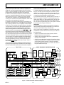 3
3
-
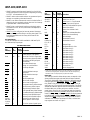 4
4
-
 5
5
-
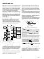 6
6
-
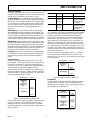 7
7
-
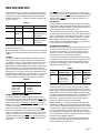 8
8
-
 9
9
-
 10
10
-
 11
11
-
 12
12
-
 13
13
-
 14
14
-
 15
15
-
 16
16
-
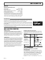 17
17
-
 18
18
-
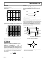 19
19
-
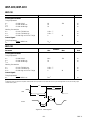 20
20
-
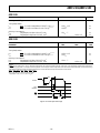 21
21
-
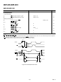 22
22
-
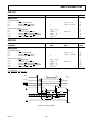 23
23
-
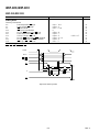 24
24
-
 25
25
-
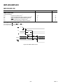 26
26
-
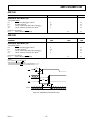 27
27
-
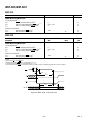 28
28
-
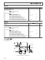 29
29
-
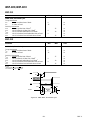 30
30
-
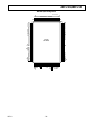 31
31
-
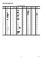 32
32
-
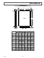 33
33
-
 34
34
-
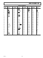 35
35
-
 36
36
-
 37
37
-
 38
38
-
 39
39
-
 40
40


Analog Devices ADSP-2181 User manual
- Category
- Networking
- Type
- User manual
- This manual is also suitable for
Ask a question and I''ll find the answer in the document
Finding information in a document is now easier with AI
Related papers
-
Analog Devices adsp-2100 User manual
-
-
-
-
-
-
-
-
-
Other documents
-
Texas Instruments MSP50C6xx User manual
-
Barco Collaboration Management Suite (CMGS) User guide
-
Freescale Semiconductor 68HC11 Technician Manual
-
Intel 80C186EA User manual
-
 Shenzhen Jiangjing Lighting JHD-TWWR User guide
-
Epson Personal Computer S1C33210 User manual
-
-
Denon DN-S3700 User manual
-
Thule 112181 User manual
-
 Elan Microelectronics EM60000 series User manual

