
ZLE30267 Evaluation Board
PCB Revision B Hardware Guide
December 2015
.

ZLE30267 Hardware Guide Document #153729
December 2015 2
List of Figures ................................................................................................ 3
List of Tables .................................................................................................. 3
Supported Devices ........................................................................................ 5
Related Documents ....................................................................................... 5
Hardware Overview........................................................................................ 5
Hardware Feature Summary ...................................................................................................... 5
Major Components .............................................................................................................. 5
Hardware Features .............................................................................................................. 5
Power Supply ...................................................................................................................... 7
USB Interface ...................................................................................................................... 7
Hardware Configuration ................................................................................ 7
Top Level Configurations ........................................................................................................... 7
Switch and Jumper Configurations, Detailed Listing ......................................................... 12
Connections and Settings Tables ............................................................................................ 14
Power Supply .................................................................................................................... 14
Reset, SPI Bus and GPIO Settings ................................................................................... 16
Local Oscillator .................................................................................................................. 17
DUT Mode Bits .................................................................................................................. 18
Input Clocks ....................................................................................................................... 19
Output Clocks .................................................................................................................... 21
GPIO Header and Status LEDs ............................................................................................... 22
Connecting Off-Board Devices ................................................................................................ 22
Discrete Component Options for Input and Output Clocks ...................................................... 23
Oscillator / Crystal Daughter Card ............................................................. 24
Daughter Card Overview ......................................................................................................... 24
Oscillator Daughter Card Assembly ......................................................................................... 25
Crystal Daughter Card Assembly ............................................................................................. 26
Daughter Card Installation ....................................................................................................... 26
Document Revision History ........................................................................ 28

ZLE30267 Hardware Guide
December 2015 3
List of Figures
Figure 1 · Board Floor Plan ............................................................................................................... 6
Figure 2 · Configuration Topology with Annotations .......................................................................... 8
Figure 3 · Board Configuration 1 ....................................................................................................... 8
Figure 4 · Board Configuration 2 ....................................................................................................... 9
Figure 5 · Board Configuration 3 ....................................................................................................... 9
Figure 6 · Board Configuration 4 ..................................................................................................... 10
Figure 7 · Board Configuration 5 ..................................................................................................... 10
Figure 8 · Board Configurations 6 and 7 ......................................................................................... 11
Figure 9 · Board Configuration 8 ..................................................................................................... 11
Figure 10 · ZLE30267 Oscillator / Crystal Daughter Card Schematic ............................................. 25
Figure 11 · ZLE30267 Oscillator / Crystal Daughter Assembly Drawing ......................................... 25
Figure 12 · ZLE30267 Oscillator / Crystal Daughter Assembly Drawing ......................................... 25
Figure 13 · ZLE30267 Oscillator / Crystal Daughter Assembly Drawing ......................................... 26
Figure 14 · ZLE30267 Oscillator / Crystal Daughter installed on header JP72................................ 27
List of Tables
Table 1 · Serial Bus DIP Switch and Jumper Configurations........................................................... 12
Table 2 · Power Connections and Settings ..................................................................................... 15
Table 3 · Reset, SPI bus and PC Interface Hardware Configuration ............................................... 16
Table 4 · XA Pin Oscillator Configurable Hardware ......................................................................... 17
Table 5 · DUT XA Pin Source Selection Jumper Settings ............................................................... 17
Table 6 · DUT Reset: Mode Bit Settings ......................................................................................... 18
Table 7 · Input Clock Hardware Configuration ................................................................................. 20
Table 8 · Input Clock Differential/Single-Ended Mode Selection Settings ....................................... 20
Table 9 · Output Clock Hardware Configuration .............................................................................. 22
Table 10 · JP1 Serial Header Pin Assignments ............................................................................... 23
Table 11 · JP5 Serial Header Pin Assignments ............................................................................... 23
Table 12 · Discrete Component Options for Clocks ........................................................................ 23

4 December 2015
This page left blank

December 2015 5
ZLE30267 Hardware Guide
Supported Devices
The ZLE30267 evaluation board supports the following Microsemi timing and synchronization devices:
ZL30260 to ZL30267 and ZL40250 to ZL40253.
Related Documents
ZLE30267 Evaluation Board Rev B Schematic
ZLE30267 Evaluation Board Rev B Bill of Materials
Datasheets for the ZL30267 and the other part numbers listed in the Supported Devices section
Hardware Overview
The ZLE30267 Evaluation Board is a test and demonstration platform with support for the full feature sets of
the family of timing ICs.
Hardware Feature Summary
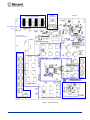
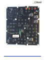
A top side image of the board is shown in Figure 1.
Throughout this document, the abbreviation “DUT” is used to refer to “Device Under Test”, meaning the
Microsemi timing IC on the board.
The ZLE30267 board includes the following major components and hardware features:
Major Components
Timing IC (DUT)
Low noise linear regulators
USB Interface for optional connection to PC with GUI software
External EEPROM for timing device configuration storage (ZL30260, ZL30262, ZL30264, ZL30266,
ZL40250, ZL40252)
SMA connectors for access to all DUT clocks
Serial bus switch
Hardware Features
Single 5VDC external power interface with connector for AC/DC wall adapter
Fully configurable DUT power options
DUT reset switch
Standalone (DIP switch) operation or GUI Interface
USB interface with USB-B connector for PC GUI connection
Pin headers with direct access to board’s SPI/I2C bus. Off-board DUT, EEPROM, or SPI master device
can interface with on-board devices.
Status LEDs
Oscillator options: on board or pluggable TCXOs, XOs or XTALs
SMA connectors on all input and output clocks
Jumper-configurable input clocks
Additional discrete component configuration options for advanced users

ZLE30267 Hardware Guide
6 December 2015
Figure 1 · Board Floor Plan
Power and ground jacks
5V adapter
jack
DUT
USB jack
SPI/I2C
Connectors
Local oscillator selection
LEDs
USB
interface
IC
Reset
button
Device part # and
Info about on-board XOs
VDD
Control
VDD Control
barcode
Output Clocks
Input Clocks

ZLE30267 Hardware Guide
December 2015 7
Power Supply
The board is normally powered via connector J5 using the provided AC-wall-plug 5VDC power supply. Red
LED D1 illuminates to indicate that the board is powered. Advanced power options for lab experimentation
are also provisioned on the board.
USB Interface
The Windows®-based ZLE30267 GUI software communicates with the board via USB connector JDR1.
Hardware Configuration
Top Level Configurations
The ZLE30267 Evaluation Board supports several operational modes of DUTs, including
SPI/I2C slave (with or without internal EEPROM)
SPI master with external EEPROM
To provide flexibility to users, the board supports a multiplicity of configurations, some of which require
software supervision via the USB link, some of which allow the board to operate as a standalone unit, and
others which provide external device access points to the board’s serial bus by means of pin headers.
Top level configuration defines the following aspects of board set up:
A connection between a serial bus master device and serial bus slave device. The serial bus
master may be the USB interface controller (U8), DUT (U17), or an external controller connected
into a pin header (JP1 or JP5) on the board. The serial bus slave device may be the DUT, on-
board EEPROM (U10), or an external EEPROM or DUT on a separate board, connected to a pin
header (JP1 or JP5).
Control of serial bus switch, which may be either via DIP switches or the USB interface controller
Control of DUT GPIO pins by means of DIP switches
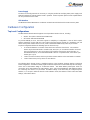
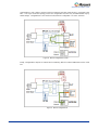
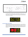
The following block diagram shows a simplified topology of the hardware elements relating to high-level
board configuration. Annotations identify significant board components associated with objects in the image.
At the core of the board’s design is a serial bus switch. The switch allows point-to-point serial bus
connections to be made between the USB interface, DUT, and on board EEPROM, with additional options
for connecting user devices to a pin header. Hardware settings on the board may be configured by DIP
switches, or, in set-ups in which the board is under software control, the software controls some DIP switch
settings, and monitors others.

ZLE30267 Hardware Guide
8 December 2015
Figure 2 · Configuration Topology with Annotations
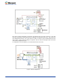
Each of the possible configurations is portrayed in the following series of Figures 3 through 9. The active
serial bus and hardware control elements of the configuration are depicted by heavy lines. Active blocks are
also identified with bold text. Two of the switches on SW1 are shown in green to differentiate them from
GPIO controls. These represent settings for signals IF1 and IF0, which act through the SPI bus and are
used in DUT configuration on reset.
In Configuration 1, the USB interface is SPI master with the DUT as bus slave.
Figure 3 · Board Configuration 1

ZLE30267 Hardware Guide
December 2015 9
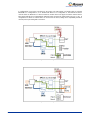
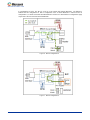
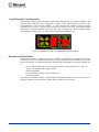
In Configurations 2 and 3, the USB device is SPI master. The USB master can interface with an on-board
EEPROM as in Configuration 2, or an “external SPI device” as in Configuration 3. The external SPI device
could be either an EEPROM or a DUT mounted on another board. The physical form the external device
takes would typically be an independently powered board connected by cable interface to JP1 or JP5. In
configurations in which an external device is connected to the board, voltage level compatibility should be
checked prior to proceeding with connections.
Figure 4 · Board Configuration 2
Figure 5 · Board Configuration 3

ZLE30267 Hardware Guide
10 December 2015
In Configurations 4 and 5, The DUT is set up as a SPI master with external EEPROM. The difference
between the two configurations is that in Configuration 4 the on-board EEPROM is referenced and in
Configuration 5, a header-connected external EEPROM is referenced. Note that these configurations apply
only to DUTs which do not have internal EEPROMs.
Figure 6 · Board Configuration 4
Figure 7 · Board Configuration 5

ZLE30267 Hardware Guide
December 2015 11
Configurations 6 and 7 depict scenarios in which an external serial bus master device is connected to the
DUT. One Figure shows the topology for the two configurations because they are differentiated only by
switch settings. Configuration 6 is SPI serial bus mode, whereas Configuration 7 is an I2C serial bus.
Figure 8 · Board Configurations 6 and 7
Finally, Configuration 8 depicts an external device interfacing with the on-board EEPROM over the serial
bus.
Figure 9 · Board Configuration 8

ZLE30267 Hardware Guide
12 December 2015
Switch and Jumper Configurations, Detailed Listing
Each of the possible board configurations illustrated above is implemented as a collection of settings. The
settings are comprised of jumper assignments, DIP switch settings, and/or software-controlled bit port logic
(1=high, 0=low). This section provides a comprehensive listing of all the board settings for each
configuration. It is important to note that for configurations in which the DUT is an active element, settings
must be applied prior to and held during the DUT reset cycle so that the DUT starts up in a state which is
synchronized with the board.
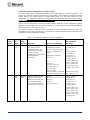
Table 1 lists the configurations and their associated settings. References to the configuration topology
diagrams in the preceding section are shown in column 1. A summary listing of the Jumpers and switches
referenced in Table 1 can be found in Table 3.
The reader is referred to applicable device datasheets for further information about DUT reset and
configuration. Some signals, typically GPIOs, may change once DUT has initialized. Note: at this time not all
configurations are fully supported by software.
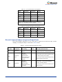
Table 1 · Serial Bus DIP Switch and Jumper Configurations
Board
Config.
Number
Serial
Bus
Master
Serial
Bus Slave
Description
Switch and Jumper Settings
USB Controller IO
Pin Settings
1
USB
(SPI)
DUT
GUI/PC is master of SPI bus,
and controls serial bus
configuration settings. DIP
switch settings control DUT
GPIOs. DUT loads
configuration from internal ROM
or EEPROM (device-
dependent).
JP9 = on
ZL30260/2/4/6, ZL40250/2:
SW1.IF0 = 0 (ROM auto-config)
SW1.IF0 = 1 (EEPROM auto-
config)
ZL30261/3/5/7, ZL40251/3:
SW1.IF0 = 1
Plus:
SW1.IF1 = 1
SW1.TEST_GPIO3 = 0
SW1.PUPD_ENB = 0
[SW1.AC2_GPIO2,
SW1.AC1_GPIO1,
SW1.AC0_GPIO0] = select ROM
or EEPROM configuration # 0 to 7
On RESET,
FT_DSW_SEL = 1;
plus:
FT_FSW_OEB = 0
FT_HW_SEL = 0
FT_SPI_SEL = 0
FT_ESW_SEL = 1
FT_ESW_OEB = 0
FT_PUPD_ENB = hi-Z
FT_AC0_GPIO0 = hi-Z
FT_AC1_GPIO1 = hi-Z
FT_AC2_GPIO2 = hi-Z
FT_TEST_GPIO3 = hi-Z
After DUT auto-config,
set FT_DSW_SEL = 0
2
USB
(SPI)
EEPROM
(U10)
GUI/PC Is master of SPI bus
connection with on-board
EEPROM, and controls serial
bus configuration settings
If DUT is running, GPIO DIPs
should be left as configured.
JP9=on
JP6: shunt pins 1-2, 3-4, 5-6, 7-8
SW1.IF0 = 1
SW1.IF1 = 1
SW1.PUPD_ENB = 0
FT_FSW_OEB = 0
FT_HW_SEL = 0
FT_SPI_SEL = 1
FT_DSW_SEL = x
FT_ESW_SEL = 0
FT_ESW_OEB = 0
FT_PUPD_ENB = hi-Z
FT_AC0_GPIO0 = hi-Z
FT_AC1_GPIO1 = hi-Z
FT_AC2_GPIO2 = hi-Z
FT_TEST_GPIO3 = hi-Z
FT_GPIO3 = hi-Z

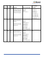
ZLE30267 Hardware Guide
December 2015 13
Board
Config.
Number
Serial
Bus
Master
Serial
Bus Slave
Description
Switch and Jumper Settings
USB Controller IO
Pin Settings
3
USB
(SPI)
JP1 or
JP5
GUI/PC controls external
EEPROM connected at header,
or external DUT via SPI cable,
and serial bus configuration.
If DUT is running, GPIO DIPs
should be left as configured.
JP9 = on
JP6: all open
SW1.IF0 = 1
SW1.IF1 = 1
SW1.PUPD_ENB = 0
FT_FSW_OEB = 0
FT_HW_SEL = 0
FT_SPI_SEL = 1
FT_DSW_SEL = x
FT_ESW_SEL = 0
FT_ESW_OEB = 0
FT_PUPD_ENB = hi-Z
FT_AC0_GPIO0 = hi-Z
FT_AC1_GPIO1 = hi-Z
FT_AC2_GPIO2 = hi-Z
FT_TEST_GPIO3 = hi-Z
FT_GPIO3 = hi-Z
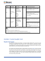
4
DUT
(SPI)
EEPROM
ZL30260/2/4/6 and ZL40250/2
DUT loads from on-board
EEPROM (standalone board
operation).
ZL30261/3/5/7 and ZL40251/3
DUT will not load from external
EEPROM device.
JP9 = open
JP6: shunt pins 1-2, 3-4, 5-6, 7-8
SW1.IF0 = 1
SW1.IF1 = 1
SW1.TEST_GPIO3 = 0
SW1.PUPD_ENB = 0
SW2.DSW_SEL = 1
SW2. ESW_OEB = 0
SW2. ESW_SEL = 1
[SW1.AC2_GPIO2,
SW1.AC1_GPIO1,
SW1.AC0_GPIO0] = select
EEPROM configuration # 0 to 7
N/A
5
DUT
(SPI)
JP1 or
JP5
Header
ZL30260/2/4/6 and ZL40250/2
DUT loads from external
EEPROM connected to header.
ZL30261/3/5/7 and ZL40251/3
DUT will not load from external
EEPROM device.
JP9 = open
JP6: open
SW1.IF0 = 1
SW1.IF1 = 1
SW1.TEST_GPIO3 = 0
SW1.PUPD_ENB = 0
SW2.DSW_SEL = 1
SW2. ESW_OEB = 0
SW2.ESW_SEL = 1
SW1.AC2_GPIO2,
SW1.AC1_GPIO1,
SW1.AC0_GPIO0 = select
EEPROM configuration # 0 to 7
N/A

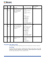
ZLE30267 Hardware Guide
14 December 2015
Board
Config.
Number
Serial
Bus
Master
Serial
Bus Slave
Description
Switch and Jumper Settings
USB Controller IO
Pin Settings
6
JP1 or
JP5
Header
DUT
External connected device as
SPI master, local DUT as SPI
slave. External EEPROMs
cannot be used with this
configuration.
JP9 = open
JP6: open
ZL30260/2/4/6, ZL40250/2:
SW1.IF0 = 0
ZL30261/3/5/7, ZL40251/3:
SW1.IF0 = 1
Plus:
SW1.IF1 = 1
SW1.TEST_GPIO3 = 0
SW1.PUPD_ENB = 0
SW2.DSW_SEL = 1
SW2. ESW_OEB = 0
SW2. ESW_SEL = 1
SW1.AC2_GPIO2,
SW1.AC1_GPIO1,
SW1.AC0_GPIO0 = select ROM/
EEPROM configuration # 0 to 7
N/A
7
JP1 or
JP5
Header
DUT
External connected device as
I2C master, local DUT as I2C
slave. External EEPROMs
cannot be used with this
configuration.
JP9 = open
JP6: open
SW1.IF1, SW1.IF0 = I2C device
address – see datasheet
SW1.TEST_GPIO3 = 0
SW1.PUPD_ENB = 0
SW2.DSW_SEL = 1
SW2. ESW_OEB = 0
SW2. ESW_SEL = 1
SW1.AC2_GPIO2,
SW1.AC1_GPIO1,
SW1.AC0_GPIO0 = select ROM/
EEPROM configuration # 0 to 7
N/A
8
JP1 or
JP5
Header
EEPROM
External device SPI master
programs and/or reads
EEPROM
JP9 = open
JP6: shunt pins 1-2, 3-4, 5-6, 7-8
SW1.IF0 = 1
SW1.IF1 = 1
SW1.PUPD_ENB = 0
SW2. ESW_OEB = 1
N/A
Connections and Settings Tables
The following sections provide detailed listings of the various evaluation board user interface components.
Power Supply
The board provides several options for evaluating device performance with respect to power supply
configuration. DUT power configuration is highly customizable. A thorough understanding of the DUT and
board operation should be developed prior to customizing power settings on the board. Table 2 summarizes
the power supply related hardware connectors and their functions.

ZLE30267 Hardware Guide
December 2015 15
Table 2 · Power Connections and Settings
Silkscreen
Reference
Device/
Function
Basic Setting
Schematic
Sheet
Description
J1/BJ1
Power jack
Unconnected
4
Optional 5V Power interface
J2/BJ2 (GND)
Banana jack
Unconnected
4
Optional power interface GND
J5 (5V)
Power jack
Connect to 5V
4
5V Power adapter (2.1 mm x 5.5 mm barrel jack)
J3/BJ3 (PWR AUX1)
Banana jack
Unconnected
4
Direct DUT power interface AUX1
J4/BJ4 (PWR AUX2)
Banana jack
Unconnected
4
Direct DUT power option AUX2
J6 (PWR IN/OUT)
SMA
Unconnected
4
Power noise inject/monitor site to AUX1
J7 (PWR IN/OUT)
SMA
Unconnected
4
Power noise inject/monitor site to AUX2
JP32
6 pin header
Shunt pins 1-3
5
Selects VDDH_P DUT voltage source (3.3V LDO, 2.5V LDO,
AUX1, AUX2)
JP46
6 pin header
Shunt pins 1-3
5
Selects VSELH voltage (same as VDDH_P, 2.5V LDO, AUX1,
AUX2)
JP26
10 pin header
Shunt pins 1-3
5
Selects VDDL_1 DUT voltage source (VSELH, 2.5V LDO, 1.8V
LDO, AUX1, AUX2)
JP21
10 pin header
Shunt pins 1-3
5
Selects VDDIO DUT voltage source (VSELH, 2.5V LDO, 1.8V
LDO, AUX1, AUX2)
JP71
10 pin header
Shunt pins 1-3
5
Selects VDDOA DUT voltage source (VSELH, 2.5V LDO, 1.8V
LDO, 1.5V LDO, AUX1, AUX2)
JP68
10 pin header
Shunt pins 1-3
5
Selects VDDOB DUT voltage source (VSELH, 2.5V LDO, 1.8V
LDO, 1.5V LDO, AUX1, AUX2)
JP65
10 pin header
Shunt pins 1-3
5
Selects VDDOC DUT voltage source (VSELH, 2.5V LDO, 1.8V
LDO, 1.5V LDO, AUX1, AUX2)
JP59
10 pin header
Shunt pins 1-3
5
Selects VDDOD DUT voltage source (VSELH, 2.5V LDO, 1.8V
LDO, 1.5V LDO, AUX1, AUX2)
JP41
10 pin header
Shunt pins 1-3
5
Selects VDDOE DUT voltage source (VSELH, 2.5V LDO, 1.8V
LDO, 1.5V LDO, AUX1, AUX2)
JP19
10 pin header
Shunt pins 1-2
5
Selects VDDOF DUT voltage source (VSELH, 2.5V LDO, 1.8V
LDO, 1.5V LDO, AUX1, AUX2)
JP49
3-pin header
Not installed
5
Probe/configuration option for VDDH_P power pin
JP63
3-pin header
Not installed
5
Probe/configuration option for VDDH_1 power pin
JP15
3-pin header
Not installed
5
Probe/configuration option for VDDH_2 power pin
JP18
3-pin header
Not installed
5
Probe/configuration option for VDDL_1 power pin
JP62
3-pin header
Not installed
5
Probe/configuration option for VDDL_2 power pin
JP16
3-pin header
Not installed
5
Probe/configuration option for VDDL_3 power pin
JP17
3-pin header
Not installed
5
Probe/configuration option for VDDIO power pin
JP61
3-pin header
Not installed
5
Probe/configuration option for VDDOA power pin
JP60
3-pin header
Not installed
5
Probe/configuration option for VDDOB power pin
JP53
3-pin header
Not installed
5
Probe/configuration option for VDDOC power pin
JP27
3-pin header
Not installed
5
Probe/configuration option for VDDOD power pin

ZLE30267 Hardware Guide
16 December 2015
Silkscreen
Reference
Device/
Function
Basic Setting
Schematic
Sheet
Description
JP22
3-pin header
Not installed
5
Probe/configuration option for VDDOE power pin
JP14
3-pin header
Not installed
5
Probe/configuration option for VDDOF power pin
JP70 (VOSC)
3 pin header
Shunt pins 1-2
4
Sets oscillator voltage (shunt pins 1-2=3.3V, shunt pins 2-3=
2.5V, open = 1.8V)
Reset, SPI Bus and GPIO Settings
The board has a number of DUT variants and configurations, some of which support GUI/PC software and
some of which are standalone operation. Table 3 lists the hardware interfaces which are related to SPI bus,
resets, and DUT configuration. This table provides a physical description and summary of the configurable
hardware components referenced in Table 1.
Table 3 · Reset, SPI bus and PC Interface Hardware Configuration
Silkscreen
Reference
Device/ Function
Basic Setting
Schematic
Sheet
Description
JDR1 (USB)
USB connector
Connected to PC
2
Connects board to host computer
JP9 (PWREN#)
2 pin header
Shunt installed
2
Enables USB interface controls on board
JP2
2 pin header
Shunt installed
2
Serial bus voltage translator reference voltage
S2 (DUT
RESET)
Reset pushbutton
Inactive
2
Sends a reset signal to DUT.
JP1
10 pin header
Unconnected
3
Can be used to connect an external SPI or I2C master to
DUT or EEPROM on board
JP6
8 pin header
Shunts on pins 1-2,
3-4, 5-6, 7-8
3
Connects EEPROM to switched SPI bus
JP3
3 pin header
Shunt on pins 1-2
3
Configure JP1 as SPI SCLK or I2C SCL
JP4
3 pin header
Shunt on pins 1-2
3
Configure JP1 as SPI SI or I2C SDA
JP5
8 pin header
No shunts
3
Probe/test serial header for EEPROM or DUT
JP7
10 pin header
No shunts
3
Test/ pull down header for DUT GPIO pins
SW2
4 DIP switch
Depends on
Configuration
3
SPI bus switch hardware configuration (may be overdriven
by USB controller)
SW1
8 DIP switch
Depends on
Configuration
3
DUT hardware configuration pin and GPIO hardware
configuration switches. GPIO switches may be overdriven
by USB controller (not currently supported by GUI)
TP35, TP36,
TP38, TP40
Testpoints
N/A
3
Test points for probing SPI bus at DUT
J15
SMA Connector
3
DUT AC0_GPIO0 connection point
JP12
2 pin header
Shunt installed
3
Connect DUT AC0_GPIO0 to LEDs/local controller port
J16
SMA Connector
3
DUT AC1_GPIO1 connection point
JP13
2 pin header
Shunt installed
3
Connect DUT AC1_GPIO1 to LEDs/local controller port
J11
SMA Connector
3
DUT AC2_GPIO2 connection point
JP11
2 pin header
Shunt installed
3
Connect DUT AC2_GPIO2 to LEDs/local controller port

ZLE30267 Hardware Guide
December 2015 17
Silkscreen
Reference
Device/ Function
Basic Setting
Schematic
Sheet
Description
J20
SMA Connector
3
DUT TEST_GPIO3 connection point
JP20
2 pin header
Shunt installed
3
Connect DUT TEST_GPIO3 to LEDs/local controller port
Local Oscillator
The board provides several options for driving the timing device’s XA input pin from an on-board oscillator,
crystal, or an external source. Table 4 summarizes the oscillator related hardware jumpers and connectors
and functionality. Table 5 summarizes board jumper settings required to set up each clock source.
Table 4 · XA Pin Oscillator Configurable Hardware
Silkscreen
Reference
Device/ Function
Basic Setting
Schematic
Sheet
Description
JP69
6 pin header
Shunt pins 5-6
7
2-pin shunt installed connects OSC power (see JP70) to one
of three oscillators (pins 1-2= JP67 header for daughter card;
pins 3-4 = Y2; pins 5-6= Y3)
JP67
10-pin receptacle for
oscillator daughter
board
7
Microsemi custom daughter board installs here.
JP64
10 pin header
Shunt pins 1-3
7
XA pin clock patch header. Shunt settings are as follows:
pins 1-2: JP67 to J31 (monitor JP67)
pins 1-3: JP67 to DUT XA pin
pins 3-5: Y2 to DUT XA pin
pins 5-7: Y2 to J31 (monitor Y2)
pins 4-6: Y3 to DUT XA pin
pins 6-8: Y3 toJ31 (monitor Y3)
pins 2-4: J31 to DUT XA pin (external clock in)
J31
SMA connector
7
Access point for monitoring an oscillator on board, or providing
DUT XA pin clock from an external clock source
JP66
2 pin header
Open
7
Open selects AC coupled clock connection to J31; shunt
selects DC coupling to J31
JP72
6 pin header
Shunt pins 3-4
7
Header for mounting optional XTAL or oscillator device.
Located on bottom side of board. Shunt on pins 3-4 patches
oscillator signal from patch header JP64 to DUT XA pin
Table 5 · DUT XA Pin Source Selection Jumper Settings
Clock Source
Jumper Settings
Y2 on-board 3.2mm x 2.5mm single-ended oscillator site
JP69 = shunt pin 3-4
JP64 = shunt pin 3-5
JP72 = shunt pin 3-4
JP70 = Osc voltage. Open=1.8V; shunt pins 1-2 =3.3V; shunt pins
2-3= 2.5V

ZLE30267 Hardware Guide
18 December 2015
Clock Source
Jumper Settings
Y3 on-board 5mm x7mm single-ended oscillator site
JP69 = shunt pin 5-6
JP64 = shunt pin 4-6
JP72 = shunt pin 3-4
JP70 = Osc voltage. Open=1.8V; shunt pins 1-2 =3.3V; shunt pins
2-3= 2.5V
JP67 oscillator daughter card
JP67 = 10-pin custom oscillator daughter board
JP69 = shunt pin 1-2
JP64 = shunt pin 1-3
JP72 = shunt pin 3-4
JP70 = Osc voltage. Open=1.8V; shunt pins 1-2 =3.3V; shunt pins
2-3= 2.5V
J31 external single-ended Input
JP69 = open
JP64 = shunt pin 2-4
JP72 = shunt pin 3-4
JP66 = shunt for DC coupled; open for AC coupled
JP70 = n/a
JP72 external daughter card xtal/osc site
JP69 = open
JP72 = install custom daughter card
JP70 = Osc voltage. Open=1.8V; shunt pins 1-2 =3.3V; shunt pins
2-3= 2.5V
DUT Mode Bits
The various combinations of GPIO[2,1,0] and IF[1,0] mode bits which apply during DUT reset are
summarized in Table 6. As described in the timing device datasheets, these five bits determine the operating
mode of the DUT with respect to its serial bus interface and configuration data fill selection. Serial bus
steering must be coordinated with mode bits as described in Table1.
Table 6 · DUT Reset: Mode Bit Settings
DUT Type
DUT Mode
Settings (DIP controlled)
Settings (GUI Controlled, on reset)
Internal ROM,
optional external
EEPROM
SPI slave,
Load ROM
configuration
SW1.IF0 = 0
SW1.IF1 = 1
ROM configuration select= [SW1.AC2_GPIO2,
SW1.AC1_GPIO1, SW1.AC0_GPIO0]
FT_CSN= 1 or HiZ
FT_SO = 1 or HiZ
FT_AC2_GPIO2 = HiZ
FT_AC1_GPIO1 = HiZ
FT_AC0_GPIO0 = HiZ
Internal ROM,
optional external
EEPROM
SPI slave,
Load external
EEPROM
SW1.IF0 = 1
SW1.IF1 = 1
EEPROM configuration select=
[SW1.AC2_GPIO2, SW1.AC1_GPIO1,
SW1.AC0_GPIO0]
FT_CSN= 1 or HiZ
FT_SO = 1 or HiZ
FT_AC2_GPIO2 = HiZ
FT_AC1_GPIO1 = HiZ
FT_AC0_GPIO0 = HiZ
Internal EEPROM
SPI slave,
Load internal
EEPROM
configuration
SW1.IF0 = 1
SW1.IF1 = 1
EEPROM configuration select=
[SW1.AC2_GPIO2, SW1.AC1_GPIO1,
SW1.AC0_GPIO0]
FT_CSN= 1 or HiZ
FT_SO = 1 or HiZ
FT_AC2_GPIO2 = HiZ
FT_AC1_GPIO1 = HiZ
FT_AC0_GPIO0 = HiZ
Internal ROM
I2C Slave
I2C address: [SW1.IF1,SW1.IF0 ] = [0,0] or
[0,1]
EEPROM configuration select=
[SW1.AC2_GPIO2, SW1.AC1_GPIO1,
SW1.AC0_GPIO0]
N/A, not supported by GUI

ZLE30267 Hardware Guide
December 2015 19
DUT Type
DUT Mode
Settings (DIP controlled)
Settings (GUI Controlled, on reset)
Internal EEPROM
I2C Slave
I2C address: [SW1.IF1,SW1.IF0 ] = [0,0] or
[0,1] or [1,0]
EEPROM configuration select=
[SW1.AC2_GPIO2, SW1.AC1_GPIO1,
SW1.AC0_GPIO0]
N/A, not supported by GUI
Notes
For all DUT modes, TEST_GPIO3 = 0 whether by DIP control or GUI control.
See Table 1 for further details on configuration modes.
Input Clocks
The board’s IC1 and IC2 clock inputs can be configured to accept either a differential or single-ended signal
using jumpers. When configured as a differential input, IC1 or IC2 can be configured as either AC-coupled
or DC-coupled. IC3 is a single-ended input by definition, and can be configured to be either AC-coupled or
DC-coupled. Table 7 summarizes the input clock related hardware connectors and functionality. Table 8
shows how to configure the ICx jumpers for either a differential or single-ended input.

ZLE30267 Hardware Guide
20 December 2015
Table 7 · Input Clock Hardware Configuration
Silkscreen
Reference
Device/ Function
Basic Setting
Schematic
Sheet
Description
J27 (IC1P)
J28 (IC1N)
SMA connectors
Differential clock input
7
IC1 differential or single-ended input. Various
configurations are created using JP54, JP55,
JP44, JP45
JP54, JP55
3-pin headers
Shunt pins 2-3
7
JP54 applies to IC1P. JP55 applies to IC1N.
Settings:
Open = AC coupled input
Shunt pins 1-2 = AC-couple DUT pin to GND
(unused)
Shunt pins 2-3 = DC-coupled signal
JP44, JP45
JP44: shunt (default) terminates IC1P/N as 100
ohms differential. Remove for single ended
operation.
JP45: normally open. Shunt to terminate IC1P as
50 ohms to GND (and optionally IC1N if JP44 is
installed)
J24 (IC2P)
J23 (IC2N)
SMA connectors
Differential clock input
7
IC2 differential or single-ended input. Various
configurations are created using JP36, JP35,
JP39, JP40
JP36, JP35
3-pin headers
Open
7
JP36 applies to IC2P. JP35 applies to IC2N.
Settings:
Open = AC coupled input
Shunt pins 1-2 = AC-couple DUT pin to GND
(unused)
Shunt pins 2-3 = DC-coupled signal
JP39, JP40
2-pin headers
Shunt JP30
7
JP39: shunt (default) terminates IC2P/N as 100
ohms differential. Remove for single ended
operation.
JP40: normally open. Shunt to terminate IC2P as
50 ohms to GND (and optionally IC2N if JP39 is
installed)
J19 (IC3)
SMA connector
AC coupled clock input
7
Single ended clock input with configuration
options
JP31
2-pin header
Shunt pins 1-2
7
Header open connects DUT IC3 pin to J31 SMA
jack as AC coupled
Shunt connects DUT IC3 pin to J31 SMA as DC
coupled
Table 8 · Input Clock Differential/Single-Ended Mode Selection Settings
Input Clock
Mode
Coupling
Jumper Settings
IC1
Differential
AC (100 ohms
differential load)
JP54 = open
JP55 = open
JP45 = open
JP44 = installed
Page is loading ...
Page is loading ...
Page is loading ...
Page is loading ...
Page is loading ...
Page is loading ...
Page is loading ...
Page is loading ...
Page is loading ...
Page is loading ...
-
 1
1
-
 2
2
-
 3
3
-
 4
4
-
 5
5
-
 6
6
-
 7
7
-
 8
8
-
 9
9
-
 10
10
-
 11
11
-
 12
12
-
 13
13
-
 14
14
-
 15
15
-
 16
16
-
 17
17
-
 18
18
-
 19
19
-
 20
20
-
 21
21
-
 22
22
-
 23
23
-
 24
24
-
 25
25
-
 26
26
-
 27
27
-
 28
28
-
 29
29
-
 30
30


Ask a question and I''ll find the answer in the document
Finding information in a document is now easier with AI
Related papers
-
Microsemi LX8204 12 V E-Fuse User manual
-
-
-
-
-
Microsemi SmartFusion2 User manual
-
-
-
-
Other documents
-
Texas Instruments LMK03318EVM User guide
-
-
-
Xilinx ZCU1285 User manual
-
NXP BSC9132QDS Reference guide
-
NXP P5010 User manual
-
Microchip Technology BM70 PICtail User manual
-
-
Silicon Labs Si5386A-E Evaluation Board User guide
-
Analog Devices ADuCM4050 EZ-KIT User manual