Page is loading ...

SmartFusion Development Kit
User’s Guide

SmartFusion Development Kit
Revision 7 2
Table of Contents
Introduction . . . . . . . . . . . . . . . . . . . . . . . . . . . . . . . . . . . . . . . . . . . . . . . . . . . . . . . . . . . . . . . . . . . . . . 5
Kit Contents . . . . . . . . . . . . . . . . . . . . . . . . . . . . . . . . . . . . . . . . . . . . . . . . . . . . . . . . . . . . . . . . . . . . . . . . . . . . . . . 6
SmartFusion Development Kit Web Resources . . . . . . . . . . . . . . . . . . . . . . . . . . . . . . . . . . . . . . . . . . . . . . . . . . . . 6
Board Description . . . . . . . . . . . . . . . . . . . . . . . . . . . . . . . . . . . . . . . . . . . . . . . . . . . . . . . . . . . . . . . . . . . . . . . . . . 6
1 Installation and Settings. . . . . . . . . . . . . . . . . . . . . . . . . . . . . . . . . . . . . . . . . . . . . . . . . . . . . . . . . . . . . 9
Software Installation . . . . . . . . . . . . . . . . . . . . . . . . . . . . . . . . . . . . . . . . . . . . . . . . . . . . . . . . . . . . . . . . . . . . . . . . . 9
Hardware Installation . . . . . . . . . . . . . . . . . . . . . . . . . . . . . . . . . . . . . . . . . . . . . . . . . . . . . . . . . . . . . . . . . . . . . . . . 9
2 Hardware Components . . . . . . . . . . . . . . . . . . . . . . . . . . . . . . . . . . . . . . . . . . . . . . . . . . . . . . . . . . . . 15
SmartFusion cSoC Description and Connections . . . . . . . . . . . . . . . . . . . . . . . . . . . . . . . . . . . . . . . . . . . . . . . . . 15
I/O Pin Connections . . . . . . . . . . . . . . . . . . . . . . . . . . . . . . . . . . . . . . . . . . . . . . . . . . . . . . . . . . . . . . . . . . . . . . . . 16
SmartFusion cSoC Hard ARM Cortex-M3 Processor . . . . . . . . . . . . . . . . . . . . . . . . . . . . . . . . . . . . . . . . . . . . . . 17
Power Sources . . . . . . . . . . . . . . . . . . . . . . . . . . . . . . . . . . . . . . . . . . . . . . . . . . . . . . . . . . . . . . . . . . . . . . . . . . . . 18
3 Components Description and Operation . . . . . . . . . . . . . . . . . . . . . . . . . . . . . . . . . . . . . . . . . . . . . . . 19
VAREF Connections . . . . . . . . . . . . . . . . . . . . . . . . . . . . . . . . . . . . . . . . . . . . . . . . . . . . . . . . . . . . . . . . . . . . . . . 19
Current Sensing Circuit . . . . . . . . . . . . . . . . . . . . . . . . . . . . . . . . . . . . . . . . . . . . . . . . . . . . . . . . . . . . . . . . . . . . . 20
PWM Circuit . . . . . . . . . . . . . . . . . . . . . . . . . . . . . . . . . . . . . . . . . . . . . . . . . . . . . . . . . . . . . . . . . . . . . . . . . . . . . . 20
Push-Button System Reset . . . . . . . . . . . . . . . . . . . . . . . . . . . . . . . . . . . . . . . . . . . . . . . . . . . . . . . . . . . . . . . . . . 21
Push-Button, DIP Switches, and User LEDs . . . . . . . . . . . . . . . . . . . . . . . . . . . . . . . . . . . . . . . . . . . . . . . . . . . . . 22
One-Bit DAC (OBD) Circuit . . . . . . . . . . . . . . . . . . . . . . . . . . . . . . . . . . . . . . . . . . . . . . . . . . . . . . . . . . . . . . . . . . 24
OLED Display . . . . . . . . . . . . . . . . . . . . . . . . . . . . . . . . . . . . . . . . . . . . . . . . . . . . . . . . . . . . . . . . . . . . . . . . . . . . 25
SPI Flash . . . . . . . . . . . . . . . . . . . . . . . . . . . . . . . . . . . . . . . . . . . . . . . . . . . . . . . . . . . . . . . . . . . . . . . . . . . . . . . . 28
SPI DAC . . . . . . . . . . . . . . . . . . . . . . . . . . . . . . . . . . . . . . . . . . . . . . . . . . . . . . . . . . . . . . . . . . . . . . . . . . . . . . . . . 29
I
2
C EEPROM . . . . . . . . . . . . . . . . . . . . . . . . . . . . . . . . . . . . . . . . . . . . . . . . . . . . . . . . . . . . . . . . . . . . . . . . . . . . . 30
Clock Oscillator . . . . . . . . . . . . . . . . . . . . . . . . . . . . . . . . . . . . . . . . . . . . . . . . . . . . . . . . . . . . . . . . . . . . . . . . . . . 32
USB-to-UART Interface . . . . . . . . . . . . . . . . . . . . . . . . . . . . . . . . . . . . . . . . . . . . . . . . . . . . . . . . . . . . . . . . . . . . . 33
RS485 Interface . . . . . . . . . . . . . . . . . . . . . . . . . . . . . . . . . . . . . . . . . . . . . . . . . . . . . . . . . . . . . . . . . . . . . . . . . . . 34
Ethernet Interface . . . . . . . . . . . . . . . . . . . . . . . . . . . . . . . . . . . . . . . . . . . . . . . . . . . . . . . . . . . . . . . . . . . . . . . . . 35
Memory Section Overview . . . . . . . . . . . . . . . . . . . . . . . . . . . . . . . . . . . . . . . . . . . . . . . . . . . . . . . . . . . . . . . . . . . 37
Using EMC I/Os as User I/Os . . . . . . . . . . . . . . . . . . . . . . . . . . . . . . . . . . . . . . . . . . . . . . . . . . . . . . . . . . . . . . . . 45
Controller Area Network (CAN) Interface . . . . . . . . . . . . . . . . . . . . . . . . . . . . . . . . . . . . . . . . . . . . . . . . . . . . . . . . 45
Ethernet for Control Automation Technology (EtherCAT) Interface . . . . . . . . . . . . . . . . . . . . . . . . . . . . . . . . . . . . 46
Low Cost Programming Stick (LCPS) Header . . . . . . . . . . . . . . . . . . . . . . . . . . . . . . . . . . . . . . . . . . . . . . . . . . . . 47
RealView Header . . . . . . . . . . . . . . . . . . . . . . . . . . . . . . . . . . . . . . . . . . . . . . . . . . . . . . . . . . . . . . . . . . . . . . . . . . 48
Direct-C Programming Interface . . . . . . . . . . . . . . . . . . . . . . . . . . . . . . . . . . . . . . . . . . . . . . . . . . . . . . . . . . . . . . 49
FlashPro4 Programming Header . . . . . . . . . . . . . . . . . . . . . . . . . . . . . . . . . . . . . . . . . . . . . . . . . . . . . . . . . . . . . . 50
A2F500 Digital I/O Expansion Header . . . . . . . . . . . . . . . . . . . . . . . . . . . . . . . . . . . . . . . . . . . . . . . . . . . . . . . . . . 54
Mixed Signal Header . . . . . . . . . . . . . . . . . . . . . . . . . . . . . . . . . . . . . . . . . . . . . . . . . . . . . . . . . . . . . . . . . . . . . . . 56
4 Pin List . . . . . . . . . . . . . . . . . . . . . . . . . . . . . . . . . . . . . . . . . . . . . . . . . . . . . . . . . . . . . . . . . . . . . . . . . 61
Pin List for A2F500M3G-FGG484ES Devices . . . . . . . . . . . . . . . . . . . . . . . . . . . . . . . . . . . . . . . . . . . . . . . . . . . . 61
5 Board Stackup . . . . . . . . . . . . . . . . . . . . . . . . . . . . . . . . . . . . . . . . . . . . . . . . . . . . . . . . . . . . . . . . . . . 75

Table of Contents
3 Revision 7
A2F500-DEV-KIT-2 Board Stack-Up . . . . . . . . . . . . . . . . . . . . . . . . . . . . . . . . . . . . . . . . . . . . . . . . . . . . . . . . . . . 75
6 Manufacturing Test. . . . . . . . . . . . . . . . . . . . . . . . . . . . . . . . . . . . . . . . . . . . . . . . . . . . . . . . . . . . . . . . 79
A2F500-DEV-KIT-2 Board Testing Procedures . . . . . . . . . . . . . . . . . . . . . . . . . . . . . . . . . . . . . . . . . . . . . . . . . . . 79
Jumper Settings for the Board Test . . . . . . . . . . . . . . . . . . . . . . . . . . . . . . . . . . . . . . . . . . . . . . . . . . . . . . . . . . . . 79
Installing the A2F500-DEV-KIT-2 Board USB Serial Driver . . . . . . . . . . . . . . . . . . . . . . . . . . . . . . . . . . . . . . . . . . 80
Hooking up the Board and Programming Stick . . . . . . . . . . . . . . . . . . . . . . . . . . . . . . . . . . . . . . . . . . . . . . . . . . . 80
Programming the A2F500-DEV-KIT-2 Board (SmartFusion cSoC Device) . . . . . . . . . . . . . . . . . . . . . . . . . . . . . . 82
Setting Up the Test Terminal . . . . . . . . . . . . . . . . . . . . . . . . . . . . . . . . . . . . . . . . . . . . . . . . . . . . . . . . . . . . . . . . . 85
Running the A2F500-DEV-KIT-2 Board Test . . . . . . . . . . . . . . . . . . . . . . . . . . . . . . . . . . . . . . . . . . . . . . . . . . . . . 89
A2F500-DEV-KIT-2 Board Failures . . . . . . . . . . . . . . . . . . . . . . . . . . . . . . . . . . . . . . . . . . . . . . . . . . . . . . . . . . . 112
A List of Changes . . . . . . . . . . . . . . . . . . . . . . . . . . . . . . . . . . . . . . . . . . . . . . . . . . . . . . . . . . . . . . . . . 113
B Product Support . . . . . . . . . . . . . . . . . . . . . . . . . . . . . . . . . . . . . . . . . . . . . . . . . . . . . . . . . . . . . . . . . 115
Customer Service . . . . . . . . . . . . . . . . . . . . . . . . . . . . . . . . . . . . . . . . . . . . . . . . . . . . . . . . . . . . . . . . . . . . . . . . 115
Customer Technical Support Center . . . . . . . . . . . . . . . . . . . . . . . . . . . . . . . . . . . . . . . . . . . . . . . . . . . . . . . . . . 115
Technical Support . . . . . . . . . . . . . . . . . . . . . . . . . . . . . . . . . . . . . . . . . . . . . . . . . . . . . . . . . . . . . . . . . . . . . . . . 115
Website . . . . . . . . . . . . . . . . . . . . . . . . . . . . . . . . . . . . . . . . . . . . . . . . . . . . . . . . . . . . . . . . . . . . . . . . . . . . . . . . 115
Contacting the Customer Technical Support Center . . . . . . . . . . . . . . . . . . . . . . . . . . . . . . . . . . . . . . . . . . . . . . 115
ITAR Technical Support . . . . . . . . . . . . . . . . . . . . . . . . . . . . . . . . . . . . . . . . . . . . . . . . . . . . . . . . . . . . . . . . . . . . 116
Index . . . . . . . . . . . . . . . . . . . . . . . . . . . . . . . . . . . . . . . . . . . . . . . . . . . . . . . . . . . . . . . . . . . . . . . . . 117


Revision 7 5
Introduction
The RoHS-compliant SmartFusion
®
Development Kit (A2F500-DEV-KIT-2) enables designers to develop
applications that involve one or more of the following:
• Microcontroller applications
• Real-time operating system (RTOS)/OS development
• Embedded ARM
®
Cortex™-M3 processor based systems
• Motor control
• System management
• Power sequencing, trimming, and management
• Touch screen display control
• Audio processing
•FieldBus
®
demonstrator
•EtherCAT
®
• Industrial network
The board also provides a standard 100-pin mixed signal header for interfacing to the analog pins. This
provides access for plugging in a daughter board with a mixed signal interface.
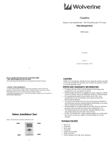
Figure 1 • A2F500-DEV-KIT-2
DirectC Header
Board Reset Switch
Power Jack
Memory Device
Configuration Headers
AGLP DIP Switch
AGLP125V5-
CSG289
IGLOO PLUS Header
10/100 Ethernet PHY
RJ45 Connector for
10/100 Ethernet
AGLP Header
DACOUT/
ADC Headers
RJ45 Connectors for
EtherCAT Ports
SmartFusion Device
DB9 Connector
for CAN0
SRAM
(3.3 V)
CAN
Transceivers
DB9 Connector
for CAN1
A2F500
Connector
PSRAM
(1.8 V)
LCPS Connector
FlashPro Header
DIP Switch
JTAG_SEL Switch
JTAG Chain Configuration Header
1.5 V Header
PUB Switch
RS485 Transceiver
DB9 Connector for RS485 (UART1)
50 MHz Oscillator
SPI Headers
I
2
C Headers
USB Connector for UART0
OLED
Push-Button
Switches
RealView
®
Header
JTAG MUX
EtherCAT
PHYs
DAC0 and DAC1
Callibration POTs for
±15 V Bipolar Outputs
POT for
Current Monitor
Mixed-Signal
Header
EtherCAT
ASIC

Introduction
6 Revision 7
Kit Contents
Table 1 lists the contents of the SmartFusion Development Kit.
SmartFusion Development Kit Web Resources
The SmartFusion Development Kit web resources are available on the Microsemi website:
www.microsemi.com/soc/products/hardware/devkits_boards/smartfusion_dev.aspx#rsc.
Board Description
The SmartFusion Development Kit Board is designed to provide a development platform for users to
evaluate all the features of the world’s only customizable system-on-chip (cSoC) with a hard ARM
Cortex-M3 processor powered microcontroller subsystem (MSS) along with programmable analog.
The board supports a SmartFusion cSoC device in an FG484 package. To enable the MSS, analog, and
evaluation of features, the board includes the following:
• Ethernet, EtherCAT, and USB-to-UART interface for communication with Ethernet and UART
peripherals of the SmartFusion MSS
• Static random access memory (SRAM), parallel flash, SPI flash, and electrically erasable
programmable read-only memory (EEPROM) that interface with EMC, SPI, and I
2
C peripherals of
the SmartFusion MSS
• Digital-to-analog converter (DAC) that interfaces either to SPI port 0 or SPI port 1 of the
SmartFusion MSS
• Organic light-emitting diode (OLED) that interfaces with either SPI or I
2
C peripherals of the
SmartFusion MSS
•I
2
C interface and temperature monitoring
• Mixed signal header for daughter card interfacing
• RealView ICE Simulation Unit (RVI) header for application programming and debug from either
Keil
®
ULINK
®
or IAR J-link
®
The board includes a FlashPro4 programming header to enable programming and debugging from
Microsemi design tools FlashPoint and SoftConsole.
Table 1 • Kit Contents – A2F500-DEV-KIT-2
Quantity Description
1 SmartFusion Development Board with SmartFusion A2F500M3G-FGG484ES device
1 Low-cost programming stick (LCPS) or FlashPro 4 programmer
1 5 V power supply with international adapters
2 USB 2.0 A to mini-B cable
1 Quickstart card

SmartFusion Development Kit
Revision 7 7
Table 2 describes SmartFusion Development Kit Board Components.
.
Table 2 • SmartFusion Development Kit Board Components
Name Description
A2F500M3G-FGG484ES Microsemi SmartFusion cSoC with hard ARM Cortex-M3 processor
CURRENT SENSING Current monitoring using thumbwheel POT (RV1)
PWM CIRCUIT Pulse Width Modulation Resistor Capacitor (PWMRC) circuit
OBD Three one-bit DACs used in comparator
OLED DISPLAY Organic 96×16 pixel
white OLED PMO18701 with option to interface to I
2
C port 0 or SPI
port 0 of the SmartFusion MSS
I2C EEPROM 512 Kbit I
2
C EEPROM ST M24512-WMN6TP connected to I
2
C port 1 of the SmartFusion
MSS
SPI FLASH 8 MByte SPI flash Atmel AT25DF641-MWH-T connected to SPI port 1 of the SmartFusion
MSS
SPI DAC 12-bit SPI DAC AD5320 with option to interface either to SPI port 0 or SPI port 1 of the
SmartFusion MSS
OSC-50 50 MHz clock oscillator
OSC-20 20 MHz/20 PPM clock oscillator
OSC-32 32.768 KHz low power oscillator
USB/UART USB-to-UART adapter chip CP2102 and connector interfacing with UART Port 0 of the
SmartFusion MSS
RS485 RS485 with DB9 female connector interfacing with MAX3240CSA, connected to UART
port 1 of the SmartFusion MSS
ETHERNET RJ45 connector (Ethernet jack with magnetics) interfacing with National Semiconductor
10/100 PHY chip DP83848C in RMII mode, interfacing with Ethernet port of the
SmartFusion MSS (on-chip MAC and external PHY)
AGLP125-CS289 IGLOO
®
PLUS FPGA implementing level converter between 3.3 V and 1.8 V to connect
1.8 V PSRAM/flash with external memory controller (EMC, which has native voltage level
of 3.3 V) of the SmartFusion MSS
EXPANSION When external memory controller (EMC) is not used, the I/Os are available as
3.3 V GPIOs.
Asynchronous SRAM Two 16-Mbit SRAM Cypress CY7C1061DV33-10ZSXI connected to each region of the
EMC interface of the SmartFusion MSS
FLASH Two 64-Mbit parallel flash memory Numonyx JS28F640J3D-75 connected to each region
of the EMC interface of the SmartFusion MSS
LG_PSRAM 128-Mbit, 1.8 V asynchronous PSRAM Micron MT45W8MW16BGX connected to the EMC
interface of the SmartFusion MSS. This provides the option of bigger memory as an
alternative to the SRAM for memory intensive applications.
LG_FLASH 128-Mbit, 1.8 V, parallel flash memory Numonyx JS28F128P30T85 873824 connected to
the EMC interface of the SmartFusion MSS. This provides the option of bigger memory as
an alternative to the flash for memory intensive applications.
CAN_IF Two CAN interfaces with DB9 female connector interfacing with MAXIMMAX3051 CAN
transceiver connected to four GPIOs of the SmartFusion MSS

Introduction
8 Revision 7
ETHERCAT_IF Two RJ45 connectors (Ethernet jack with magnetics) for EtherCAT ports interfacing with
Beckhoff ET1100 and Micrel KS8721BL and connecting to the SmartFusion cSoC via soft
SPI implemented in the fabric using six general purpose I/Os
RVI HEADER RVI header for application programming and debug from Keil ULINK or IAR J-Link
FP4 Programming
HEADER
Flashpro4 programming header for FPGA and cSoC programming and debugging with
Microsemi tools
PROG HDR Direct-C programming header
TEMP DIODE Temperature diode
BATT BACKUP Battery backup circuit
DIPSWITCH Two 4-switch DIP switch packs for GPIO
LEDS Four active Low LEDs that can be connected to any user I/O for debug to power-on the
board
PUSH-BUTTON RESET Push-button system reset for SmartFusion System
MIXED_CONN100 To power-on the board mixed signal header
PUSH-BUTTON
SWITCHES
Six push-button switches for test and navigation and PUB
MIXED_CONN100 Mixed signal header
A2F500_CONN100 Microsemi SmartFusion A2F500M3F-FG484ES additional I/O connector
Table 2 • SmartFusion Development Kit Board Components (continued)
Name Description

Revision 7 9
1 – Installation and Settings
Software Installation
Download and install the latest release of Microsemi Libero
®
Integrated Design Environment (IDE), v9.0
or later, from the Microsemi website and register for your free Gold license. For instructions on how to
install Libero IDE and SoftConsole, refer to the Libero IDE Installation and Licensing Guide, available on
the Microsemi website. Refer to the Installing IP Cores and Drivers User’s Guide for download and
installation of Microsemi DirectCores, SGCores, and Driver firmware cores that must be localized on the
personal computer where Microsemi's Libero IDE is installed when designing with Microsemi FPGAs and
cSoCs. Microsemi has partnered with key industry leaders in the microcontroller space to provide the
robust SmartFusion ecosystem. Microsemi SmartFusion is supported by the latest release of IAR
Systems, the IAR Embedded Workbench for ARM. Refer to Designing SmartFusion with IAR Systems
document for more information. The Microsemi SmartFusion cSoC is also supported by the latest
release of Keil, the MDK-ARM Microcontroller Development Kit. Refer to the Designing SmartFusion with
Keil document for more information.
Hardware Installation
The FlashPro4 (FP4) programmer plugs directly into the A2F500-DEV-KIT-2 board. This allows
programming A2F500 and AGLP125 devices in chain mode or individually with appropriate jumper
settings (JP5).
Jumpers, Switches, LEDs and DIP Switch Settings
The recommended default jumpers, switches, LEDs, and dual in-line package (DIP) switch settings are
shown in Figure 1-1 and defined in Table 1-1 on page 10 through Table 1-4 on page 13. Connect the
jumpers with the default settings to enable the pre-programmed demonstration design to function
correctly.
Figure 1-1 • Jumper Locations
DirectC Header
Board Reset Switch
Power Jack
Memory Device
Configuration Headers
AGLP DIP Switch
AGLP125V5-
CSG289
IGLOO PLUS Header
10/100 Ethernet PHY
RJ45 Connector for
10/100 Ethernet
AGLP Header
DACOUT/
ADC Headers
RJ45 Connectors for
EtherCAT Ports
SmartFusion Device
DB9 Connector
for CAN0
SRAM
(3.3 V)
CAN
Transceivers
DB9 Connector
for CAN1
A2F500
Connector
PSRAM
(1.8 V)
LCPS Connector
FlashPro Header
DIP Switch
JTAG_SEL Switch
JTAG Chain Configuration Header
1.5 V Header
PUB Switch
RS485 Transceiver
DB9 Connector for RS485 (UART1)
50 MHz Oscillator
SPI Headers
I
2
C Headers
USB Connector for UART0
OLED
Push-Button
Switches
RealView
®
Header
JTAG MUX
EtherCAT
PHYs
DAC0 and DAC1
Callibration POTs for
±15 V Bipolar Outputs
POT for
Current Monitor
Mixed-Signal
Header
EtherCAT
ASIC

Installation and Settings
10 Revision 7
Table 1-1 • Jumper Settings
Jumper Function Default Setting Notes
JP1 Jumper to select first 3.3 V power supply for board 1–2 Closed
JP2 Jumper to select second 3.3 V power supply for board 1–2 Closed
JP3 Jumper for SPI DAC output VOUT Open
JP4 Jumper settings to use comparator Pins 2, 6,10 are
connected to
AGND
Pin 3–4 = DACOUT0 to ADC0 Open
Pin 7–8 = DACOUT1 to ADC1 Open
Pin 1–3 = DACOUT0 to OBD_DACOUT0 Closed
Pin 7–9 = DACOUT1 to OBD_DACOUT1 Closed
JP5 Jumper for JTAG device option (A2F500 and AGLP125)
Pin 1–3 = A2F500 in chain Open
Pin 1–2 and Pin 4-3 = A2F500 and AGLP125 daisy chained Closed
JP6 Jumper to select either 1.5 V external regulator or SmartFusion
cSoC device 1.5 V internal regulator
Pin 1–2 = 1.5 V internal Open
Pin 3–2 = 1.5 V external Closed
JP7 Jumper to select between RVI header or LCPS header for
application debug
Pin 1–2 = LCPS for SoftConsole Closed
Pin 2–3 = RVI for Keil U-link/ IAR J-link Open
J7 Jumper/Header for SPI_0, I
2
C, EEPROM, OLED, and I
2
C
loopback
I2C0 to OLED
Pin 2–3 = I2C_0_SCL to OLED_SCL Closed Configuration 1:
I2C0 -> OLED and
I2C1 -> EEPROM
Pin 14–15 = I2C_0_SDA to OLED_SDA_IN Closed
I2C1 to EEPROM
Pin 6–7 = I2C_1_SCL to EEPROM_SCL Closed
Pin 10–11 = I2C_1_SDA to EEPROM_SDA Closed
I2C0 and I2C1 Loopback Configuration 2:
I2C0 <-> I2C1
(Loop Back)
Pin 2–6 = I2C_0_SCL to I2C_1_SCL Open
Pin 10–14 = I2C_1_SDA to I2C_0_SDA Open
SPI to OLED Configuration 3:
SPI -> OLED and
I2C1 -> EEPROM
Pin 3–4 = SPI_SCK to OLED_SCL Open
Pin 15–16 = SPI_SDA to OLED_SDA Open
I2C1 to EEPROM
Pin 6–7 = I2C_1_SCL to EEPROM_SCL Closed
Pin 10–11 = I2C_1_SDA to EEPROM_SDA Closed

SmartFusion Development Kit
Revision 7 11
J20 From AGLP125 CS289 Closed These pins are
brought out for
future and testing
purpose.
Pin 1=AGLP_3.3V_SIG1
Pin 2=AGLP_3.3V_SIG2
Pin 3=AGLP_3.3V_SIG3
Pin 4=AGLP_3.3V_SIG4
JP8 Jumper/Header for SPI, OLED, SPI flash, and loopback
SPI_0 to OLED
Pin 1–2 = SPI_0_OUT to OLED_SDA_IN (Need shunt pin 15–
16 jumper on J7)
Open Configuration 1:
SPI_0 to OLED
and SPI_1 to SPI
flash
Pin 5–6 = SDI_0_IN to OLED_SDA_OUT Open
Pin 9–10 = SCLK_0_OUT to OLED_SCL (Need shunt pin 3–4
jumper on J7)
Open
Pin 13–14 = SS_0_OUT to OLED_CS# Open
SPI_1 to SPI flash
Pin 3–4 = SDI_1_IN to SPI_1_SO (SO output of SPI flash) Closed
Pin 7–8 = SDO_1_OUT to SPI_1_SI (SI input of SPI flash) Closed
Pin 11–12 = SCLK_1_OUT to SPI_1_SCK (SCK input of SPI
flash)
Closed
Pin 15–16 = SS_1_OUT to SPI_CS_N (CS# input of SPI flash) Closed
SPI0 to SPI1 (loopback) Configuration 2:
SPI0 and SPI1
loopback
Pin 2–3 = SDO_0_OUT to SDI_1_IN Open
Pin 6–7 = SDI_0_IN to SDO_1_OUT Open
Pin 10–11 = SCLK_0_OUT to SCLK_1_OUT Open
Pin 14–15 = SS_0_OUT to SS_1_OUT Open
JP11 Jumper to connect 3.3 V to VJTAG 1–2 Closed
JP12 Jumper to connect 3.3 V to VPUMP 1–2 Closed
JP13 VREF_OUT to OP_AMP (U44A & U51A) positive 1–2 Closed
JP14 OP_AMP (U44C) output to ABPS0 of FPGA fabric 1–2 Open
JP15 OP_AMP (U44C) output to ABPS4 of FPGA fabric 1–2 Open
JP16 Jumper to control F*F of AGLP125 device
Pin 1–2 = F*F connected to 3.3 V (deasserted) Open
Pin 2–3 = F*F connected to GND (asserted) Closed
JP17 Jumper to select between 1.8 V and 3.3 V memory Interface
connected to region 0 of EMC
To keep 3.3 V
devices tristated
Pin 1–2 = 1.8 V interface Open
Pin 2–3 = 3.3 V interface Closed
Table 1-1 • Jumper Settings (continued)
Jumper Function Default Setting Notes

Installation and Settings
12 Revision 7
JP18 Jumper to connect OLED_SDA_OUT and OLED_SDA_IN
Pin 1–2 = Closed for I
2
C configuration mode Closed
Pin 1–2 = Open for SPI mode
JP19 Jumper to select between 1.8 V and 3.3 V memory interface
connected to EMC
To keep 3.3 V
devices tristated
Pin 1–2 = 1.8 V interface Open
Pin 2–3 = 3.3 V interface Closed
JP20 Jumper to select positive 10 V power supply for board Closed
JP21 OP_AMP (U51C) output to ABPS1 of FPGA fabric 1–2 Open
JP22 Jumper to connect OLED_BS1 (MCU interface selection Input)
to 3.3 V or GND
Pin 1–2 = 3.3 V (needed for I
2
C mode) Open
Pin 2–3 = GND (needed for SPI mode) Closed
JP23 Jumper to connect OLED_BS2 (MCU interface selection input)
to 3.3 V or GND
Pin 1–2 = 3.3 V Closed
Pin 2–3 = GND (needed for both I
2
C & SPI modes) Open
JP24 Jumper to connect FLASH_VPEN of 64-Mbit parallel flash
connected to both regions of EMC
Identified as
FLASH
Pin 1–2 = FLASH_VPEN to 3.3 V (enabled) Closed
Pin 2–3 = FLASH_VPEN to GND (disabled) Open
JP25 Jumper to connect FLASH_WP# of 128-Mbit parallel flash Identified as
LG_FLASH
Pin 1–2 = FLASH_WP# to 1.8 V (disabled) Open
Pin 2–3 = FLASH_WP# to GND (enabled) Closed
JP26 Jumper to connect WE_N of EEPROM to 3.3 V
Pin 1–2 = 3.3 V (EEPROM write disabled) Closed
JP27 OP_AMP (U51C) output to ABPS5 of FPGA fabric
JP28 Jumper to select 1.8 V power supply for board 1–2 Closed
JP30 Jumper to connect VJTAG of PROG HDR to 3.3 V Open
JP31 Jumper to connect VPUMP of PROG HDR to 3.3 V Open
J32 VAREFOUT to ADC0, ADC1, ADC2 VAREF inputs
1–2 VAREFOUT to VAREF0 Closed
3–4 VAREFOUT to VAREF1 Closed
5–6 VAREFOUT to VAREF2 Closed
Table 1-1 • Jumper Settings (continued)
Jumper Function Default Setting Notes

SmartFusion Development Kit
Revision 7 13
Table 1-2 • SmartFusion Development Kit LEDs
LED SmartFusion Pin Comment
D1 B19 Test LED for user application
D2 B20 Test LED for user application
D3 C19 Test LED for user application
D4 H17 Test LED for user application
D5 N/A 5 V Power Supply Indicator LED. This LED is ON when board is powered on
D6 N/A SPEED LED: The LED is ON when device is in 100 Mbps and OFF when in 10 Mbps.
D8 N/A UART over USB link indicator LED
Table 1-3 • SmartFusion Development Board DIP Switches
DIP Switch (S1) SmartFusion Pin Comment
DIP1 H20 Test switch for user application
DIP2 C21 Test switch for user application
DIP3 D21 Test switch for user application
DIP4 F19 Test switch for user application
Table 1-4 • SmartFusion Development Kit Test Points
Test Point Comment
TP1, TP12 5 V power supply (measures 4.3 V due to diode drop)
TP2, TP5, TP6, TP7, TP8 Digital ground (GND)
TP3, TP4, TP13 Analog ground (AGND)
TP9 10 V rail for OLED
TP10 3.3 V supply for SmartFusion
TP11 3.3 V analog supply
Table 1-5 • SmartFusion Development Kit Push-Button Switches
Push-Button Switch SmartFusion Pin Comment
SW1 G19 Test and navigation switch
SW2 G20 Test and navigation switch
SW3 G21 Test and navigation switch
SW4 E1 Test and navigation switch
SW5 E14 Test and navigation switch
SW6 N/A Switch ON 5 V DC into SmartFusion cSoC device regulators
SW7 W7 Push-button switch for PUB. This negative active switch is connected to
the PUB pin, which is a digital input to the FPGA fabric. PUB is the
connection for the external momentary switch used to turn on the 1.5 V
voltage regulator.
SW8 R1 System reset for DUT
SW9 R16 (JTAGSEL) Switch to select A2F500 programming with FlashPro4 or Cortex-M3
processor debug. OFF position selects A2F500 programming and ON
position selects Cortex-M3 processor for application debug.

Installation and Settings
14 Revision 7
Testing the Hardware
If the board is shipped directly from Microsemi, it contains a test program that determines whether the
board works properly. If while using the board you suspect that the board is damaged, you can rerun the
"Manufacturing Test" on page 79 to verify the key components of the board functionality.

Revision 7 15
2 – Hardware Components
SmartFusion cSoC Description and Connections
The SmartFusion Development Kit Board is populated with a SmartFusion A2F500M3G-FGG484ES, the
world’s only cSoC with hard ARM Cortex-M3 processor. The key features of the SmartFusion cSoC are
listed below and in Table 2-1 on page 16.
The MSS consists of the following:
• 100 MHz 32-Bit ARM Cortex-M3 1.25 DMIPS/MHz throughput from zero wait state memory
• Internal memories
– Embedded flash memory (eNVM), 64 Kbytes to 512 Kbytes
– Embedded high-speed SRAM (eSRAM), 16 Kbytes to 64 Kbytes, implemented in two physical
blocks to enable simultaneous access from two different masters
• Multi-layer AHB communications matrix
– Provides up to 16 Gbps of on-chip memory bandwidth
• 10/100 Ethernet MAC with RMII interface
• Programmable external memory controller, which supports:
– Asynchronous memories
– NOR flash, SRAM, PSRAM
– Synchronous SRAMs
•Two I
2
C peripherals
• Two 16550 compatible UARTs
• Two SPI peripherals
• Two 32-bit timers
• 32-bit watchdog timer
• 8-Channel DMA controller
• Clock sources
– 1.5 MHz to 20 MHz main oscillator
– Battery-backed 32 KHz low-power oscillator with real-time counter (RTC)
– 100 MHz embedded RC oscillator 1% accurate
– Embedded PLL with 4 output phases
• High-performance FPGA fabric
• Based on Microsemi's proven ProASIC
®
3 FPGA fabric
• Analog front-end (AFE)
• Up to three 12-Bit SAR ADCs
• One first-order ΣΔ DAC (sigma-delta) per ADC
• Up to five new high-performance analog signal conditioning blocks (SCB) per device
• Two high-speed comparators
• Analog compute engine (ACE)
– Offloads CPU from analog initialization and processing of ADC, DAC, and SCBs
– Sample sequence engine for ADC and DAC parameter set-up
– Post-processing engine for functions such as low-pass filtering and linear transformation

Hardware Components
16 Revision 7
I/O Pin Connections
The pin list is provided in the "Pin List" section on page 61.
Table 2-1 • A2F500 I/Os
Device Package
A2F500 FG484
Direct analog input 12
Total analog input 32
Total analog output 3
MSS I/Os
1, 2
41
FPGA I/Os 128
Total I/Os 204
Notes:
1. 16 MSS I/Os are multiplexed and can be used as FPGA I/Os, if not needed for the MSS. These I/Os support
Schmitt triggers and support only LVTTL and LVCMOS (1.5 / 1.8 / 2.5, and 3.3 V) standards.
2. 9 MSS I/Os are primarily for 10/00 Ethernet MAC and are also multiplexed and can be used as FPGA I/Os if
Ethernet MAC is not used in a design. These I/Os support Schmitt triggers and support only LVTTL and LVCMOS
(1.5 / 1.8 / 2.5, and 3.3 V) standards.
Figure 2-1 • SmartFusion Block Diagram

SmartFusion Development Kit
Revision 7 17
SmartFusion cSoC Hard ARM Cortex-M3 Processor
The SmartFusion cSoC comes with a hard Cortex-M3 advanced processor-based MSS. The ARM
Cortex-M3 microcontroller is a low power processor that features low gate count, low predictable
interrupt latency, and low-cost debug. It is intended for deeply embedded applications that require fast
interrupt response features. SmartFusion cSoCs use the R1P1 version of the Cortex- M3 processor core.
Some of the important subsystems are listed below:
• Memory protection unit (MPU)
• Single-cycle multiplication and hardware divide
• JTAG debug (4 wire), Serial Wire Debug (SWD – 2 wire) and serial wire viewer (SWV) interfaces
The development board is populated with components to enable development using the MSS. These
components include SRAM, PSRAM, flash, SPI flash, I
2
C, EEPROM, OLED, SPI DAC, communication
interfaces such as Ethernet, and USB-to-UART.

Hardware Components
18 Revision 7
Power Sources
This board is powered through an external 5 V power supply brick.
SmartFusion Power Sources
Seven voltage rails (10 V, 5 V, 3.3 V, 1.8 V, 1.5 V, and ± 15 V) are provided on the board:
• A single regulator, Linear LT3684EMSE (3.3 V, 2 A), supplies both analog and digital 3.3 V going
to the SmartFusion cSoC device. Sufficient isolation is provided through low-pass filter and layout
to prevent noise from the digital domain to propagate to the analog domain.
• Linear LT3684EMSE (1.8 V, 2 A), supplies 1.8 V rails.
• Linear LT3684EMSE (1.5 V, 2 A), supplies 1.5 V rails.
• Linear LT1615 step-up converter supplies 10 V, 100 mA typical, for driving OLED.
• A single regulator, Linear LT1615, supplies both the +15 V and –15 V with 4 mA rating required by
the DAC comparators.

Revision 7 19
3 – Components Description and Operation
VAREF Connections
The SmartFusion cSoC has one external VAREF input pin for each of the ADCs. The internal VAREF is
brought out as an output, available as VAREFOUT output pin. There are multiple options available to
drive the VAREF0 and VAREF1 from either external VAREF or the internal VAREF through VAREFOUT
output of the FPGA fabric.
Figure 3-1 • VAREF Jumper Selections
Table 3-1 • Use as Internal VAREF
Jumper Function
J32 1–2 VAREFOUT to VAREF0
3–4 VAREFOUT to VAREF1
5–6 VAREFOUT to VAREF2
Notes:
VAREF0 corresponds to ADC[3:0], CM[1:0], TM[1:0]
VAREF1 corresponds to ADC[7:4], CM[3:2], TM[3:2]
VAREF2 corresponds to ADC[11:8], CM4, TM4 (A2F500 only)
VAREF_OUT
VAREF_1
VAREF_OUT
VAREF_OUT
VAREF_OUT
VAREF_0
VAREF_1
VAREF2
VAREF2
VAREF_0
AGND
AGND
AGND
AGND
AGND
C63
10uF
C63
10uF
12
J5
HEADER 1x2
J5
HEADER 1x2
2
4
6
1
3
5
J32
HEADER 3X2
J32
HEADER 3X2
C62
10uF
C62
10uF
1
J2
HEADER 1
J2
HEADER 1
12
J6
HEADER 1x2
J6
HEADER 1x2
C61
10uF
C61
10uF
C79
10uF
C79
10uF
12
J8
HEADER 1x2
J8
HEADER 1x2

Components Description and Operation
20 Revision 7
Current Sensing Circuit
For applications using the embedded current monitor, a current sensing circuit is provided on the
SmartFusion Development Kit board. The current monitoring is performed across AC0 and AT0 pins of
the SmartFusion cSoC device. The voltage across the potentiometer can be monitored via the AT0 pin.
The current sensing circuits is for the 3.3 V voltage rail as shown in Figure 3-2.
Note: The current monitoring circuit on the SmartFusion Development Kit board is connected to the
SmartFusion cSoC devices CM0 and TM0 inputs. CM0 can also be used to monitor the voltage
across the potentiometer. This input does not have a prescaler circuit. Because of the value chosen
for the potentiometer, the full-scale input is reached after turning the potentiometer about one
quarter of the maximum travel. Although this will not damage the SmartFusion cSoC device, you
may notice the potentiometer is very sensitive.
PWM Circuit
The PWM RC circuit depicted in Figure 3-3 and Figure 3-4 on page 21 can be used with Microsemi
CorePWM instantiated in the FPGA fabric to generate various voltage waveforms. These voltage
waveforms can be displayed on the OLED or used via the mixed signal header. In addition, one PWM RC
circuit source is routed to the AV input pin of an analog quad. This AV pin can be used to monitor the
generated voltage with high accuracy, depending on the ADC resolution configured in the FPGA fabric.
Table 3-2 • Using External VAREF
VAREF Jumper Settings Comment
VAREF0 J32: 1–2 Open
Connect external voltage across J8 pins 1–2 Do not place a jumper on J8
VAREF1 J32: 3–4 Open
Connect external voltage across J5 pins 1–2 Do not place a jumper on J5
VAREF2 J32: 5–6 Open
Connect external voltage across J6 pins 1–2 Do not place a jumper on J6
Note: You need an external VAREF to monitor voltages greater than 2.56 V on the DC/AC/AT channels. An internal
VREF is sufficient to monitor voltages less than 2.56 V on the ADC/AC/AT channels. All ABPS channels can
monitor voltages greater than 2.56 V using an internal VREF.
Figure 3-2 • Current Sensing
AT0
AC0
V3P3
CURRENT MONITORING
D22
S5BC-13-F
D22
S5BC-13-F
RV1
50K
RV1
50K
1
3
2
R7
5.36k
R7
5.36k
R6
100,1%
R6
100,1%
/