NXP P5010 User manual

Category
Water pumps
Type
User manual

This manual is also suitable for

Freescale Semiconductor
User Guide
© 2013 Freescale Semiconductor, Inc. All rights reserved.
This document describes the functionality of the P5040
(quad-core)/P5021 (dual core) and P5020 (dual core)/P5010
(single core) processors as the reference design board (RDB)
for customers.
The P5040/P5020 reference board is a lead-free,
RoHS-compliant board that is also known as
P5040/P5020RDB. Figure 1 shows the block diagram for
both processors implemented in this reference board.
The processors currently supported and the orderable part
number for each kit are as follows:
P5040/P5021 P5040-RDB
P5020/P5010 P5020-RDB
1 Before you begin
This table lists useful documentation references.
NOTE
Contact your local Freescale
field applications engineer to
access documents that are not
available on freescale.com.
Contents
1. Before you begin . . . . . . . . . . . . . . . . . . . . . . . . . . . . . 1
2. Features . . . . . . . . . . . . . . . . . . . . . . . . . . . . . . . . . . . . 2
3. Block Diagram . . . . . . . . . . . . . . . . . . . . . . . . . . . . . . 4
4. Evaluation Support . . . . . . . . . . . . . . . . . . . . . . . . . . . 5
5. Architecture . . . . . . . . . . . . . . . . . . . . . . . . . . . . . . . . 7
6. Configuration . . . . . . . . . . . . . . . . . . . . . . . . . . . . . . 44
7. Programming Model . . . . . . . . . . . . . . . . . . . . . . . . . 48
8. Revision History . . . . . . . . . . . . . . . . . . . . . . . . . . . . 69
P5040/P5020 Reference Design Board
User Guide
Document Number: P5040RDBUG
Rev. 0, 05/2013
P5040/P5020 Reference Design Board User Guide, Rev. 0
2 Freescale Semiconductor
Features
The initial version of the Software Development Kit (version 1.3) is shipped with the P5040/P5020
reference design board. The customer should check for new patch releases, which generally are updated
on Freescale.com two times a year.
2Features
The general features of the P5040/P5020RDB are as follows:
P5040/P5020 supports functions that include the following:
Standard 400W 1U power supply connector
One SD card/MMC connector
SerDes PCI-Express (PCIe) connector
One PCIe x2/x4 connector (SerDes lanes “A” through connector “D”), which can support
up to four lanes of PCIe 2.0/1.0
One mini PCIe x1 connector
Two Type A USB 2.0 connectors.
One DUART DB-9 RS-232 connector (muxed UART0/1 and UART 2/3 serial ports) that
operate at up to 115200 Kbps
Two XAUI copper (10Gbit RJ-45 connectors) and two fiber optic SFP+ connectors
One dual-port TN8022 PHY supporting two XAUI copper link(10GHz) and two XFI link
supporting 10GHz modules.
Two SATA II connectors
Two Gigabit Ethernet ports 0 and 1 supporting one dual RGMII (1-GHz) RJ-45 Ethernet
connectors
One dual-port PHY supporting one dual RGMII (1GHz/100/10-MHz) multifunction FPGA
Two dual ported SGMII connectors supporting Gigabit Ethernet ports 0(top)/1(bottom) and
ports 2(top)/3(bottom)
One quad-port PHY supporting four SGMII (1GHz) links
Programmed by the processor on the following a power-up or hard reset. The FPGA
functionality varies depending on the specific processor.
Table 1. Useful References
Topic Document Title Document ID
System design P5040 QorIQ Integrated Processor Hardware Specifications
P5020 QorIQ Integrated Processor Hardware Specifications
P5040EC/
P5020EC
SoC programming P5040 QorIQ Integrated Multicore Communication Processor Family Reference Manual P5040RM
P5020 QorIQ Integrated Multicore Communication Processor Family Reference Manual P5020RM
Switch
configuration
P5040/P5020DS Configuration Sheet
SystemID format The SystemID Format for Power Architecture® Development Systems AN3638
P5040/P5020 Reference Design Board User Guide, Rev. 0
Freescale Semiconductor 3
Features
1588 header—support is TBD
Aurora debug port
Other functions routed to reference board devices are as follows:
Local bus
128-Mbyte NOR Flash contains Uboot firmware.
4 Gigabit NOR Flash is used for Freescale debug purposes. The user may access this using
their own developed software.
eSDHC
Connects to SDMedia card slot for boot code or mass storage
SPI
16-Mbyte EEPROM module for boot code and storage
—I
2
C
Three I
2
C controllers from P5040 and P5020
–I
2
C1 to RCW/Boot Sequencer and System configuration EEPROMs, XAUI SFP+ ports 1
and 2
–I
2
C2 to DDR slots’ SPD
–I
2
C3 to system real time clock and CPU Thermal Monitor
Debug features
Legacy COP/JTAG and USBTAP headers for use with CodeWarrior software
Aurora Debug connector
System logic FPGA—other functions
FPGA manages power sequencing
Programming model with registers accessible via local bus
SerDes clock for PCIe slots and XAUI PHY
Power supplies
Power is supplied to the reference board via a standard 1U 450W power supply
Power is supplied via +12 V pins, VCC_RTC=3.3 V, and VCC_5V_stby = 5 V on the COM
Express connectors
2.5-V power for RMII Ethernet PHY
P5040/P5020 Reference Design Board User Guide, Rev. 0
4 Freescale Semiconductor
Block Diagram
3 Block Diagram
This figure depicts the general features and connectivity of the P5040/P5020 reference board.
Figure 1. P5040/P5020 Reference Board Block Diagram
P5040/P5020 Reference Design Board User Guide, Rev. 0
Freescale Semiconductor 5
Evaluation Support
This figure shows the P5040 reference design board.
Figure 2. P5040 Reference Design Board
4 Evaluation Support
4.1 P5040/P5020RDB as a Processor Reference Board
For general hardware and/or software development and evaluation purposes, the P5040/P5020 reference
design board can be used like an ordinary, desktop computer.
The P5040/P5020 reference board can also be used as reference for many features of the P5040/P5020.
This table summarizes the processor hardware interfaces that can be evaluated by using the reference
board.
NOTE
Shaded features apply to only one processor.
P5040/P5020 Reference Design Board User Guide, Rev. 0
6 Freescale Semiconductor
Evaluation Support
4.2 Reference Design Board Use
In the absence of a special hardware or software configuration, the P5040/P5020 reference design board
operates identically to a development/evaluation system.
4.3 Embedded Use
Section 6.1, “Configuration Options,” and Section 6.2, “Configuration Modes,” provide the FPGA and
external configuration switch settings used for start-up configuration information for U-Boot or Linux
when the system is used as an embedded platform.
4.4 Difficult-to-Find P5040/P5020 Connections
Table 2. P5040/P5020RDB device Interfaces
Device Feature Configuration Options
SerDes Connect to PCI Express 2.0 x1 and x4 slots for use with graphics or other PEX cards
Test via PCI Express card (typically graphics) or Catalyst™ PCI Express control/monitoring card
DDR3 Memory controller capable of supporting DDR3 and DDR3-LV devices.
Provides 2 SODIMM slots with one DDR3 8GB 204-pin 1.35/1.5v SODIMM module at 1333/1600 Mbps
data rate at 72-bit, and ECC support.
eSDHC SDMedia card and MMC card
SPI Supports standard 128Kbyte(2 MHz, 1.8V) and 16MB (100 MHz)
Local bus Connects 8bit data and 10bit address to system control FPGA to access programming model to configure
system: Internal debug
Serial UART supports two 4-wire serial ports
I
2
CI
2
C bus #1 can be used for the following:
Boot initialization code
System EEPROM (MAC address storage, serial number, and so on)
Fiber optic mode for XAUI ports 1 and 2
I
2
C bus #2 can be used for the following:
DDR SODIMM SPD
I
2
C bus #4 can be used for the following:
System RTC clock and CPU Thermal monitorl
Clocking SerDes clock generator for XAUI PHY, SGMII PHY,and PCI Express slots
RMII clock and buffers
GPIO Eight GPIOs are connected FPGA for future usage
IRQs EVENT switch normally asserts IRQ* but can drive SRESET0, and/or SRESET1 via software setting
Power 1U power supply to P5040/P5020 connector VCC_12, VCC_5_STBY, VCC_RTC_BAT
P5040/P5020 Reference Design Board User Guide, Rev. 0
Freescale Semiconductor 7
Architecture
This figure shows connections that are difficult to find on the COM Express reference board.
Figure 3. Difficult-to-Find Connections—P5040/P5020 reference board Top View
5 Architecture
5.1 Processor
This table lists the major pin groupings of the P5040/P5020.
Table 3. P5040/P5020 Pin Groupings Summary
Signal Group Details
Memory Controllers Section 5.1.1, “DDR
SerDes x18 Section 5.1.2, “SerDes x20/x18 Interface
Key:
1U power connector
SW3 power-on button
SW1 local reset
FPGA programming header
P5040/P5020 Reference Design Board User Guide, Rev. 0
8 Freescale Semiconductor
Architecture
5.1.1 DDR
The P5040/P5020RDB contains a number of DDR-related features, as follows:
Memory controller capable of supporting DDR3 and DDR3-LV devices
Supports DDR3 using one 8GB, 1.35V/1.5V 204-pin Micron MT18KSF1G72HZ-1G6E2
SODIMM module @ 1333/1600 Mbps data rate at 72-bit, and ECC support
Memory interface includes all necessary termination and IO power and is routed in order to achieve
maximum performance on the memory bus.
As noted in the table below, P5040/P5020 has a dual DDR controller connected to dual DDR3
SODIMM slots.
Ethernet Section 5.1.3, “Ethernet Controller (EC) Interfaces
IEEE 1588 Section 5.1.4, “Support for IEEE Std 1588
Protocol
Serial interfaces Section 5.1.5, “Serial Interfaces
eSDHC Section 5.1.7, “enhanced Secure Digital Host Controller
(eSDHC) & embedded Multi Media Controller (eMMC)
SPI Section 5.1.6, “enhanced Serial Peripheral Interface (eSPI)
UART Serial Ports Section 5.1.8, “UART Serial Ports
USB Section 5.1.9, “USB Interfaces
DMA Section 5.1.10, “DMA Controllers
eOpenPIC Section 5.1.11, “eOpenPIC Interrupt Controller
GPIO Section 5.1.12, “GPIO Signals
System Control Section 5.1.13, “Control Group
I2C Section 5.1.14, “I
2
C
EM1 and EM2 Management Section 5.1.15, “EM1 and EM2 Management Buses
Debug/Power Management Section 5.1.17, “Debug Features
Clock Section 5.1.18, “Clock
Thermal Section 5.1.19, “Temperature Anode and Cathode
Power Section 5.1.20, “Power
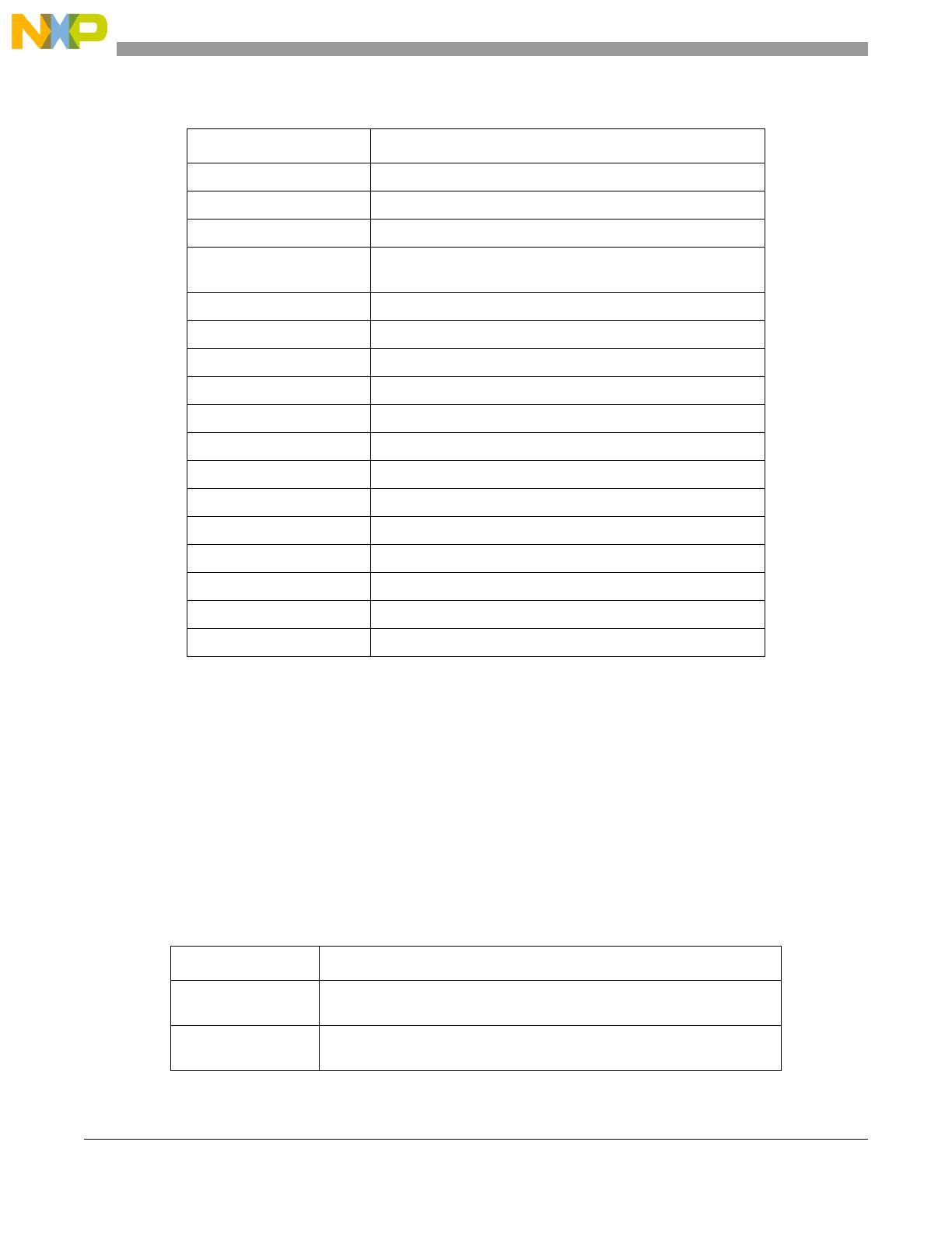
Table 4. DDR Features
DDR Feature Description
DDR3 Topology Each controller connects to its own SODIMM slot.
Supports write-leveling intended to help determine timing skews.
Termination All input signal lines are terminated at the DIMM modules.
Additional termination is not required.
Table 3. P5040/P5020 Pin Groupings Summary (continued)
Signal Group Details
P5040/P5020 Reference Design Board User Guide, Rev. 0
Freescale Semiconductor 9
Architecture
Figure 4. DDR interface
5.1.1.1 DDR Power
P5040/P5020RDB DDR power supplies these voltages.
The P5040/P5020RDB uses the Linear Technology LTC3876 (U55) switching power controller as
follows:
Dual-phase controller for up to 20 A at a default at 1.35 v adjustable to 1.5 V output.
Supplies GVDD, VREF, and VTT for SODIMM DRAM DDR3 and P5040/P5020 DDR controller.
Figure 5. DDR Power Supply
Voltage Name Voltage Current Note
GVDD 1.5V/1.35V > 10A DRAM core and IO
MVREF 0.75V/0.675V >= 10mA DRAM reference voltage
VTT 0.75V/0.675V >= 3A Bus termination supply
P5040/P5020 Reference Design Board User Guide, Rev. 0
10 Freescale Semiconductor
Architecture
The following summarizes the use of MECC pins on the P5040/P5020RDB:
RDB does not directly support MECC pin usage to access internal debug information. Since the
RDB does not provide a dedicated MUX, it has simpler routing and signal integrity status.
However, as the RDB does not interfere with the controller-to-DDR path, access to debug
information on MECC pins is possible by using a NextWave (or equivalent) DDR logic analyzer
connector and non-ECC DDR modules.
5.1.2 SerDes x20/x18 Interface
The SerDes block on the P5040/P5020 provides high-speed serial communications interfaces for several
internal devices. The SerDes block provides 20 or 18 serial lanes for the P5040 or P5020, respectively.
They may be partitioned as shown in Table 5(a) or (b), respectively.
Note that the term ‘lane’ is used to describe the minimum number of signals needed to create a
bidirectional communications channel; in the case of PCI-Express or Serial RapidIO, a lane consists of two
differential pairs, one for receive and one for transmit, or four in all.
Table 5, top down, shows the following clocking banks and how they are configured by the reference
board:
Bank1 Lanes A–D go to x4 slot 1, E is demuxed to either x1 slot 2 or combined with lanes
E-F to support 4 SGMII ports, and I–J to the Aurora debug connector
Bank2 Lanes A–D go to port 1 of dual-ported XAUI PHY
Bank3 Lanes A–B of P5040 goes to port 2 of dual-ported XAUI PHY while lanes C and
D of P5020 could be demuxed to either go to SATA ports 1 and 2 or go to port 2
of dual-ported XAUI PHY.
Bank 4 Lanes P1B and P2A of P5040 are muxed are with lanes C–D of P5020 to SATA
ports 1 and 2.
Table 5. P5040/P5020 SerDes Lane Multiplexing Configurations on P5040/P5020
Bank 1 Bank 2 Bank 3
Bank
4
ABCD E F G H I J A B C D A B C D
P1B
P2A
0 1 2 3 4 5 6 7 8 9 10 11 12 13 14 15 16 17
SLOT 1 SLOT 2
Aurora Conn on
SLOT 3
SATA
Port1
SATA
Port2
——
P5040 (RCW 02 and 34)
PCIe1
(5/2.5G)
PCIe2
(5/2.5G)
Debug (5/2.5G) XAUI FM1 XAUI FM2
SATA1
SATA2
PCIe1
(5/2.5G)
SGMII
FM2
SGMII
FM2
SGMII
FM2
SGMII
FM2
Debug (5/2.5G) XAUI FM2 ——SAT
A1
SAT
A2
——
P5020 (RCW 34 and 35)
P5040/P5020 Reference Design Board User Guide, Rev. 0
Freescale Semiconductor 11
Architecture
PCIe1
(5/2.5G)
PCIe2
(5/2.5G)
——Debug (5/2.5G) XAUI FM1
SATA1
SATA2
——
PCIe1
(5/2.5G)
SGMII
FM2
SGMII
FM2
SGMII
FM2
SGMII
FM2
Debug (5/2.5G) XAUI FM1 ——
SATA1
SATA2
——
Table 5. P5040/P5020 SerDes Lane Multiplexing Configurations on P5040/P5020 (continued)
Bank 1 Bank 2 Bank 3
Bank
4
ABCD E F G H I J A B C D A B C D
P1B
P2A
0 1 2 3 4 5 6 7 8 9 10 11 12 13 14 15 16 17
SLOT 1 SLOT 2
Aurora Conn on
SLOT 3
SATA
Port1
SATA
Port2
——
P5040/P5020 Reference Design Board User Guide, Rev. 0
12 Freescale Semiconductor
Architecture
Figure 6. P5040/P5020 SerDes Bank1 to Reference Board Cards/
Debug Connector Configuration
P5040/P5020
SD_TX/RX[0:3](p,n)
PEX Slot 1
TX/RX[0:3](p,n)
REFCLK_SD1(p,n)
100 MHz
PEX Slot 2
TX/RX[4:7](p,n)
Aurora Conn
TX/RX[1:0](p,n)
SD_TX/RX[4:7](p,n)
SD_TX/RX[8:9](p,n)
x4 PCIe Card
Aurora Debug
x1 PCIe card
x4 SGMII PHY
Connector
P5040/P5020 Reference Design Board User Guide, Rev. 0
Freescale Semiconductor 13
Architecture
Figure 7. P5040/P5020 SerDes Banks 2,3, and 4 to Reference Board XAUI ports/
SATA Connectors Configuration
5.1.3 Ethernet Controller (EC) Interfaces
The two TSEC—with twisted pair 10/100/1000-Base-T interface—are IEEE 802.3-compliant. Vitesse
VSC8244 PHY supports four integrated PHYs though only two are in use. The P5040/P5020RDB only
uses the RGMII protocol.
This table shows the general organization of the ETH system.
Table 6. 10/100/1000 Base-T GETH Ports
GETH Feature Specifics Description
GETH Clocks IDT
ICS8304AMLF
Low skew Fanout Buffer
Receives 125MHz clock oscillator input and generates four LVCMOS/LVTLL
outputs:
P5040/P5020 EC1_GTXCLK_125 clock input
P5040/P5020 EC2_GTXCLK_125 clock input
P5040/P5020 1588 clock input
VSC8244 PHY XTAL1 input
P5040/P5020
REFCLK_SD2/3/4(p,n)
125 MHz
Port 1 of TN8022
TX/RX[0:3](p,n)
SATA port1 & 2
TX/RX[1:2](p,n)
SD_TX/RX[10:13](p,n)
SD_TX/RX[14:17](p,n)
SATA connectors
2 COPPER PORTS
Port 2 of TN8022
p5040B3lanesA-D
p5020B3lanesCD
2 SFP+ PORTS
SD_TX/RX[P1B,P1A](p,n)
P5040/P5020 Reference Design Board User Guide, Rev. 0
14 Freescale Semiconductor
Architecture
GETH
Connectors
Copper Interface Integrated GETH RJ45 Connector for EC1 and USB TypeA connector for USB1
(J2)
•90
0
RJ45 connector for EC2 (P1)
PHY
Configuration
CMODE[7...0] Inputs used to configure VSC8244 hardware operating modes by connecting
Pull-up/down resistors.
PHY Default
Configuration
MAC interface select: RGMII to CAT5.
Speed/Duplex auto negotiation: 10/100/1000 Base-T HDX, FDX.
PHY address[4:2] = ’000’
PHY Control MII Management
Port
Controls the following via the two-wire interface port:
EMI1_MDC clock
EMI1_MDIO bi-directional data line
MAX4906 Analog switch that chooses EMI1 routing.
EMI1 Routing determined by one of the following:
P5040/P5020 GPIO[0...3]
ngPIXIS registers PX_BRDCFG1 and PX_BRDCFG2
PHY Reset VSC8244
PHY RESET
Input is driven by the P5040/P5020 HRESET
signal via FPGA, and reset after
each P5040/P5020 HRESET sequence.
Input can be driven by register PX_RST P5040/P5020RDB FPGA Bit 7.
VSC8244
SOFT_RESET
Input is driven by the P5040/P5020 HRESET
signal via FPGA, and reset after
each P5040/P5020 HRESET
sequence.
Input can be driven by register PX_RST P5040/P5020RDB FPGA Bit 5.
Can implement by asserting bit 15 (MSB) on VSC8244 PHY MII Mode Control
Register 0.
Table 6. 10/100/1000 Base-T GETH Ports (continued)
GETH Feature Specifics Description
P5040/P5020 Reference Design Board User Guide, Rev. 0
Freescale Semiconductor 15
Architecture
Figure 8. P5040/P5020 Ethernet Connections to the Reference Board
This table summarizes the reference board EC connections and routing when the board is populated with
a P5040 or P5020 processor.
See Section 5.1.9, “USB Interfaces.”
Table 7. P5040/P5020 Ethernet Port Locations on P5040/P5020
P5040/
P5020 EC #
Connection Port PHY Address Location
1 1 0 Conn. J6 top
2 2 1 Conn. P1
MI
CLKBUF
EC #2
EC #1
ENET PHY
1
2
GTXCLK
EC Port #1
USB Port #1
125 MHz
To USB1
EC Port #2
To 1588 Riser Card Connector
P5040/P5020
P5040/P5020 Reference Design Board User Guide, Rev. 0
16 Freescale Semiconductor
Architecture
5.1.4 Support for IEEE Std 1588
Protocol
The reference board supports the P5040/P5020 IEEE® 1588
precision time protocol (PTP) as shown in
Figure 9. This facility works in tandem with an Ethernet controller to timestamp incoming packets.
Figure 9. IEEE® 1588 Interface to Reference Board Symmetricon Riser Connector
5.1.5 Serial Interfaces
This figure shows overall connections of RS-232, eSPI, and eSDHC/eMMC interfaces.
TX >
P5040/P5020
STMP_TX/RX[1:2]
CLKIN
XTALOSC
125.000 MHz
±25 ppm
1588
CLKOUT
TRIGIN[1:2]
ALARMOUT[1:2]
Symmetricon
Riser Connector
PULSEOUT[1:2]
P5040/P5020 Reference Design Board User Guide, Rev. 0
Freescale Semiconductor 17
Architecture
Figure 10. Serial Interfaces
5.1.6 enhanced Serial Peripheral Interface (eSPI)
The P5040/P5020 has an eSPI Master Controller used to communicate with various peripherals.
Two SPI FLASH support 24-bit address and SPI Modes 0, 3.
Use Chip Select 0 or 1 with S25FL129P0XNFI001 FLASH if CVDD=3.3 V.
Use Chip Select 2 with 25AA1024T-I/SM FLASH for all CVDD voltages (1.8, 2.5, or 3.3 V).
Chip Select 3 is reserved for 1588 Riser Card.
This table describes the P5040/P5020RDB SPI FLASH memory.
P5040/P5020 Reference Design Board User Guide, Rev. 0
18 Freescale Semiconductor
Architecture
5.1.7 enhanced Secure Digital Host Controller (eSDHC) &
embedded Multi Media Controller (eMMC)
The P5040/P5020 processor has an eSDHC and an eMMC controller, which the P5040/P5020 connects to
an SD media card slot. The I
2
C3_SDA signal uses write protect (WP). The I
2
C3_SCL signal uses card
detect (CD). The DS supports the following:
1.8, 2.5, and 3.3V SD/eMMC media card voltages.
x4-bit and x8-bit cards though the latter uses SPI_CS[0:3] signals as eSDHC_DAT[4:7].
eSDHC_DAT[4:7] signals are shared with SPI CS pins.
Software can route the pins to either eSDHC/eMMC cards or SPI devices; however, they
cannot be used simultaneously.
CAUTION
Insert an SD/eMMC media card suited to P5040/P5020 CVDD voltage.
5.1.8 UART Serial Ports
Two RS-232 transceivers on the P5040/P5020RDB contribute to user application development and
provide convenient communication channels to both terminal and host computers. The transceivers are
connected to P5040/P5020 dedicated UART ports: one provides interconnection to DUT UART1/3 ports
or ngPIXIS FPGA; the other explores UART2/4 dedicated ports.
Analog Devices’ ADM561JRSZ product internally generates required RS-232 levels from 3.3V_HOT
supply.
NOTE
Powering from the 3.3V_HOT power rail is possible even when
P5040/P5020 is powered down. Thus, the FPGA processor can run
programs and interact with the user while allowing board reconfiguration
while sealed in the chassis.
This table describes the P5040/P5020RDB RS-232 interface.
Table 8. eSPI Slave devices
Device
Clock Frequency
(MHz)
Voltage Range (V) Capacity SPI CS
Spansion
S25FL129P0XNFI001
104 2.7–3.3 16 MB CS[0,1]
Microchip
25AA1024T-I/SM
2, 10, 20 1.8–3.3 128 KB CS2
1588 Riser Card 1.8–3.3 CS3
P5040/P5020 Reference Design Board User Guide, Rev. 0
Freescale Semiconductor 19
Architecture
5.1.9 USB Interfaces
The P5040/P5020 has dual HS USB transceivers whose main features are as follows:
Compliance with USB Specification, USB Rev. 2.0.
USB 2.0 Transceiver Macrocell Interface (UTMI) with Link Controller.
Supports HS, FS, and LS modes of operation.
Supports signalling.
Supports Host and Device modes.
Working in Host mode only, the RDB connects a USB transceiver to connector Type A thus
enabling communication with keyboards, mice, memory sticks, etc.
Working in Host and Device modes, a second USB transceiver connects to a second Type A
connector which has bus signal connecting directly to the P5040/P5020 internal PHY.
The 24MHz USB block reference clock provides additional control to the P5040/P5020 in conjunction
with the USB power sequence. GPIO 4,6 control the VBUS Drive. GPIO 5,7 get Power Fault indications
via the FPGA.
This figure shows the P5040/P5020RDB USB interface.
Table 9. P5040/P5020RDB RS232 Interface
UART Ports Destination Power supply Flow control External Connector
UART1 Terminal (Host
Computer)
3.3V_HOT Supported UART1/3 (J5 Bottom)
UART3 Unsupported
UART2 Supported UART2/4 (J5 Top)
UART4 Unsupported
P5040/P5020 Reference Design Board User Guide, Rev. 0
20 Freescale Semiconductor
Architecture
Figure 11. P5040/P5020 USB Connection to Reference Board USB Interfaces
5.1.10 DMA Controllers
The P5040/P5020 DMA controllers have internal and external controls to initiate and monitor DMA
activity. The reference board does not incorporate any specific devices that make use of the external
pin-controlled DMA controllers.
The P5040/P5020 DMA ports are connected to test points on the reference board to allow external
hardware control, as needed.
  • Page 1 1
  • Page 2 2
  • Page 3 3
  • Page 4 4
  • Page 5 5
  • Page 6 6
  • Page 7 7
  • Page 8 8
  • Page 9 9
  • Page 10 10
  • Page 11 11
  • Page 12 12
  • Page 13 13
  • Page 14 14
  • Page 15 15
  • Page 16 16
  • Page 17 17
  • Page 18 18
  • Page 19 19
  • Page 20 20
  • Page 21 21
  • Page 22 22
  • Page 23 23
  • Page 24 24
  • Page 25 25
  • Page 26 26
  • Page 27 27
  • Page 28 28
  • Page 29 29
  • Page 30 30
  • Page 31 31
  • Page 32 32
  • Page 33 33
  • Page 34 34
  • Page 35 35
  • Page 36 36
  • Page 37 37
  • Page 38 38
  • Page 39 39
  • Page 40 40
  • Page 41 41
  • Page 42 42
  • Page 43 43
  • Page 44 44
  • Page 45 45
  • Page 46 46
  • Page 47 47
  • Page 48 48
  • Page 49 49
  • Page 50 50
  • Page 51 51
  • Page 52 52
  • Page 53 53
  • Page 54 54
  • Page 55 55
  • Page 56 56
  • Page 57 57
  • Page 58 58
  • Page 59 59
  • Page 60 60
  • Page 61 61
  • Page 62 62
  • Page 63 63
  • Page 64 64
  • Page 65 65
  • Page 66 66
  • Page 67 67
  • Page 68 68
  • Page 69 69
  • Page 70 70
  • Page 71 71
  • Page 72 72
  • Page 73 73
  • Page 74 74
  • Page 75 75
  • Page 76 76
  • Page 77 77

NXP P5010 User manual

Category
Water pumps
Type
User manual
This manual is also suitable for

Ask a question and I''ll find the answer in the document

Finding information in a document is now easier with AI