
BG95 Hardware Design
LPWA Module Series
Rev. BG95_Hardware_Design_V1.0
Date: 2019-05-15
Status: Preliminary
www.quectel.com

LPWA Module Series
BG95 Hardware Design
BG95_Hardware_Design 1 / 80
Our aim is to provide customers with timely and comprehensive service. For any
assistance, please contact our company headquarters:
Quectel Wireless Solutions Co., Ltd.
7
th
Floor, Hongye Building, No.1801 Hongmei Road, Xuhui District, Shanghai 200233, China
Tel: +86 21 5108 6236
Email: [email protected]
Or our local office. For more information, please visit:
http://www.quectel.com/support/sales.htm
For technical support, or to report documentation errors, please visit:
http://www.quectel.com/support/technical.htm
Or email to: [email protected]
GENERAL NOTES
QUECTEL OFFERS THE INFORMATION AS A SERVICE TO ITS CUSTOMERS. THE INFORMATION
PROVIDED IS BASED UPON CUSTOMERS’ REQUIREMENTS. QUECTEL MAKES EVERY EFFORT
TO ENSURE THE QUALITY OF THE INFORMATION IT MAKES AVAILABLE. QUECTEL DOES NOT
MAKE ANY WARRANTY AS TO THE INFORMATION CONTAINED HEREIN, AND DOES NOT ACCEPT
ANY LIABILITY FOR ANY INJURY, LOSS OR DAMAGE OF ANY KIND INCURRED BY USE OF OR
RELIANCE UPON THE INFORMATION. ALL INFORMATION SUPPLIED HEREIN IS SUBJECT TO
CHANGE WITHOUT PRIOR NOTICE.
COPYRIGHT
THE INFORMATION CONTAINED HERE IS PROPRIETARY TECHNICAL INFORMATION OF
QUECTEL WIRELESS SOLUTIONS CO., LTD. TRANSMITTING, REPRODUCTION, DISSEMINATION
AND EDITING OF THIS DOCUMENT AS WELL AS UTILIZATION OF THE CONTENT ARE
FORBIDDEN WITHOUT PERMISSION. OFFENDERS WILL BE HELD LIABLE FOR PAYMENT OF
DAMAGES. ALL RIGHTS ARE RESERVED IN THE EVENT OF A PATENT GRANT OR
REGISTRATION OF A UTILITY MODEL OR DESIGN.
Copyright © Quectel Wireless Solutions Co., Ltd. 2019. All rights reserved.

LPWA Module Series
BG95 Hardware Design
BG95_Hardware_Design 2 / 80
About the Document
History
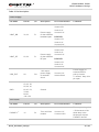
Revision Date Author Description
1.0 2019-05-15
Lim PENG/
Garey XIE
Initial

LPWA Module Series
BG95 Hardware Design
BG95_Hardware_Design 3 / 80
Contents
About the Document ................................................................................................................................ 2
Contents .................................................................................................................................................... 3
Table Index ............................................................................................................................................... 5
Figure Index .............................................................................................................................................. 7
1 Introduction ....................................................................................................................................... 8
1.1. Safety Information .................................................................................................................... 9
2 Product Concept ............................................................................................................................. 13
2.1. General Description ................................................................................................................ 13
2.2. Key Features .......................................................................................................................... 15
2.3. Functional Diagram ................................................................................................................ 18
2.4. Evaluation Board .................................................................................................................... 19
3 Application Interfaces ..................................................................................................................... 20
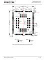
3.1. Pin Assignment ...................................................................................................................... 21
3.2. Pin Description ....................................................................................................................... 22
3.3. Operating Modes .................................................................................................................... 29
3.4. Power Saving ......................................................................................................................... 30
3.4.1. Airplane Mode .............................................................................................................. 30
3.4.2. Power Saving Mode (PSM).......................................................................................... 31
3.4.3. Extended Idle Mode DRX (e-I-DRX) ............................................................................ 32
3.4.4. Sleep Mode* ................................................................................................................ 32
3.4.4.1. UART Application .............................................................................................. 32
3.5. Power Supply ......................................................................................................................... 33
3.5.1. Power Supply Pins ....................................................................................................... 33
3.5.2. Decrease Voltage Drop ............................................................................................... 34
3.5.3. Monitor the Power Supply ............................................................................................ 35
3.6. Turn on and off Scenarios ...................................................................................................... 35
3.6.1. Turn on Module Using the PWRKEY Pin ..................................................................... 35
3.6.2. Turn off Module ............................................................................................................ 37
3.6.2.1. Turn off Module Using the PWRKEY Pin ........................................................... 37
3.6.2.2. Turn off Module Using AT Command ................................................................ 38
3.7. Reset the Module ................................................................................................................... 38
3.8. (U)SIM Interface ..................................................................................................................... 40
3.9. USB Interface ......................................................................................................................... 42
3.10. UART Interfaces ..................................................................................................................... 44
3.11. PCM* and I2C* Interfaces ......................................................................................................
47
3.12. Network Status Indication ....................................................................................................... 48
3.13. STATUS ................................................................................................................................. 49
3.14. Behaviors of RI* ..................................................................................................................... 49
3.15. USB_BOOT Interface ............................................................................................................. 50
3.16. ADC Interfaces ....................................................................................................................... 51

LPWA Module Series
BG95 Hardware Design
BG95_Hardware_Design 4 / 80
3.17. GPIO Interfaces ...................................................................................................................... 52
4 GNSS Receiver ................................................................................................................................ 54
4.1. General Description ................................................................................................................ 54
4.2. GNSS Performance ................................................................................................................ 54
4.3. Layout Guidelines ................................................................................................................... 55
5 Antenna Interfaces .......................................................................................................................... 56
5.1. Main Antenna Interface .......................................................................................................... 56
5.1.1. Pin Definition ................................................................................................................ 56
5.1.2. Operating Frequency ................................................................................................... 56
5.1.3. Reference Design of RF Antenna Interface ................................................................. 57
5.1.4. Reference Design of RF Layout ................................................................................... 58
5.2. GNSS Antenna Interface ........................................................................................................ 60
5.3. Antenna Installation ................................................................................................................ 61
5.3.1. Antenna Requirements ................................................................................................ 61
5.3.2. Recommended RF Connector for Antenna Installation ................................................ 62
6 Electrical, Reliability and Radio Characteristics .......................................................................... 64
6.1. Absolute Maximum Ratings .................................................................................................... 6
4
6.2. Power Supply Ratings ............................................................................................................ 64
6.3. Operation and Storage Temperatures .................................................................................... 65
6.4. RF Output Power .................................................................................................................... 65
6.5. RF Receiving Sensitivity ......................................................................................................... 66
6.6. Electrostatic Discharge ........................................................................................................... 67
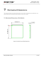
7 Mechanical Dimensions.................................................................................................................. 69
7.1. Mechanical Dimensions of the Module ................................................................................... 69
7.2. Recommended Footprint ........................................................................................................ 71
7.3. Design Effect Drawings of the Module .................................................................................... 72
8 Storage, Manufacturing and Packaging ........................................................................................ 73
8.1. Storage ................................................................................................................................... 73
8.2. Manufacturing and Soldering .................................................................................................. 74
8.3. Packaging ............................................................................................................................... 75
9 Appendix A References .................................................................................................................. 77
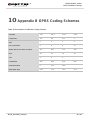
10 Appendix B GPRS Coding Schemes ............................................................................................. 80
11 Appendix C GPRS Multi-slot Classes ............................................................................................
81
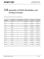
12 Appendix D EDGE Modulation and Coding Schemes .................................................................. 83

LPWA Module Series
BG95 Hardware Design
BG95_Hardware_Design 5 / 80
Table Index
TABLE 1: VERSION SELECTION FOR BG95 SERIES MODULE ................................................................... 13
TABLE 2: FREQUENCY BANDS AND GNSS TYPES OF BG95 SERIES MODULE ...................................... 13
TABLE 3: KEY FEATURES OF BG95 SERIES MODULES ............................................................................. 16
TABLE 4: DEFINITION OF I/O PARAMETERS ................................................................................................ 22
TABLE 5: PIN DESCRIPTION ........................................................................................................................... 23
TABLE 6: OVERVIEW OF OPERATING MODES ............................................................................................ 30
TABLE 7: VBAT AND GND PINS ...................................................................................................................... 34
TABLE 8: PIN DEFINITION OF PWRKEY ........................................................................................................ 36
TABLE 9: PIN DEFINITION OF RESET_N ....................................................................................................... 38
TABLE 10: PIN DEFINITION OF (U)SIM INTERFACE ..................................................................................... 40
TABLE 11: PIN DEFINITION OF USB INTERFACE ......................................................................................... 42
TABLE 12: PIN DEFINITION OF MAIN UART INTERFACE ............................................................................ 44
TABLE 13: PIN DEFINITION OF DEBUG UART INTERFACE......................................................................... 45
TABLE 14: PIN DEFINITION OF GNSS UART INTERFACE ........................................................................... 45
TABLE 15: LOGIC LEVELS OF DIGITAL I/O ................................................................................................... 45
TABLE 16: PIN DEFINITION OF PCM AND I2C INTERFACES ...................................................................... 47
TABLE 17: PIN DEFINITION OF NETLIGHT .................................................................................................... 48
TABLE 18: WORKING STATE OF NETLIGHT ................................................................................................. 48
TABLE 19: PIN DEFINITION OF STATUS ....................................................................................................... 49
TABLE 20: DEFAULT BEHAVIORS OF RI ....................................................................................................... 50
TABLE 21: PIN DEFINITION OF USB_BOOT INTERFACE............................................................................. 50
TABLE 22: PIN DEFINITION OF ADC INTERFACE ......................................................................................... 51
TABLE 23: CHARACTERISTICS OF ADC INTERFACES ................................................................................ 52
TABLE 24: PIN DEFINITION OF GPIO INTERFACES ..................................................................................... 52
TABLE 25: LOGIC LEVELS OF GPIO INTERFACES ...................................................................................... 53
TABLE 26: GNSS PERFORMANCE ................................................................................................................. 54
TABLE 27: PIN DEFINITION OF MAIN ANTENNA INTERFACE ..................................................................... 56
TABLE 28: BG95 OPERATING FREQUENCY ................................................................................................. 56
TABLE 29: PIN DEFINITION OF GNSS ANTENNA INTERFACE .................................................................... 60
TABLE 30: GNSS FREQUENCY ...................................................................................................................... 60
TABLE 31: ANTENNA REQUIREMENTS ......................................................................................................... 61
TABLE 32: ABSOLUTE MAXIMUM RATINGS ................................................................................................. 64
TABLE 33: POWER SUPPLY RATINGS .......................................................................................................... 64
TABLE 34: OPERATION AND STORAGE TEMPERATURES ......................................................................... 65
TABLE 35: BG95 RF OUTPUT POWER ........................................................................................................... 66
TABLE 36: BG95 CONDUCTED RF RECEIVING SENSITIVITY ..................................................................... 66
TABLE 37: ELECTROSTATIC DISCHARGE CHARACTERISTICS (25ºC, 45% RELATIVE HUMIDITY) ....... 68
TABLE 38: RECOMMENDED THERMAL PROFILE PARAMETERS .............................................................. 74
TABLE 39: REEL PACKAGING ........................................................................................................................ 76
TABLE 40: RELATED DOCUMENTS ............................................................................................................... 77
TABLE 41: TERMS AND ABBREVIATIONS ..................................................................................................... 77

LPWA Module Series
BG95 Hardware Design
BG95_Hardware_Design 6 / 80
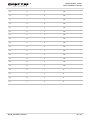
TABLE 42: DESCRIPTION OF DIFFERENT CODING SCHEMES .................................................................. 80
TABLE 43: GPRS MULTI-SLOT CLASSES ...................................................................................................... 81
TABLE 44: EDGE MODULATION AND CODING SCHEMES .......................................................................... 83

LPWA Module Series
BG95 Hardware Design
BG95_Hardware_Design 7 / 80
Figure Index
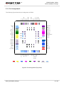
FIGURE 1: FUNCTIONAL DIAGRAM ............................................................................................................... 18
FIGURE 2: PIN ASSIGNMENT (TOP VIEW) .................................................................................................... 21
FIGURE 3: SLEEP MODE APPLICATION VIA UART ...................................................................................... 33
FIGURE 4: POWER SUPPLY LIMITS DURING BURST TRANSMISSION ..................................................... 34
FIGURE 5: STAR STRUCTURE OF THE POWER SUPPLY ........................................................................... 35
FIGURE 6: TURN ON THE MODULE USING DRIVING CIRCUIT ................................................................... 36
FIGURE 7: TURN ON THE MODULE USING KEYSTROKE ........................................................................... 36
FIGURE 8: TIMING OF TURNING ON MODULE ............................................................................................. 37
FIGURE 9: TIMING OF TURNING OFF MODULE ........................................................................................... 38
FIGURE 10: TIMING OF RESET MODULE ...................................................................................................... 39
FIGURE 11: REFERENCE CIRCUIT OF RESET_N BY USING DRIVING CIRCUIT ...................................... 39
FIGURE 12: REFERENCE CIRCUIT OF RESET_N BY USING BUTTON ...................................................... 39
FIGURE 13: REFERENCE CIRCUIT OF (U)SIM INTERFACE WITH AN 8-PIN (U)SIM CARD CONNECTOR
................................................................................................................................................................... 41
FIGURE 14: REFERENCE CIRCUIT OF (U)SIM INTERFACE WITH A 6-PIN (U)SIM CARD CONNECTOR 41
FIGURE 15: REFERENCE CIRCUIT OF USB INTERFACE ............................................................................ 43
FIGURE 16: REFERENCE CIRCUIT WITH TRANSLATOR CHIP ................................................................... 46
FIGURE 17: REFERENCE CIRCUIT WITH TRANSISTOR CIRCUIT .............................................................. 46
FIGURE 18: REFERENCE CIRCUIT OF PCM APPLICATION WITH AUDIO CODEC ................................... 47
FIGURE 19: REFERENCE CIRCUIT OF THE NETWORK STATUS INDICATOR .......................................... 48
FIGURE 20: REFERENCE CIRCUIT OF STATUS ........................................................................................... 49
FIGURE 21: REFERENCE CIRCUIT OF USB_BOOT INTERFACE ................................................................ 51
FIGURE 22: REFERENCE CIRCUIT OF RF ANTENNA INTERFACE ............................................................ 58
FIGURE 23: MICROSTRIP LINE DESIGN ON A 2-LAYER PCB ..................................................................... 58
FIGURE 24: COPLANAR WAVEGUIDE LINE DESIGN ON A 2-LAYER PCB ................................................. 59
FIGURE 25: COPLANAR WAVEGUIDE LINE DESIGN ON A 4-LAYER PCB (LAYER 3 AS REFERENCE
GROUND) .................................................................................................................................................. 59
FIGURE 26: COPLANAR WAVEGUIDE LINE DESIGN ON A 4-LAYER PCB (LAYER 4 AS REFERENCE
GROUND) .................................................................................................................................................. 59
FIGURE 27: REFERENCE CIRCUIT OF GNSS ANTENNA INTERFACE ....................................................... 61
FIGURE 28: DIMENSIONS OF THE U.FL-R-SMT CONNECTOR (UNIT: MM) ............................................... 62
FIGURE 29: MECHANICALS OF U.FL-LP CONNECTORS ............................................................................. 63
FIGURE 30: SPACE FACTOR OF MATED CONNECTOR (UNIT: MM) .......................................................... 63
FIGURE 31: MODULE TOP AND SIDE DIMENSIONS .................................................................................... 69
FIGURE 32: MODULE BOTTOM DIMENSIONS (BOTTOM VIEW) ................................................................. 70
FIGURE 33: RECOMMENDED FOOTPRINT (TOP VIEW) .............................................................................. 71
FIGURE 34: TOP VIEW OF THE MODULE ...................................................................................................... 72
FIGURE 35: BOTTOM VIEW OF THE MODULE .............................................................................................. 72
FIGURE 36: RECOMMENDED REFLOW SOLDERING THERMAL PROFILE ............................................... 74
FIGURE 37: TAPE DIMENSIONS ..................................................................................................................... 75
FIGURE 38: REEL DIMENSIONS ..................................................................................................................... 76

LPWA Module Series
BG95 Hardware Design
BG95_Hardware_Design 8 / 80
1 Introduction
This document defines BG95 module and describes its air interface and hardware interfaces which are
connected with customers’ applications.
This document can help customers quickly understand the interface specifications, electrical and
mechanical details, as well as other related information of BG95. To facilitate its application in different
fields, reference design is also provided for customers’ reference. Associated with application notes and
user guides, customers can use the module to design and set up mobile applications easily.

LPWA Module Series
BG95 Hardware Design
BG95_Hardware_Design 9 / 80
1.1. Safety Information
The following safety precautions must be observed during all phases of the operation, such as usage,
service or repair of any cellular terminal or mobile incorporating BG95. Manufacturers of the cellular
terminal should send the following safety information to users and operating personnel, and incorporate
these guidelines into all manuals supplied with the product. If not so, Quectel assumes no liability for
customers’ failure to comply with these precautions.
Full attention must be given to driving at all times in order to reduce the risk of an
accident. Using a mobile while driving (even with a handsfree kit) causes
distraction and can lead to an accident. Please comply with laws and regulations
restricting the use of wireless devices while driving.
Switch off the cellular terminal or mobile before boarding an aircraft. The operation
of wireless appliances in an aircraft is forbidden to prevent interference with
communication systems. If the device offers an Airplane Mode, then it should be
enabled prior to boarding an aircraft. Please consult the airline staff for more
restrictions on the use of wireless devices on boarding the aircraft.
Wireless devices may cause interference on sensitive medical equipment, so
please be aware of the restrictions on the use of wireless devices when in
hospitals, clinics or other healthcare facilities.
Cellular terminals or mobiles operating over radio signals and cellular network
cannot be guaranteed to connect in all possible conditions (for example, with
unpaid bills or with an invalid (U)SIM card). When emergent help is needed in such
conditions, please remember using emergency call. In order to make or receive a
call, the cellular terminal or mobile must be switched on in a service area with
adequate cellular signal strength.
The cellular terminal or mobile contains a transmitter and receiver. When it is ON, it
receives and transmits radio frequency signals. RF interference can occur if it is
used close to TV set, radio, computer or other electric equipment.
In locations with potentially explosive atmospheres, obey all posted signs to turn
off wireless devices such as your phone or other cellular terminals. Areas with
potentially explosive atmospheres include fueling areas, below decks on boats,
fuel or chemical transfer or storage facilities, areas where the air contains
chemicals or particles such as grain, dust or metal powders, etc.

LPWA Module Series
BG95 Hardware Design
BG95_Hardware_Design 10 / 80
1.2. FCC Certification Requirements.
According to the definition of mobile and fixed device is described in Part 2.1091(b), this device is a
mobile device.
And the following conditions must be met:
1. This Modular Approval is limited to OEM installation for mobile and fixed applications only. The antenna
installation and operating configurations of this transmitter, including any applicable source-based time-
averaging duty factor, antenna gain and cable loss must satisfy MPE categorical Exclusion Requirements
of 2.1091.
2. The EUT is a mobile device; maintain at least a 20 cm separation between the EUT and the user’s
body and must not transmit simultaneously with any other antenna or transmitter.
3.A label with the following statements must be attached to the host end product: This device contains
FCC ID: XMR201910BG96M3.
4.To comply with FCC regulations limiting both maximum RF output power and human exposure to RF
radiation, maximum antenna gain (including cable loss) must not exceed:
❒ GSM850:≤8.571 dBi
❒ GSM1900:≤10.030dBi
❒ Catm LTE Band2/25:≤11.000dBi
❒ Catm LTE Band4/66:≤8.000dBi
❒ Catm LTE Band5/26:≤12.541dBi
❒ Catm LTE Band12/85:≤11.798dBi
❒ Catm LTE Band13:≤12.214dBi
❒ Catm LTE Band14:≤12.272 dBi
❒ NB LTE Band2/25:≤11.000dBi
❒ NB LTE Band4/66:≤8.000dBi
❒ NB LTE Band5/26:≤12.541dBi
❒ NB LTE Band12/85:≤11.798dBi
❒ NB LTE Band13:≤12.214dBi
❒ BNLTE Band14:≤12.272 dBi

LPWA Module Series
BG95 Hardware Design
BG95_Hardware_Design 11 / 80
❒NB LTE Band71:≤11.687 dBi
5. This module must not transmit simultaneously with any other antenna or transmitter
6. The host end product must include a user manual that clearly defines operating requirements and
conditions that must be observed to ensure compliance with current FCC RF exposure guidelines.
For portable devices, in addition to the conditions 3 through 6 described above, a separate approval is
required to satisfy the SAR requirements of FCC Part 2.1093
If the device is used for other equipment that separate approval is required for all other operating
configurations, including portable configurations with respect to 2.1093 and different antenna
configurations.
For this device, OEM integrators must be provided with labeling instructions of finished products.
Please refer to KDB784748 D01 v07, section 8. Page 6/7 last two paragraphs:
A certified modular has the option to use a permanently affixed label, or an electronic label. For a
permanently affixed label, the module must be labeled with an FCC ID - Section 2.926 (see 2.2
Certification (labeling requirements) above). The OEM manual must provide clear instructions
explaining to the OEM the labeling requirements, options and OEM user manual instructions that are
required (see next paragraph).
For a host using a certified modular with a standard fixed label, if (1) the module’s FCC ID is not visible
when installed in the host, or (2) if the host is marketed so that end users do not have straightforward
commonly used methods for access to remove the module so that the FCC ID of the module is visible;
then an additional permanent label referring to the enclosed module:“Contains Transmitter Module
FCC ID: XMR201910BG96M3” or “Contains FCC ID: XMR201910BG96M3” must be used. The host
OEM user manual must also contain clear instructions on how end users can find and/or access the
module and the FCC ID.

LPWA Module Series
BG95 Hardware Design
BG95_Hardware_Design 12 / 80
The final host / module combination may also need to be evaluated against the FCC Part 15B criteria
for unintentional radiators in order to be properly authorized for operation as a Part 15 digital device.
The user’s manual or instruction manual for an intentional or unintentional radiator shall caution the
user that changes or modifications not expressly approved by the party responsible for compliance
could void the user's authority to operate the equipment. In cases where the manual is provided only in
a form other than paper, such as on a computer disk or over the Internet, the information required by
this section may be included in the manual in that alternative form, provided the user can reasonably be
expected to have the capability to access information in that form.
This device complies with part 15 of the FCC Rules. Operation is subject to the following two conditions:
(1) This device may not cause harmful interference, and (2) this device must accept any interference
received, including interference that may cause undesired operation.
Changes or modifications not expressly approved by the manufacturer could void the user’s authority to
operate the equipment.

LPWA Module Series
BG95 Hardware Design
BG95_Hardware_Design 13 / 80
2 Product Concept
2.1. General Description
BG95 is a series of embedded IoT (LTE Cat M1, LTE Cat NB2 and EGPRS) wireless communication
module. It provides data connectivity on LTE-FDD/GPRS/EGPRS networks, and supports half-duplex
operation in LTE networks. It also provides GNSS
1)
and voice
2)
functionality to meet customers’ specific
application demands.
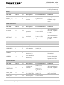
Table 1: Version Selection for BG95 Series Module
Table 2: Frequency Bands and GNSS Types of BG95 Series Module
Version Cat M1 VoLTE
Cat NB2
3)
/
NB1
GSM
Wi-Fi
Positioning
GNSS
(Optional)
BG95-M1
Y Y N N N Y
BG95-M2*
Y Y Y N N Y
BG95-M3*
Y Y Y Y N Y
BG95-N1*
N N Y N N Y
BG95-M4
4)
Y Y Y N N Y
BG95-M5
4)
Y Y Y N N Y
BG95-MF
4)
Y Y Y N Y Y
Module Supported Bands LTE Bands Power Class GNSS (Optional)
BG95-M1
Cat M1 Only:
LTE-FDD:
B1/B2/B3/B4/B5/B8/B12/B13/
B14/B18/B19/B20/B25/B26*/B27/
B28/B66/B85
Power Class 5 (20dBm)
GPS,
GLONASS, BeiDou,
Galileo

LPWA Module Series
BG95 Hardware Design
BG95_Hardware_Design 14 / 80
BG95-M2*
Cat M1:
LTE-FDD:
B1/B2/B3/B4/B5/B8/B12/B13/
B14/B18/B19/B20/B25/B26*/
B27/B28/B66/B85
Cat NB2:
LTE-FDD:
B1/B2/B3/B4/B5/B8/B12/B13/
B18/B19/B20/B25/B26*/B28/B66/
B71/B85
Power Class 5 (20dBm)
GPS,
GLONASS, BeiDou,
Galileo
BG95-M3*
Cat M1:
LTE-FDD:
B1/B2/B3/B4/B5/B8/B12/B13/
B14/B18/B19/B20/B25/B26*/B27/
B28/B66/B85
Cat NB2:
LTE-FDD:
B1/B2/B3/B4/B5/B8/B12/B13/
B18/B19/B20/B25/B26*/
B28/B66/B71/B85
EGPRS:
850/900/1800/1900MHz
Power Class 5 (20dBm)
GPS,
GLONASS, BeiDou,
Galileo
BG95-N1*
Cat NB2
Only:
LTE FDD:
B1/B2/B3/B4/B5/B8/B12/B13/
B18/B19/B20/B25/B26*/
B28/B66/B71/B85
Power Class 5 (20dBm)
GPS,
GLONASS, BeiDou,
Galileo
BG95-M4
4)
Cat M1:
LTE-FDD:
B1/B2/B3/B4/B5/B8/B12/B13/
B14/B18/B19/B20/B25/B26/B27/
B28/B31/B66/B72/B73/B85
Cat NB2:
LTE-FDD:
B1/B2/B3/B4/B5/B8/B12/B13/
B18/B19/B20/B25/B26/B28/B31/
B66/B72/B73/B85
Power Class 5 (20dBm)
GPS,
GLONASS, BeiDou,
Galileo
BG95-M5
4)
Cat M1:
LTE-FDD:
B1/B2/B3/B4/B5/B8/B12/B13/
B14/B18/B19/B20/B25/B26/B27/
B28/B66/B85
Cat NB2:
LTE-FDD:
Power Class 3 (23dBm)
GPS,
GLONASS, BeiDou,
Galileo

LPWA Module Series
BG95 Hardware Design
BG95_Hardware_Design 15 / 80
1.
1)
GNSS function is optional.
2.
2)
BG95 series module supports VoLTE (Voice over LTE) under LTE Cat M1 and CS voice under
GSM.
3.
3)
LTE Cat NB2 is backward compatible with LTE Cat NB1.
4.
4)
BG95-M4/-M5/-MF are still under planning. Therefore, details of them are currently not included
and will be added in a future release of this document.
5. “*” means under development.
With a compact profile of 23.6mm × 19.9mm × 2.2mm, BG95 can meet almost all requirements for M2M
applications such as smart metering, tracking system, security, wireless POS, etc.
BG95 is an SMD type module which can be embedded into applications through its 102 LGA pads. It
supports internet service protocols like TCP, UDP and PPP. Extended AT commands have been
developed for customers to use these internet service protocols easily.
2.2. Key Features
The following table describes the detailed features of BG95 series modules.
B1/B2/B3/B4/B5/B8/B12/B13/
B18/B19/B20/B25/B26/B28/B66/
B71/B85
BG95-MF
4)
Cat M1:
LTE-FDD:
B1/B2/B3/B4/B5/B8/B12/B13/
B14/B18/B19/B20/B25/B26/B27/
B28/B66/B85
Cat NB2:
LTE-FDD:
B1/B2/B3/B4/B5/B8/B12/B13/
B18/B19/B20/B25/B26/
B28/B66/B71/B85
Wi-Fi (For Positioning Only):
2.4GHz/5GHz
Power Class 5 (20dBm)
GPS,
GLONASS, BeiDou,
Galileo
NOTES

LPWA Module Series
BG95 Hardware Design
BG95_Hardware_Design 16 / 80
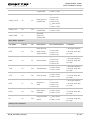
Table 3: Key Features of BG95 Series Modules
Features Details
Power Supply
BG95-M1/-M2/-N1:
Supply voltage: 2.4V~4.8V
Typical supply voltage: 3.3V
BG95-M3:
Supply voltage: 3.3V~4.3V
Typical supply voltage: 3.8V
Transmitting Power
Class 5 (20dBm±2dB) for LTE-FDD bands
Class 4 (33dBm±2dB) for GSM850
Class 4 (33dBm±2dB) for EGSM900
Class 1 (30dBm±2dB) for DCS1800
Class 1 (30dBm±2dB) for PCS1900
Class E2 (27dBm±3dB) for GSM850 8-PSK
Class E2 (27dBm±3dB) for EGSM900 8-PSK
Class E2 (26dBm±3dB) for DCS1800 8-PSK
Class E2 (26dBm±3dB) for PCS1900 8-PSK
LTE Features
Support LTE Cat M1 and LTE Cat NB2
Support 1.4MHz RF bandwidth for LTE Cat M1
Support 200KHz RF bandwidth for LTE Cat NB2
Support SISO in DL direction
Cat M1: Max. 589Kbps (DL)/1.12Mbps (UL)
Cat NB2: Max. 136Kbps (DL)/150Kbps (UL)
GSM Features
GPRS:
Support GPRS multi-slot class 33 (33 by default)
Coding scheme: CS-1, CS-2, CS-3 and CS-4
Max. 107Kbps (DL), Max. 85.6Kbps (UL)
EDGE:
Support EDGE multi-slot class 33 (33 by default)
Support GMSK and 8-PSK for different MCS (Modulation and Coding
Scheme)
Downlink coding schemes: CS 1-4 and MCS 1-9
Uplink coding schemes: CS 1-4 and MCS 1-9
Max. 296Kbps (DL), Max. 236.8Kbps (UL)
Internet Protocol
Features*
Support PPP/TCP/UDP/SSL/TLS/FTP(S)/HTTP(S)/NITZ/PING/MQTT/
CoAP protocols
Support PAP (Password Authentication Protocol) and CHAP (Challenge
Handshake Authentication Protocol) protocols which are usually used for
PPP connections
SMS
Text and PDU mode
Point to point MO and MT
SMS cell broadcast

LPWA Module Series
BG95 Hardware Design
BG95_Hardware_Design 17 / 80
1. “*” means under development.
2.
1)
Within operation temperature range, the module is 3GPP compliant.
3.
2)
Within extended temperature range, the module remains the ability to establish and maintain a
voice, SMS, data transmission, emergency call, etc. There is no unrecoverable malfunction. There
SMS storage: ME by default
(U)SIM Interface Support 1.8V USIM/SIM card
Audio Feature* Support one digital audio interface: PCM interface
USB Interface
Compliant with USB 2.0 specification (slave only)
Support operations at low-speed and full-speed
Used for AT command communication, data transmission, GNSS NMEA
output, software debugging and firmware upgrade
Support USB serial drivers for Windows 7/8/8.1/10, Linux 2.6/3.x (3.4 or
later)/4.1~4.15, Android 4.x/5.x/6.x/7.x/8.x/9.x
UART Interfaces
Main UART:
Used for data transmission and AT command communication
115200bps baud rate by default
The default frame format is 8N1 (8 data bits, no parity, 1 stop bit)
Support RTS and CTS hardware flow control
Debug UART:
Used for software debugging and log output
Support 115200bps baud rate
GNSS UART:
Used for GNSS data and NMEA sentences output
115200bps baud rate by default
AT Commands
3GPP TS 27.007 and 3GPP TS 27.005 AT commands, as well as Quectel
enhanced AT commands
Network Indication One NETLIGHT pin for network connectivity status indication
Antenna Interfaces
Including main antenna (ANT_MAIN) and GNSS antenna (ANT_GNSS)
interfaces
Physical Characteristics
Size: (23.6±0.15)mm × (19.9±0.15)mm × (2.2±0.2)mm
Weight: approx. 2.15g
Temperature Range
Operation temperature range: -35°C ~ +75°C
1)
Extended temperature range: -40°C ~ +85°C
2)
Storage temperature range: -40°C ~ +90°C
Firmware Upgrade USB interface, DFOTA*
RoHS All hardware components are fully compliant with EU RoHS directive
NOTES

LPWA Module Series
BG95 Hardware Design
BG95_Hardware_Design 18 / 80
are also no effects on radio spectrum and no harm to radio network. Only one or more parameters like
P
out
might reduce in their value and exceed the specified tolerances. When the temperature returns to
the normal operating temperature levels, the module will meet 3GPP specifications again.
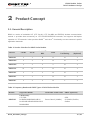
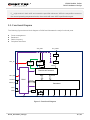
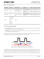
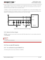
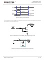
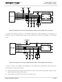
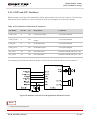
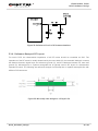
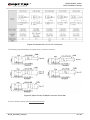
2.3. Functional Diagram
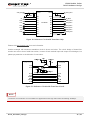
The following figure shows a block diagram of BG95 and illustrates the major functional parts.
Power management
Baseband
Radio frequency
Peripheral interfaces
Baseband
PMIC
Transceiver/PA/switch
SAW
ANT_MAIN
ANT_GNSS
VBAT_BB
VBAT_RF
PWRKEY
VDD_EXT
USB
(U)SIM PCM*
I2C*
19.2M
XO
GPIOs
Control
IQ Control
LNA
Tx
Rx
GNSS
UARTs
PA
(GSM)
ADC0
(ASM)
STATUS NETLIGHT
eSIM
RESET_N
ADC1
Figure 1: Functional Diagram

LPWA Module Series
BG95 Hardware Design
BG95_Hardware_Design 19 / 80
1. eSIM function is optional. If eSIM is selected, then the external (U)SIM cannot be used
simultaneously.
2. RESET_N will be supported in the next hardware design version.
3. ADC0 and ADC1 cannot be used simultaneously. BG95 supports using of only one ADC interface at a
time: either ADC0 or ADC1. Currently only ADC0 is enabled, and ADC1 will be enabled in the next
hardware design version.
4. “*” means under development.
2.4. Evaluation Board
In order to help customers to develop applications conveniently with BG95, Quectel supplies the
evaluation board (EVB), USB to RS-232 converter cable, USB data cable, earphone, antenna and other
peripherals to control or test the module. For more details, please refer to document [1].
NOTES
Page is loading ...
Page is loading ...
Page is loading ...
Page is loading ...
Page is loading ...
Page is loading ...
Page is loading ...
Page is loading ...
Page is loading ...
Page is loading ...
Page is loading ...
Page is loading ...
Page is loading ...
Page is loading ...
Page is loading ...
Page is loading ...
Page is loading ...
Page is loading ...
Page is loading ...
Page is loading ...
Page is loading ...
Page is loading ...
Page is loading ...
Page is loading ...
Page is loading ...
Page is loading ...
Page is loading ...
Page is loading ...
Page is loading ...
Page is loading ...
Page is loading ...
Page is loading ...
Page is loading ...
Page is loading ...
Page is loading ...
Page is loading ...
Page is loading ...
Page is loading ...
Page is loading ...
Page is loading ...
Page is loading ...
Page is loading ...
Page is loading ...
Page is loading ...
Page is loading ...
Page is loading ...
Page is loading ...
Page is loading ...
Page is loading ...
Page is loading ...
Page is loading ...
Page is loading ...
Page is loading ...
Page is loading ...
Page is loading ...
Page is loading ...
Page is loading ...
Page is loading ...
Page is loading ...
Page is loading ...
Page is loading ...
Page is loading ...
Page is loading ...
Page is loading ...
-
 1
1
-
 2
2
-
 3
3
-
 4
4
-
 5
5
-
 6
6
-
 7
7
-
 8
8
-
 9
9
-
 10
10
-
 11
11
-
 12
12
-
 13
13
-
 14
14
-
 15
15
-
 16
16
-
 17
17
-
 18
18
-
 19
19
-
 20
20
-
 21
21
-
 22
22
-
 23
23
-
 24
24
-
 25
25
-
 26
26
-
 27
27
-
 28
28
-
 29
29
-
 30
30
-
 31
31
-
 32
32
-
 33
33
-
 34
34
-
 35
35
-
 36
36
-
 37
37
-
 38
38
-
 39
39
-
 40
40
-
 41
41
-
 42
42
-
 43
43
-
 44
44
-
 45
45
-
 46
46
-
 47
47
-
 48
48
-
 49
49
-
 50
50
-
 51
51
-
 52
52
-
 53
53
-
 54
54
-
 55
55
-
 56
56
-
 57
57
-
 58
58
-
 59
59
-
 60
60
-
 61
61
-
 62
62
-
 63
63
-
 64
64
-
 65
65
-
 66
66
-
 67
67
-
 68
68
-
 69
69
-
 70
70
-
 71
71
-
 72
72
-
 73
73
-
 74
74
-
 75
75
-
 76
76
-
 77
77
-
 78
78
-
 79
79
-
 80
80
-
 81
81
-
 82
82
-
 83
83
-
 84
84


Quectel BG95 Series Hardware Design
- Type
- Hardware Design
Ask a question and I''ll find the answer in the document
Finding information in a document is now easier with AI
Related papers
-
 Quectel M10 Hardware Description
-
 Quectel Wireless Solutions XMR201607EC25V User manual
-
 Quectel GSM UART Port Application Note
-
 Quectel Wireless Solutions M10 User manual
-
 Quectel M12 Hardware Design
-
Quectel QDM023-BG95-M1 User manual
-
 Quectel Wireless Solutions M10 User manual
-
 Quectel BG95&BG77&BG600L Series QCFG AT Owner's manual
-
 Quectel LC79D Hardware Design
-
 Quectel M72 User manual


Other documents
-
ONKYO TX-NR797 User manual
-
Sitecom MD-010 Datasheet
-
Emerson Go Tracker 1.9 User manual
-
Curtis MPK8858 User manual
-
Globalsat TR-600G User manual
-
 BAYO OWA21A-TRACK Owner's manual
-
Queclink GL521MG User manual
-
resideo PROLTE-EU Series Installation guide
-
SimCom SIM800H Hardware Design Manual
-
Queclink GB130MG User guide
