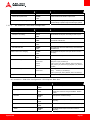
ADLINK Technology COM Express Express-HLE User manual
- Category
- Motherboards
- Type
- User manual

Express-HLE
User’s Manual
Manual Revision: 1.01
Revision Date: October 22, 2014
Part Number: 50-1J050-1010

Page 2 Express-HLE
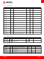
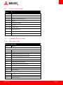
Revision History
Revision Description Date By
1.00 Initial release 2014-04-23 JC
1.01 Add BIOS beep codes; correct PCIe Configuration Switch settings 2014-10-22 JC

Express-HLE Page 3
Preface
Copyright 2014 ADLINK Technology, Inc.
This document contains proprietary information protected by copyright. All rights are reserved. No part of this manual may be reproduced by
any mechanical, electronic, or other means in any form without prior written permission of the manufacturer.
Disclaimer
The information in this document is subject to change without prior notice in order to improve reliability, design, and function and does not
represent a commitment on the part of the manufacturer. In no event will the manufacturer be liable for direct, indirect, special, incidental, or
consequential damages arising out of the use or inability to use the product or documentation, even if advised of the possibility of such
damages.
Environmental Responsibility
ADLINK is committed to fulfill its social responsibility to global environmental preservation through compliance with the European Union's
Restriction of Hazardous Substances (RoHS) directive and Waste Electrical and Electronic Equipment (WEEE) directive. Environmental
protection is a top priority for ADLINK. We have enforced measures to ensure that our products, manufacturing processes, components, and
raw materials have as little impact on the environment as possible. When products are at their end of life, our customers are encouraged to
dispose of them in accordance with the product disposal and/or recovery programs prescribed by their nation or company.
Trademarks
Product names mentioned herein are used for identification purposes only and may be trademarks and/or registered trademarks of their
respective companies.

Page 4 Express-HLE
Table of Contents
Revision History ............................................................................................................ 2
Preface............................................................................................................................ 3
1 Introduction ............................................................................................................ 6
2 Specifications.......................................................................................................... 7
2.1 Core System ..................................................................................................................................7
2.2 Expansion Busses ..........................................................................................................................7
2.3 Video .............................................................................................................................................7
2.4 Audio.............................................................................................................................................8
2.5 LAN................................................................................................................................................8
2.6 Multi I/O and Storage ...................................................................................................................8
2.7 TPM (Trusted Platform Module)...................................................................................................8
2.8 SEMA Board Controller .................................................................................................................8
2.9 Debug............................................................................................................................................8
2.10 Power Specifications .................................................................................................................9
2.11 Operating Temperatures...........................................................................................................9
2.12 Environmental ...........................................................................................................................9
2.13 Specification Compliance ..........................................................................................................9
2.14 Operating Systems ....................................................................................................................9
2.15 Function Diagram ................................................................................................................... 10
2.16 Mechanical Drawing............................................................................................................... 11
3 Pinouts and Signal Descriptions......................................................................... 12
3.1 AB / CD Pin Definitions............................................................................................................... 12
3.2 Signal Description Terminology ................................................................................................. 15
3.3 AB Signal Descriptions ............................................................................................................... 16
3.4 CD Signal Descriptions ............................................................................................................... 25
4 Connector Pinouts on Module............................................................................ 31
4.1 40-pin Debug Connector............................................................................................................ 32
4.2 Status LEDs................................................................................................................................. 34
4.3 XDP Debug header ..................................................................................................................... 35
4.4 Fan Connector............................................................................................................................ 36
4.5 BIOS Setup Defaults RESET Button ............................................................................................ 36
4.6 Express-HLE Switch Settings ...................................................................................................... 37
4.7 PCIe x16-to-two-x8 Adapter Card .............................................................................................. 39

Express-HLE Page 5
5 Smart Embedded Management Agent (SEMA) ................................................ 40
5.1 Board Specific SEMA Functions ................................................................................................. 41
6 System Resources................................................................................................. 43
6.1 System Memory Map................................................................................................................. 43
6.2 Direct Memory Access Channels ............................................................................................... 43
6.3 I/O Map...................................................................................................................................... 44
6.4 Interrupt Request (IRQ) Lines .................................................................................................... 46
6.5 PCI Configuration Space Map .................................................................................................... 48
6.6 PCI Interrupt Routing Map......................................................................................................... 49
6.7 SMBus Slave Addresses.............................................................................................................. 49
7 BIOS Setup ............................................................................................................ 50
7.1 Menu Structure.......................................................................................................................... 50
7.2 Main ........................................................................................................................................... 51
7.3 Advanced ................................................................................................................................... 56
7.4 Boot............................................................................................................................................ 72
7.5 Security ...................................................................................................................................... 73
7.6 Save & Exit ................................................................................................................................. 73
8 BIOS Checkpoints, Beep Codes ........................................................................... 74
8.1 Status Code Ranges.................................................................................................................... 75
8.2 Standard Status Codes ............................................................................................................... 75
8.3 OEM-Reserved Checkpoint Ranges............................................................................................ 81
9 Mechanical Information ...................................................................................... 82
9.1 Board-to-Board Connectors....................................................................................................... 82
9.2 Thermal Solution........................................................................................................................ 83
9.3 Mounting Methods .................................................................................................................... 85
9.4 Standoff Types ........................................................................................................................... 86
Safety Instructions ...................................................................................................... 87
Getting Service ............................................................................................................ 88

Page 6 Express-HLE
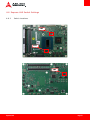
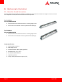
1 Introduction
The Express-HLE is a COM Express® COM.0 R2.1 Type 6 module supporting the 64-bit 4th Generation Intel® Core™ i7/i5/3 processor with
Intel® QM87 Chipset and 4th Generation Intel® Celeron® processor with Intel® HM86 Chipset. The Express-HLE is specifically designed for
customers who need high-level processing and graphics performance in a long product life solution.
The Express-HLE supports Intel® Hyper-Threading Technology (up to 4 cores, 8 threads) and ECC type DDR3L dual-channel memory at
1333/1600 MHz to provide excellent overall performance. Intel® Flexible Display Interface and Direct Media Interface provide high speed
connectivity from the CPU to the Intel® QM87/HM86 Chipset.
Integrated Intel Generation 7.5 Graphics includes features such as OpenGL 3.1, DirectX 11, Intel® Clear Video HD Technology, Advanced
Scheduler 2.0, 1.0, XPDM support, and DirectX Video Acceleration (DXVA) support for full AVC/VC1/MPEG2 hardware decode. Graphics
outputs include VGA, LVDS and three DDI ports supporting HDMI / DVI / DisplayPort. The Express-HLE is specifically designed for
customers with high-performance processing graphics requirements who want to outsource the custom core logic of their systems for
reduced development time.
The Express-HLE has dual stacked SODIMM sockets for up to 16 GB ECC type DDR3L memory. The Intel® Mobile QM87/HM86 Chipset
integrates VGA and dual-channel 18/24-bit LVDS display output. In addition to the onboard integrated graphics, a multiplexed PCI Express®
x16 Graphics bus is available for discrete graphics expansion or general purpose x8 or x4 PCI Express® connectivity.
The Express-HLE features a single onboard Gigabit Ethernet port, USB 3.0 ports and USB 2.0 ports, and SATA 6 Gb/s ports. Support is
provided for SMBus and I
2
C. The module is equipped with SPI AMI EFI BIOS with CMOS backup, supporting embedded features such as
remote console, CMOS backup, hardware monitor, and watchdog timer.

Express-HLE Page 7
2 Specifications
2.1 Core System
¾ CPU: 4th Generation Intel® Core™ and Celeron® Processors - 22nm, (formerly known as "Haswell Platform")
• Intel® Core™ i7-4860EQ 2.4 GHz (3.2 GHz Turbo), 47W (4C/GT3)
• Intel® Core™ i7-4700EQ 2.4/1.7 GHz (3.4 GHz Turbo), 47/37W (4C/GT2)
• Intel® Core™ i5-4400E 2.7 GHz (3.3 GHz Turbo), 37W (2C/GT2)
• Intel® Core™ i5-4402E 1.6 GHz (2.7 GHz Turbo), 25W (2C/GT2)
• Intel® Core™ i3-4100E 2.4 GHz (no Turbo) 3MB, 37W (2C/GT2)
• Intel® Core™ i5-4102E 1.6 GHz (no Turbo) 3MB, 25W (2C/GT2)
• Intel® Celeron 2000E 2.2 GHz (no Turbo) 35W (2C/GT1)
• Intel® Celeron 2002E 1.5 GHz (no Turbo) 25W (2C/GT1)
¾ L3 Cache: 6MB for i7-4650U, 3MB for i5-4400E, i5-4402E, i3-4100E and i3-4102E, 2MB for 2000E and 2002E
¾ Memory: Dual channel ECC 1600/1333 MHz DDR3L memory up to 16GB in dual SODIMM socket
¾ Chipset: Mobile Intel®
QM87 Chipset (Intel® Core™ i7/i5/i3)
Mobile Intel®
HM86 Chipset (Intel® Celeron)
¾ BIOS:
AMI EFI with CMOS backup in 8MB SPI BIOS with Intel® AMT 9.0 support (Intel® AMT not supported by HM86)
2.2 Expansion Busses
¾ PCI Express x16 (Gen3) or PCI Express (2 x8 or 1 x8 with 2 x4)
¾ 6 PCI Express x1 (AB): Lanes 0/1/2/3/4/5
¾ 1 PCI Express x1 (CD): Lane 6
¾ LPC bus, SMBus (system) , I
2
C (user)
2.3 Video
¾ Integrated in Processor: Intel® Generation 7.5 graphics core architecture
¾ GPU Feature Support:
• 3 independent and simultaneous display combinations of DisplayPort / HDMI / LVDS monitors
• Encode/transcode HD content
• Playback of high definition content including Blu-ray Disc*
• Superior image quality with sharper, more colorful images
• Playback of Blu-ray* disc S3D content using HDMI (1.4a spec compliant with 3D)
• DirectX* Video Acceleration (DXVA) support for accelerating video processing
• Full AVC/VC1/MPEG2 HW Decode
• Advanced Scheduler 2.0, 1.0, XPDM support
• Windows* 8, Windows* 7, OSX, Linux* OS support
• DirectX 11, DirectX
¾ Multi Display Support: 3 independent displays
¾ Display Types
• VGA Interface support with 300 MHz DAC Analog monitor support up to QXGA (2048 x 1536)
• LVDS Interface single/dual channel 18/24-bit LVDS through eDP (two lane) to LVDS Realtek RTD2136R
• Digital Display Ports x3
DDI1 supporting DisplayPort / HDMI / DVI
DDI2 supporting DisplayPort / HDMI / DVI
DDI3 supporting DisplayPort / HDMI / DVI

Page 8 Express-HLE
2.4 Audio
¾ Integrated: Intel® HD Audio integrated in PCH QM87/QM86
¾ Audio Codec: Realtek ALC886 on Express-BASE6
2.5 LAN
¾ Integrated: LAN MAC integrated in PCH QM87/HM86
¾ Intel PHY: Intel® Ethernet Controller i217LM
¾ Interface: 10/100/1000 GbE connection
2.6 Multi I/O and Storage
¾ Integrated in Intel® QM87/HM86 Chipset
¾ USB ports: 4 ports USB 3.0 (USB0,1 ,2 ,3) and 4 ports USB 2.0 (USB4, 5, 6, 7) – QM87
2 ports USB 3.0 (USB0, 1) and 6 ports USB 2.0 (USB3, 4, 5, 6, 7) – HM86
¾ SATA ports: 4 ports SATA 6Gb/s (SATA0, 1, 2, 3) – QM87
2 ports SATA 6Gb/s (SATA0, 1) and 2 ports SATA 3Gb/s (SATA2, 3) – HM86
¾ Serial: 2 UART ports COM1/2 with console redirection
¾ GPIO: 4 GPO and 4 GPI with interrupt
2.7 TPM (Trusted Platform Module)
¾ Chipset: ATMELAT97SC3204
¾ Type: TPM 1.2
2.8 SEMA Board Controller
¾ Type: ADLINK Smart Embedded Management Agent (SEMA)
¾ Supports:
• Voltage/Current monitoring
• Power sequence debug support
• AT/ATX mode control
• Logistics and Forensic information
• Flat Panel Control
• General Purpose I2C
• Failsafe BIOS (dual BIOS )
• Watchdog Timer and Fan Control
2.9 Debug
¾ 40-pin flat cable connector to be used with DB-40 debug module
• supports: BIOS POSTCODE LED, BMC access, SPI BIOS flashing, Power Testpoints, Debug LEDs
¾ 60-pin XDP header for ICE debug of CPU/Chipset

Express-HLE Page 9
2.10 Power Specifications
¾ Power Modes: AT and ATX mode (AT mode start controlled by SEMA)
¾ Standard Voltage Input: ATX = 12V±5% / 5Vsb ±5% or AT = 12V ±5%
¾ Wide Voltage Input: ATX = 8.5~20 V / 5Vsb ±5% or AT = 8.5 ~20V
¾ Power Management: ACPI 4.0 compliant, Smart Battery support
¾ Power States: supports C1-C6, S0, S1, S4, S3, S5, S5 ECO mode (Wake on USB S3/S4, WOL S3/S4/S5)
2.11 Operating Temperatures
¾ Standard Operating Temperature: 0°C to 60°C (wide voltage input)
¾ Extreme Rugged Operating Temperature: -40°C to 85°C (standard voltage input)
2.12 Environmental
¾ Humidity: 5-90% RH operating, non-condensing
5-95% RH storage (and operating with conformal coating).
¾ Shock and Vibration: IEC 60068-2-64 and IEC-60068-2-27
MIL-STD-202F, Method 213B, Table 213-I, Condition A and Method 214A, Table 214-I, Condition D
¾ Halt: Thermal Stress, Vibration Stress, Thermal Shock and Combined Test
2.13 Specification Compliance
¾ PICMG COM.0: Rev 2.1 Type 6, basic size 125 x 95
2.14 Operating Systems
¾ Standard Support: Windows 7/8 32/64-bit, Linux 32/64-bit
¾ Extended Support (BSP): WEC7/8, Linux , VxWorks

Page 10 Express-HLE
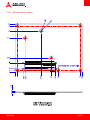
2.15 Function Diagram
“Haswell”
ATMEL
AT97SC3204
NCT5104D
Mobile Intel®
QM87/HM86
Chipset
i217LM
PCA9535
SMBus
4x GP0
GP I
2
C
LPC bus
1333/1600 MHz
1~8 GB DDR3L
PCI Express x16 (Gen3)
2 x8 or 1 x8 + 2 x4
SPI
4x GPI
Debug
header
60-pin
VGA
PCIe x1
(port 7)
HD Audio
UART1
UART0
DDC I
2
C
1333/1600 MHz
1~8 GB DDR3L
SPI_CS0
SPI_CS1
SPI_CS#
D
D
I
1
(
p
o
r
t
B
)
D
P
/ H
D
M
I / D
V
I
/ S
D
V
O
DDI 2 (port C)
DP / HDMI / DVI
DDI 3 (port D)
DP / HDMI / DVI
-40+85°C
RTD2136R
eDP
2 lane
6x PCIe x1 (Gen2)
(port 0~5)
8x USB 1.1/2.0
4x USB 3.0 upgrade (QM87)
2x USB 3.0 upgrade (HM86)
1x PCIe x1 (Gen2)
(port 6)
4x SATA3 (QM87)
2x SATA3 & 2x SATA2 (HM86)
single / dual
18/24-bit LVDS

Express-HLE Page 11
2.16 Mechanical Drawing

Page 12 Express-HLE
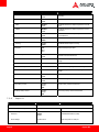
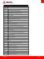
3 Pinouts and Signal Descriptions
3.1 AB / CD Pin Definitions
The Express-HLE is a Type 6 module supporting USB3.0 and DDI channels on the CD connector
All pins in the COM Express specification are described, including those not supported on the Express-HLE. Those not supported on the
Express-HLE module are crossed out
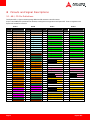
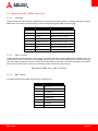
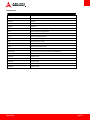
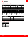
Row A Row B Row C Row D
Pin Name Pin Name Pin Name Pin Name
A1
GND (FIXED)
B1
GND (FIXED)
C1
GND FIXED)
D1
GND FIXED)
A2
GBE0_MDI3-
B2
GBE0_ACT#
C2
GND
D2
GND
A3
GBE0_MDI3+
B3
LPC_FRAME#
C3
USB_SSRX0-
D3
USB_SSTX0-
A4
GBE0_LINK100#
B4
LPC_AD0
C4
USB_SSRX0+
D4
USB_SSTX0+
A5
GBE0_LINK1000#
B5
LPC_AD1
C5
GND
D5
GND
A6
GBE0_MDI2-
B6
LPC_AD2
C6
USB_SSRX1-
D6
USB_SSTX1-
A7
GBE0_MDI2+
B7
LPC_AD3
C7
USB_SSRX1+
D7
USB_SSTX1+
A8
GBE0_LINK#
B8
LPC_DRQ0#
C8
GND
D8
GND
A9
GBE0_MDI1-
B9
LPC_DRQ1#
C9
USB_SSRX2- *
D9
USB_SSTX2- *
A10
GBE0_MDI1+
B10
LPC_CLK
C10
USB_SSRX2+ *
D10
USB_SSTX2+ *
A11
GND (FIXED)
B11
GND (FIXED)
C11
GND (FIXED)
D11
GND (FIXED)
A12
GBE0_MDI0-
B12
PWRBTN#
C12
USB_SSRX3- *
D12
USB_SSTX3- *
A13
GBE0_MDI0+
B13
SMB_CK
C13
USB_SSRX3+ *
D13
USB_SSTX3+ *
A14
GBE0_CTREF
B14
SMB_DAT
C14
GND
D14
GND
A15
SUS_S3#
B15
SMB_ALERT#
C15
DDI1_PAIR6+
D15
DDI1_CTRLCLK_AUX+
A16
SATA0_TX+
B16
SATA1_TX+
C16
DDI1_PAIR6-
D16
DDI1_CTRLDATA_AUX
A17
SATA0_TX-
B17
SATA1_TX-
C17
RSVD
D17
RSVD
A18
SUS_S4#
B18
SUS_STAT#
C18
RSVD
D18
RSVD
A19
SATA0_RX+
B19
SATA1_RX+
C19
PCIE_RX6+
D19
PCIE_TX6+
A20
SATA0_RX-
B20
SATA1_RX-
C20
PCIE_RX6-
D20
PCIE_TX6-
A21
GND (FIXED)
B21
GND (FIXED)
C21
GND (FIXED)
D21
GND (FIXED)
A22
SATA2_TX+
B22
SATA3_TX+
C22
PCIE_RX7+
D22
PCIE_TX7+
A23
SATA2_TX-
B23
SATA3_TX-
C23
PCIE_RX7-
D23
PCIE_TX7-
A24
SUS_S5#
B24
PWR_OK
C24
DDI1_HPD
D24
RSVD
A25
SATA2_RX+
B25
SATA3_RX+
C25
DDI1_PAIR4+
D25
RSVD
A26
SATA2_RX-
B26
SATA3_RX-
C26
DDI1_PAIR4-
D26
DDI1_PAIR0+
A27
BATLOW#
B27
WDT
C27
RSVD
D27
DDI1_PAIR0-
A28
(S)ATA_ACT#
B28
AC/HDA_SDIN2
C28
RSVD
D28
RSVD
A29
AC/HDA_SYNC
B29
AC/HDA_SDIN1
C29
DDI1_PAIR5+
D29
DDI1_PAIR1+
A30
AC/HDA_RST#
B30
AC/HDA_SDIN0
C30
DDI1_PAIR5-
D30
DDI1_PAIR1-
A31
GND (FIXED)
B31
GND (FIXED)
C31
GND (FIXED)
D31
GND (FIXED)
A32
AC/HDA_BITCLK
B32
SPKR
C32
DDI2_CTRLCLK_AUX+
D32
DDI1_PAIR2+
A33
AC/HDA_SDOUT
B33
I2C_CK
C33
DDI2_CTRLDATA_AUX-
D33
DDI1_PAIR2-
A34
BIOS_DIS0#
B34
I2C_DAT
C34
DDI2_DDC_AUX_SEL
D34
DDI1_DDC_AUX_SEL
A35
THRMTRIP#
B35
THRM#
C35
RSVD
D35
RSVD

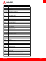
Express-HLE Page 13
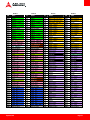
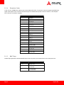
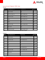
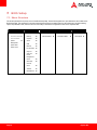
Row A Row B Row C Row D
Pin Name Pin Name Pin Name Pin Name
A36
USB6-
B36
USB7-
C36
DDI3_CTRLCLK_AUX+
D36
DDI1_PAIR3+
A37
USB6+
B37
USB7+
C37
DDI3_CTRLDATA_AUX-
D37
DDI1_PAIR3-
A38
USB_6_7_OC#
B38
USB_4_5_OC#
C38
DDI3_DDC_AUX_SEL
D38
RSVD
A39
USB4-
B39
USB5-
C39
DDI3_PAIR0+
D39
DDI2_PAIR0+
A40
USB4+
B40
USB5+
C40
DDI3_PAIR0-
D40
DDI2_PAIR0-
A41
GND (FIXED)
B41
GND (FIXED)
C41
GND (FIXED)
D41
GND (FIXED)
A42
USB2-
B42
USB3-
C42
DDI3_PAIR1+
D42
DDI2_PAIR1+
A43
USB2+
B43
USB3+
C43
DDI3_PAIR1-
D43
DDI2_PAIR1-
A44
USB_2_3_OC#
B44
USB_0_1_OC#
C44
DDI3_HPD
D44
DDI2_HPD
A45
USB0-
B45
USB1-
C45
RSVD
D45
RSVD
A46
USB0+
B46
USB1+
C46
DDI3_PAIR2+
D46
DDI2_PAIR2+
A47
VCC_RTC
B47
EXCD1_PERST#
C47
DDI3_PAIR2-
D47
DDI2_PAIR2-
A48
EXCD0_PERST#
B48
EXCD1_CPPE#
C48
RSVD
D48
RSVD
A49
EXCD0_CPPE#
B49
SYS_RESET#
C49
DDI3_PAIR3+
D49
DDI2_PAIR3+
A50
LPC_SERIRQ
B50
CB_RESET#
C50
DDI3_PAIR3-
D50
DDI2_PAIR3-
A51
GND (FIXED)
B51
GND (FIXED)
C51
GND (FIXED)
D51
GND (FIXED)
A52
PCIE_TX5+
B52
PCIE_RX5+
C52
PEG_RX0+
D52
PEG_TX0+
A53
PCIE_TX5-
B53
PCIE_RX5-
C53
PEG_RX0-
D53
PEG_TX0-
A54
GPI0
B54
GPO1
C54
TYPE0#
D54
PEG_LANE_RV#
A55
PCIE_TX4+
B55
PCIE_RX4+
C55
PEG_RX1+
D55
PEG_TX1+
A56
PCIE_TX4-
B56
PCIE_RX4-
C56
PEG_RX1-
D56
PEG_TX1-
A57
GND
B57
GPO2
C57
TYPE1#
D57
TYPE2#
A58
PCIE_TX3+
B58
PCIE_RX3+
C58
PEG_RX2+
D58
PEG_TX2+
A59
PCIE_TX3-
B59
PCIE_RX3-
C59
PEG_RX2-
D59
PEG_TX2-
A60
GND (FIXED)
B60
GND (FIXED)
C60
GND (FIXED)
D60
GND (FIXED)
A61
PCIE_TX2+
B61
PCIE_RX2+
C61
PEG_RX3+
D61
PEG_TX3+
A62
PCIE_TX2-
B62
PCIE_RX2-
C62
PEG_RX3-
D62
PEG_TX3-
A63
GPI1
B63
GPO3
C63
RSVD
D63
RSVD
A64
PCIE_TX1+
B64
PCIE_RX1+
C64
RSVD
D64
RSVD
A65
PCIE_TX1-
B65
PCIE_RX1-
C65
PEG_RX4+
D65
PEG_TX4+
A66
GND
B66
WAKE0#
C66
PEG_RX4-
D66
PEG_TX4-
A67
GPI2
B67
WAKE1#
C67
RSVD
D67
GND
A68
PCIE_TX0+
B68
PCIE_RX0+
C68
PEG_RX5+
D68
PEG_TX5+
A69
PCIE_TX0-
B69
PCIE_RX0-
C69
PEG_RX5-
D69
PEG_TX5-
A70
GND (FIXED)
B70
GND (FIXED)
C70
GND (FIXED)
D70
GND (FIXED)
A71
LVDS_A0+
B71
LVDS_B0+
C71
PEG_RX6+
D71
PEG_TX6+
A72
LVDS_A0-
B72
LVDS_B0-
C72
PEG_RX6-
D72
PEG_TX6-
A73
LVDS_A1+
B73
LVDS_B1+
C73
GND
D73
GND
A74
LVDS_A1-
B74
LVDS_B1-
C74
PEG_RX7+
D74
PEG_TX7+
A75
LVDS_A2+
B75
LVDS_B2+
C75
PEG_RX7-
D75
PEG_TX7-
A76
LVDS_A2-
B76
LVDS_B2-
C76
GND
D76
GND
A77
LVDS_VDD_EN
B77
LVDS_B3+
C77
RSVD
D77
RSVD
A78
LVDS_A3+
B78
LVDS_B3-
C78
PEG_RX8+
D78
PEG_TX8+
A79
LVDS_A3-
B79
LVDS_BKLT_EN
C79
PEG_RX8-
D79
PEG_TX8-
A80
GND (FIXED)
B80
GND (FIXED)
C80
GND (FIXED)
D80
GND (FIXED)

Page 14 Express-HLE
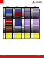
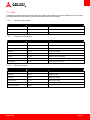
Row A Row B Row C Row D
Pin Name Pin Name Pin Name Pin Name
A81
LVDS_A_CK+
B81
LVDS_B_CK+
C81
PEG_RX9+
D81
PEG_TX9+
A82
LVDS_A_CK-
B82
LVDS_B_CK-
C82
PEG_RX9-
D82
PEG_TX9-
A83
LVDS_I2C_CK
B83
LVDS_BKLT_CTRL
C83
TPM_PP
D83
RSVD
A84
LVDS_I2C_DAT
B84
VCC_5V_SBY
C84
GND
D84
GND
A85
GPI3
B85
VCC_5V_SBY
C85
PEG_RX10+
D85
PEG_TX10+
A86
RSVD
B86
VCC_5V_SBY
C86
PEG_RX10-
D86
PEG_TX10-
A87
RSVD
B87
VCC_5V_SBY
C87
GND
D87
GND
A88
PCIE0_CK_REF+
B88
BIOS_DIS1#
C88
PEG_RX11+
D88
PEG_TX11+
A89
PCIE0_CK_REF-
B89
VGA_RED
C89
PEG_RX11-
D89
PEG_TX11-
A90
GND (FIXED)
B90
GND (FIXED)
C90
GND (FIXED)
D90
GND (FIXED)
A91
SPI_POWER
B91
VGA_GRN
C91
PEG_RX12+
D91
PEG_TX12+
A92
SPI_MISO
B92
VGA_BLU
C92
PEG_RX12-
D92
PEG_TX12-
A93
GPO0
B93
VGA_HSYNC
C93
GND
D93
GND
A94
SPI_CLK
B94
VGA_VSYNC
C94
PEG_RX13+
D94
PEG_TX13+
A95
SPI_MOSI
B95
VGA_I2C_CK
C95
PEG_RX13-
D95
PEG_TX13-
A96
TPM_PP
B96
VGA_I2C_DAT
C96
GND
D96
GND
A97
TYPE10#
B97
SPI_CS#
C97
RSVD
D97
RSVD
A98
SER0_TX
B98
RSVD
C98
PEG_RX14+
D98
PEG_TX14+
A99
SER0_RX
B99
RSVD
C99
PEG_RX14-
D99
PEG_TX14-
A100
GND (FIXED)
B100
GND (FIXED)
C100
GND (FIXED)
D100
GND (FIXED)
A101
SER1_TX
B101
FAN_PWMOUT
C101
PEG_RX15+
D101
PEG_TX15+
A102
SER1_RX
B102
FAN_TACHIN
C102
PEG_RX15-
D102
PEG_TX15-
A103
LID#
B103
SLEEP#
C103
GND
D103
GND
A104
VCC_12V
B104
VCC_12V
C104
VCC_12V
D104
VCC_12V
A105
VCC_12V
B105
VCC_12V
C105
VCC_12V
D105
VCC_12V
A106
VCC_12V
B106
VCC_12V
C106
VCC_12V
D106
VCC_12V
A107
VCC_12V
B107
VCC_12V
C107
VCC_12V
D107
VCC_12V
A108
VCC_12V
B108
VCC_12V
C108
VCC_12V
D108
VCC_12V
A109
VCC_12V
B109
VCC_12V
C109
VCC_12V
D109
VCC_12V
A110
GND (FIXED)
B110
GND (FIXED)
C110
GND (FIXED)
D110
GND (FIXED)
*Note: USB 3.0 upgrade signals for ports 2, 3 are supported by QM87 only.

Express-HLE Page 15
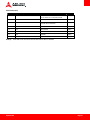
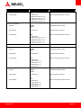
3.2 Signal Description Terminology
The following terms are used in the COM Express AB/CD Signal Descriptions below.
I Input to the Module
O Output from the Module
I/O Bi-directional input / output signal
OD Open drain output
I 3.3V Input 3.3V tolerant
I 5V Input 5V tolerant
O 3.3V Output 3.3V signal level
O 5V Output 5V signal level
I/O 3.3V Bi-directional signal 3.3V tolerant
I/O 5V Bi-directional signal 5V tolerant
I/O 3.3Vsb Input 3.3V tolerant active in standby state
P Power Input/Output
REF Reference voltage output that may be sourced from a module power plane.
PDS Pull-down strap. This is an output pin on the module that is either tied to GND or not connected.
The signal is used to indicate the PICMG module type to the Carrier Board.
PU ADLINK implemented pull-up resistor on module
PD ADLINK implemented pull-down resistor on module

Page 16 Express-HLE
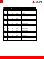
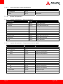
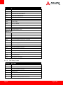
3.3 AB Signal Descriptions
3.3.1 Audio Signals
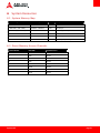
Signal Pin # Description I/O PU/PD Comment
AC_RST# /
HDA_RST#
A30 Reset output to codec, active low. O 3.3VSB VSB because PCH uses suspend
power for RESET
AC_SYNC /
HDA_SYNC
A29 Sample-synchronization signal to the codec(s). O 3.3V
AC_BITCLK /
HDA_BITCLK
A32 Serial data clock generated by the external
codec(s).
I/O 3.3V
AC _SDOUT /
HDA_SDOUT
A33 Serial TDM data output to the codec. O 3.3V
AC _SDIN[2:0]
HDA_SDIN[2:0]
B28
B30
Serial TDM data inputs from up to 3 codecs. I/O 3.3V
3.3.2 Analog VGA
Signal Pin # Description I/O PU/PD Comment
VGA_RED B89 Red for monitor.
Analog DAC output, designed to drive a
37.5-Ohm equivalent load.
O Analog
PD 150R
Shall also be terminated on the
carrier with 150Ω resistor to
ground close to VGA connector
VGA_GRN B91 Green for monitor
Analog DAC output, designed to drive a
37.5-Ohm equivalent load.
O Analog
PD 150R
Shall also be terminated on the
carrier with 150Ω resistor to
ground close to VGA connector
VGA_BLU B92 Blue for monitor.
Analog DAC output, designed to drive a
37.5-Ohm equivalent load.
O Analog
PD 150R
Shall also be terminated on the
carrier with 150Ω resistor to
ground close to VGA connector
VGA_HSYNC B93 Horizontal sync output to VGA monitor O 3.3V
VGA_VSYNC B94 Vertical sync output to VGA monitor O 3.3V
VGA_I2C_CK B95 DDC clock line (I²C port dedicated to identify
VGA monitor capabilities)
I/O OD 3.3V PU 2k2 3.3V
VGA_I2C_DAT B96 DDC data line. I/O OD 3.3V PU 2k2 3.3V

Express-HLE Page 17
3.3.3 LVDS
Signal Pin # Description I/O PU/PD Comment
LVDS_A0+
LVDS_A0-
LVDS_A1+
LVDS_A1-
LVDS_A2+
LVDS_A2-
LVDS_A3+
LVDS_A3-
A71
A72
A73
A74
A75
A76
A78
A79
LVDS Channel A differential pairs O LVDS
LVDS_A_CK+
LVDS_A_CK-
A81
A82
LVDS Channel A differential clock O LVDS
LVDS_B0+
LVDS_B0-
LVDS_B1+
LVDS_B1-
LVDS_B2+
LVDS_B2-
LVDS_B3+
LVDS_B3-
B71
B72
B73
B74
B75
B76
B77
B78
LVDS Channel B differential pairs O LVDS
LVDS_B_CK+
LVDS_B_CK-
B81
B82
LVDS Channel B differential clock O LVDS
LVDS_VDD_EN A77 LVDS panel power enable O 3.3V
LVDS_BKLT_EN B79 LVDS panel backlight enable O 3.3V
LVDS_BKLT_CTRL B83 LVDS panel backlight brightness control O 3.3V PD 100K
Realtek ePD to LVDS
requirement
LVDS_I2C_CK A83 DDC lines used for flat panel detection and control. O 3.3V PU 2k2 3.3V
LVDS_I2C_DAT A84 DDC lines used for flat panel detection and control. I/O 3.3V PU 2k2 3.3V
3.3.4 Gigabit Ethernet
Gigabit Ethernet Pin # Description I/O PU/PD Comment
GBE0_MDI0+
GBE0_MDI0-
GBE0_MDI1+
GBE0_MDI1-
GBE0_MDI2+
GBE0_MDI2-
GBE0_MDI3+
GBE0_MDI3-
A13
A12
A10
A9
A7
A6
A3
A2
Gigabit Ethernet Controller 0: Media Dependent Interface Differential Pairs
0, 1, 2, 3. The MDI can operate in 1000, 100, and 10Mbit/sec modes.
Some pairs are unused in some modes according to the following:
1000BASE-T 100BASE-TX 10BASE-T
MDI[0]+/- B1_DA+/- TX+/- TX+/-
MDI[1]+/- B1_DB+/- RX+/- RX+/-
MDI[2]+/- B1_DC+/-
MDI[3]+/- B1_DD+/-
I/O Analog Twisted pair
signals for
external
transformer.
GBE0_ACT# B2 Gigabit Ethernet Controller 0 activity indicator, active low. O 3.3VSB PU 10k
3.3VSB
GBE0_LINK# A8 Gigabit Ethernet Controller 0 link indicator, active low. O 3.3VSB
GBE0_LINK100# A4 Gigabit Ethernet Controller 0 100Mbit/sec link indicator, active low. O 3.3VSB
GBE0_LINK1000# A5 Gigabit Ethernet Controller 0 1000Mbit/sec link indicator, active low. O 3.3VSB
GBE0_CTREF A14 Reference voltage for Carrier Board Ethernet channel 1 and 2 magnetics
center tap. The reference voltage is determined by the requirements of the
Module PHY and may be as low as 0V and as high as 3.3V. The reference
voltage output shall be current limited on the Module. In the case in which
the reference is shorted to ground, the current shall be 250 mA or less.
GND min
3.3V max

Page 18 Express-HLE
3.3.5 Serial ATA
Signal Pin # Description I/O PU/PD Comment
SATA0_TX+
SATA0_TX-
A16
A17
Serial ATA channel 0, Transmit Output
differential pair.
O SATA AC coupled on Module
SATA0_RX+
SATA0_RX-
A19
A20
Serial ATA channel 0, Receive Input
differential pair.
I SATA AC coupled on Module
SATA1_TX+
SATA1_TX-
B16
B17
Serial ATA channel 1, Transmit Output
differential pair.
O SATA AC coupled on Module
SATA1_RX+
SATA1_RX-
B19
B20
Serial ATA channel 1, Receive Input
differential pair.
I SATA AC coupled on Module
SATA2_TX+
SATA2_TX-
A22
A23
Serial ATA channel 2, Transmit Output
differential pair.
O SATA AC coupled on Module
SATA2_RX+
SATA2_RX-
A25
A26
Serial ATA channel 2, Receive Input
differential pair.
I SATA AC coupled on Module
SATA3_TX+
SATA3_TX-
B22
B23
Serial ATA channel 3, Transmit Output
differential pair.
O SATA AC coupled on Module
SATA3_RX+
SATA3_RX-
B25
B26
Serial ATA channel 3, Receive Input
differential pair.
I SATA AC coupled on Module
(S)ATA_ACT# A28 ATA (parallel and serial) or SAS activity
indicator, active low.
O 3.3V

Express-HLE Page 19
3.3.6 PCI Express
Signal Pin # Description I/O PU/PD Comment
PCIE_TX0+
PCIE_TX0-
A68
A69
PCI Express channel 0, Transmit Output differential
pair.
O PCIE AC coupled on Module
PCIE_RX0+
PCIE_RX0-
B68
B69
PCI Express channel 0, Receive Input differential
pair.
I PCIE AC coupled off Module
PCIE_TX1+
PCIE_TX1-
A64
A65
PCI Express channel 1, Transmit Output differential
pair.
O PCIE AC coupled on Module
PCIE_RX1+
PCIE_RX1-
B64
B65
PCI Express channel 1, Receive Input differential
pair.
I PCIE AC coupled off Module
PCIE_TX2+
PCIE_TX2-
A61
A62
PCI Express channel 2, Transmit Output differential
pair.
O PCIE AC coupled on Module
PCIE_RX2+
PCIE_RX2-
B61
B62
PCI Express channel 2, Receive Input differential
pair.
I PCIE AC coupled off Module
PCIE_TX3+
PCIE_TX3-
A58
A59
PCI Express channel 3, Transmit Output differential
pair.
O PCIE AC coupled on Module
PCIE_RX3+
PCIE_RX3-
B58
B59
PCI Express channel 3, Receive Input differential
pair.
I PCIE AC coupled off Module
PCIE_TX4+
PCIE_TX4-
A55
A56
PCI Express channel 4, Transmit Output differential
pair.
O PCIE AC coupled on Module
PCIE_RX4+
PCIE_RX4-
B55
B56
PCI Express channel 4, Receive Input differential
pair.
I PCIE AC coupled off Module
PCIE_TX5+
PCIE_TX5-
A52
A53
PCI Express channel 5, Transmit Output differential
pair.
O PCIE AC coupled on Module
PCIE_RX5+
PCIE_RX5-
B52
B53
PCI Express channel 5, Receive Input differential
pair.
I PCIE AC coupled off Module
PCIE_CLK_REF+
PCIE_CLK_REF-
A88
A89
PCI Express Reference Clock output for all PCI
Express and PCI Express Graphics Lanes.
O PCIE
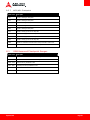
3.3.7 Express Card
Signal Pin # Description I/O PU/PD Comment
EXCD0_CPPE#
EXCD1_CPPE#
A49
B48
PCI ExpressCard: PCI Express capable card request I 3.3V PU 10k 3.3V
EXCD0_PERST#
EXCD1_PERST#
A48
B47
PCI ExpressCard: reset O 3.3V
3.3.8 LPC Bus
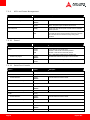
Signal Pin # Description I/O PU/PD Comment
LPC_AD[0:3] B4-B7 LPC multiplexed address, command and data bus I/O 3.3V
LPC_FRAME# B3 LPC frame indicates the start of an LPC cycle O 3.3V
LPC_DRQ0#
LPC_DRQ1#
B8
B9
LPC serial DMA request I 3.3V
LPC_SERIRQ A50 LPC serial interrupt I/O OD 3.3V PU 8k2 3.3V
LPC_CLK B10 LPC clock output - 33MHz nominal O 3.3V

Page 20 Express-HLE
3.3.9 USB
Signal Pin # Description I/O PU/PD Comment
USB0+
USB0-
A46
A45
USB differential data pairs for Port 0 I/O 3.3VSB USB 1.1/ 2.0 compliant
USB1+
USB1-
B46
B45
USB differential data pairs for Port 1 I/O 3.3VSB USB 1.1/ 2.0 compliant
USB2+
USB2-
A43
A42
USB differential data pairs for Port 1 I/O 3.3VSB USB 1.1/ 2.0 compliant
USB3+
USB3-
B43
B42
USB differential data pairs for Port 2 I/O 3.3VSB USB 1.1/ 2.0 compliant
USB4+
USB4-
A40
A39
USB differential data pairs for Port 3 I/O 3.3VSB USB 1.1/ 2.0 compliant
USB5+
USB5-
B40
B39
USB differential data pairs for Port 4 I/O 3.3VSB USB 1.1/ 2.0 compliant
USB6+
USB6-
A37
A36
USB differential data pairs for Port 5 I/O 3.3VSB USB 1.1/ 2.0 compliant
USB7+
USB7-
B37
B37
USB differential data pairs for Port 6 I/O 3.3VSB USB 1.1/ 2.0 compliant
USB_0_1_OC# B44 USB over-current sense, USB ports 0 and 1. A pull-up
for this line shall be present on the module. An open
drain driver from a USB current monitor on the carrier
board may drive this line low.
I 3.3VSB PU 10k 3.3VSB Do not pull high on carrier
USB_2_3_OC# A44 USB over-current sense, USB ports 2 and 3. A pull-up
for this line shall be present on the module. An open
drain driver from a USB current monitor on the carrier
board may drive this line low. .
I 3.3VSB PU 10k 3.3VSB Do not pull high on carrier
USB_4_5_OC# B38 USB over-current sense, USB ports 4 and 5. A pull-up
for this line shall be present on the module. An open
drain driver from a USB current monitor on the carrier
board may drive this line low.
I 3.3VSB PU 10k 3.3VSB Do not pull high on carrier
USB_6_7_OC# A38 USB over-current sense, USB ports 6 and 7. A pull-up
for this line shall be present on the module. An open
drain driver from a USB current monitor on the carrier
board may drive this line low.
I 3.3VSB PU 10k 3.3VSB Do not pull high on carrier
Page is loading ...
Page is loading ...
Page is loading ...
Page is loading ...
Page is loading ...
Page is loading ...
Page is loading ...
Page is loading ...
Page is loading ...
Page is loading ...
Page is loading ...
Page is loading ...
Page is loading ...
Page is loading ...
Page is loading ...
Page is loading ...
Page is loading ...
Page is loading ...
Page is loading ...
Page is loading ...
Page is loading ...
Page is loading ...
Page is loading ...
Page is loading ...
Page is loading ...
Page is loading ...
Page is loading ...
Page is loading ...
Page is loading ...
Page is loading ...
Page is loading ...
Page is loading ...
Page is loading ...
Page is loading ...
Page is loading ...
Page is loading ...
Page is loading ...
Page is loading ...
Page is loading ...
Page is loading ...
Page is loading ...
Page is loading ...
Page is loading ...
Page is loading ...
Page is loading ...
Page is loading ...
Page is loading ...
Page is loading ...
Page is loading ...
Page is loading ...
Page is loading ...
Page is loading ...
Page is loading ...
Page is loading ...
Page is loading ...
Page is loading ...
Page is loading ...
Page is loading ...
Page is loading ...
Page is loading ...
Page is loading ...
Page is loading ...
Page is loading ...
Page is loading ...
Page is loading ...
Page is loading ...
Page is loading ...
Page is loading ...
Page is loading ...
-
 1
1
-
 2
2
-
 3
3
-
 4
4
-
 5
5
-
 6
6
-
 7
7
-
 8
8
-
 9
9
-
 10
10
-
 11
11
-
 12
12
-
 13
13
-
 14
14
-
 15
15
-
 16
16
-
 17
17
-
 18
18
-
 19
19
-
 20
20
-
 21
21
-
 22
22
-
 23
23
-
 24
24
-
 25
25
-
 26
26
-
 27
27
-
 28
28
-
 29
29
-
 30
30
-
 31
31
-
 32
32
-
 33
33
-
 34
34
-
 35
35
-
 36
36
-
 37
37
-
 38
38
-
 39
39
-
 40
40
-
 41
41
-
 42
42
-
 43
43
-
 44
44
-
 45
45
-
 46
46
-
 47
47
-
 48
48
-
 49
49
-
 50
50
-
 51
51
-
 52
52
-
 53
53
-
 54
54
-
 55
55
-
 56
56
-
 57
57
-
 58
58
-
 59
59
-
 60
60
-
 61
61
-
 62
62
-
 63
63
-
 64
64
-
 65
65
-
 66
66
-
 67
67
-
 68
68
-
 69
69
-
 70
70
-
 71
71
-
 72
72
-
 73
73
-
 74
74
-
 75
75
-
 76
76
-
 77
77
-
 78
78
-
 79
79
-
 80
80
-
 81
81
-
 82
82
-
 83
83
-
 84
84
-
 85
85
-
 86
86
-
 87
87
-
 88
88
-
 89
89


ADLINK Technology COM Express Express-HLE User manual
- Category
- Motherboards
- Type
- User manual
Ask a question and I''ll find the answer in the document
Finding information in a document is now easier with AI
Related papers
-
ADLINK Technology cExpress-HL User manual
-
-
-
-
-
-
-
-
-
Other documents
-
Biostar H77MU3 User manual
-
DFI WL9A3 Preliminary Owner's manual
-
ROHS EmETXe-i9652 User manual
-
Aaeon COM-R2KC6 User manual
-
DFI HM960-QM87 Owner's manual
-
-
American Megatrends Debug Rx Quick start guide
-
-
-