Page is loading ...

CPV5000 CompactPCI
®
Single Board Computer
Installation and Reference
Guide
CPV5000A/IH3

Notice
While reasonable efforts have been made to assure the accuracy of this document,
Motorola, Inc. assumes no liability resulting from any omissions in this document, or from
the use of the information obtained therein. Motorola reserves the right to revise this
document and to make changes from time to time in the content hereof without obligation
of Motorola to notify any person of such revision or changes.
No part of this material may be reproduced or copied in any tangible medium, or stored in
a retrieval system, or transmitted in any form, or by any means, radio, electronic,
mechanical, photocopying, recording or facsimile, or otherwise, without the prior written
permission of Motorola, Inc.
It is possible that this publication may contain reference to, or information about Motorola
products (machines and programs), programming, or services that are not announced in
your country. Such references or information must not be construed to mean that Motorola
intends to announce such Motorola products, programming, or services in your country.
Restricted Rights Legend
If the documentation contained herein is supplied, directly or indirectly, to the U.S.
Government, the following notice shall apply unless otherwise agreed to in writing by
Motorola, Inc.
Use, duplication, or disclosure by the Government is subject to restrictions as set forth in
subparagraph (c)(1)(ii) of the Rights in Technical Data and Computer Software clause at
DFARS 252.227-7013.
Motorola, Inc.
Computer Group
2900 South Diablo Way
Tempe, Arizona 85282

Preface
The CPV5000 Single Board Computer Installation and Reference Guide describes the
installation, components, and configurations of the CPV5000. The document should be
used by anyone who wants general as well as technical information about the CPV5000
Single Board Computer.
Motorola
®
and the Motorola symbol are registered trademarks of Motorola, Inc.
Intel
®
and
Pentium
®
are registered trademarks of Intel Corporation.
AMD and K-6
®
are registered trademarks of Advanced Micro Devices, Inc.
Windows NT
®
and Windows 95
®
are registered trademarks of Microsoft Corporation.
CompactPCI
®
is a registered trademark of PCI Industrial Computer Manufacturers Group.
OS/2
®
is a registered trademark of International Business Machines Corporation.
IBM
®
is a registered trademark of International Business Machines Corporation.
NetWare
®
is a registered trademark of Novell, Inc. in the U.S. and other countries.
AMIBIOS is a trademark of American Megatrends, Inc.
SCO
®
and the SCO logo are trademarks or registered trademarks of The Santa Cruz
Corporation, Inc. in the U.S. and other countries.
UNIX
®
is a registered trademark of Open Group in the U.S. and other countries.
WATCHDOG is a trademark of National Semiconductor Corporation.
All other products mentioned in this document are trademarks or registered trademarks of
their respective holders.
The computer programs stored in the Read Only Memory of this device contain material
copyrighted by Motorola Inc., first published 1990, and may be used only under a license
such as the License for Computer Programs (Article 14) contained in Motorola’s Terms and
Conditions of Sale, Rev. 1/79.
All Motorola PWBs (printed wiring boards) are manufactured by UL-recognized
manufacturers, with a flammability rating of 94V-0.
© Copyright Motorola, Inc. 1998
All Rights Reserved
Printed in the United States of America
November 1998

Safety Summary
Safety Depends On You
The following general safety precautions must be observed during all phases of operation, service, and repair of this
equipment. Failure to comply with these precautions or with specific warnings elsewhere in this manual violates safety
standards of design, manufacture, and intended use of the equipment. Motorola, Inc. assumes no liability for the
customer’s failure to comply with these requirements.
The safety precautions listed below represent warnings of certain dangers of which Motorola is aware. You, as the
user of the product, should follow these warnings and all other safety precautions necessary for the safe operation of
the equipment in your operating environment.
Ground the Instrument.
To minimize shock hazard, the equipment chassis and enclosure must be connected to an electrical ground. The
equipment is supplied with a three-conductor ac power cable. The power cable must be plugged into an approved
three-contact electrical outlet. The power jack and mating plug of the power cable meet International Electrotechnical
Commission (IEC) safety standards.
Do Not Operate in an Explosive Atmosphere.
Do not operate the equipment in the presence of flammable gases or fumes. Operation of any electrical equipment in
such an environment constitutes a definite safety hazard.
Keep Away From Live Circuits.
Operating personnel must not remove equipment covers. Only Factory Authorized Service Personnel or other
qualified maintenance personnel may remove equipment covers for internal subassembly or component replacement
or any internal adjustment. Do not replace components with power cable connected. Under certain conditions,
dangerous voltages may exist even with the power cable removed. To avoid injuries, always disconnect power and
discharge circuits before touching them.
Do Not Service or Adjust Alone.
Do not attempt internal service or adjustment unless another person capable of rendering first aid and resuscitation is
present.
Use Caution When Exposing or Handling the CRT.
Breakage of the Cathode-Ray Tube (CRT) causes a high-velocity scattering of glass fragments (implosion). To
prevent CRT implosion, avoid rough handling or jarring of the equipment. Handling of the CRT should be done only
by qualified maintenance personnel using approved safety mask and gloves.
Do Not Substitute Parts or Modify Equipment.
Because of the danger of introducing additional hazards, do not install substitute parts or perform any unauthorized
modification of the equipment. Contact your local Motorola representative for service and repair to ensure that safety
features are maintained.
Dangerous Procedure Warnings.
Warnings, such as the example below, precede potentially dangerous procedures throughout this manual. Instructions
contained in the warnings must be followed. You should also employ all other safety precautions which you deem
necessary for the operation of the equipment in your operating environment.
!
WARNING
Dangerous voltages, capable of causing death, are present in
this equipment. Use extreme caution when handling, testing,
and adjusting.

All Motorola PWBs (printed wiring boards) are manufactured by UL-recognized
manufacturers, with a flammability rating of 94V-0.
!
WARNING
This equipment generates, uses, and can radiate electro-
magnetic energy. It may cause or be susceptible to electro-
magnetic interference (EMI) if not installed and used in a
cabinet with adequate EMI protection.
If any modifications are made to product, the modifier
assumes responsibility for radio frequency interference issues.
Changes or modifications not expressly approved by
Motorola Computer Group could void the user’s authority to
operate the equipment.
European Notice: Board products with the CE marking comply with the EMC
Directive (89/336/EEC). Compliance with this directive implies conformity to the
following European Norms:
EN55022 (CISPR 22) Radio Frequency Interference, Class B
EN50082-1 (IEC801-2, IEC801-3, IEC801-4) Electromagnetic Immunity
The product also fulfills EN60950 (product safety) which is essentially the
requirement for the Low Voltage Directive (73/23/EEC).
This board product was tested in a representative system to show compliance with
the above mentioned requirements. A proper installation in a CE-marked system
will maintain the required EMC/safety performance.
For minimum RF emissions, it is essential that you implement the following
conditions:
• Install shielded cables on all external I/O ports
• Connect conductive chassis rails to earth ground to provide a path for
connecting shields to earth ground
• Tighten all front panel screws

Lithium battery caution
The board contains a lithium battery to power the clock and calendar circuitry.
!
CAUTION
CAUTION:
Danger of explosion if battery is incorrectly replaced.
Replace only with the same or equivalent type recommended by the
equipment manufacturer. Dispose of used batteries according to the
manufacturer’s instructions.
ATTENTION
Il y a danger d’explosion s’il y a remplacement incorrect de la
batterie.
Remplacer uniquement avec une batterie du même type ou d’un
type équivalent recommandé par le constructeur. Mettre au rebut
les batteries usagées conformément aux instructions du fabricant.
VORSICHT!
Explosionsgefahr bei unsachgemäβem Austausch der Batterie.
Ersatz nur durch denselben oder einen vom Hersteller empfohlenen
gleichwertigen Typ. Entsorgung gebrauchter Batterien nach
Angaben des Herstellers.

vii
Contents
Chapter 1 CPV5000 Single Board Computer Overview
About this Book: Changes between IH2 and IH3................................................ 1-1
Introduction.......................................................................................................... 1-1
Additional features............................................................................................... 1-2
Input/Output interfaces ........................................................................................ 1-3
Special functions.................................................................................................. 1-5
Additional information resources......................................................................... 1-5
Chapter 2 Getting Started
Antistatic precautions........................................................................................... 2-1
Before installing the CPV5000............................................................................ 2-2
Installation instructions........................................................................................ 2-3
Powering up the CPV5000................................................................................... 2-5
Coin Battery......................................................................................................... 2-5
Front panel ........................................................................................................... 2-6
Chapter 3 Connectors and Components on the CPV5000
Components ......................................................................................................... 3-1
Connecting to and configuring headers ............................................................... 3-3
CPU speed settings............................................................................................... 3-4
CPU Voltage Settings........................................................................................... 3-5
Ethernet configuration.......................................................................................... 3-5
USB configuration ............................................................................................... 3-6
Front panel connectors......................................................................................... 3-6
Rear I/O connectors ............................................................................................. 3-7
On-board connectors............................................................................................ 3-7
Connectors J4 and J5............................................................................................ 3-8
J4 Signal Descriptions................................................................................... 3-9
General.................................................................................................... 3-9
Misc. Signals, TTL levels....................................................................... 3-9
Ethernet, RS422 levels............................................................................ 3-9
EIDEb (ATA-2), TTL levels................................................................... 3-9

viii
SCSI, X3T10 SPI/single ended levels...................................................3-10
VGA Video, VGA levels.......................................................................3-11
J5 Signal Descriptions..................................................................................3-13
General...................................................................................................3-13
Miscellaneous Signals ...........................................................................3-13
Keyboard/Auxiliary Device, TTL levels...............................................3-13
Universal Serial Bus (USB) (0 & 1), USB levels..................................3-13
Parallel LPT Port, TTL levels (some signals are redefined when
used in EPP/ECP modes).......................................................................3-14
Serial COM Ports (a & b), RS232 levels...............................................3-14
Floppy Disk Drive, TTL levels..............................................................3-14
EIDEa (ATA-2), TTL levels..................................................................3-15
Parallel port connector........................................................................................3-16
EIDE hard drive connectors................................................................................3-17
Floppy connector ................................................................................................3-19
PS/2 keyboard/mouse connector.........................................................................3-21
Serial ports COM1 and COM2 connectors.........................................................3-22
Fan power connector...........................................................................................3-23
USB ports 1 and 2...............................................................................................3-23
Ethernet connector..............................................................................................3-24
SCSI connector...................................................................................................3-25
Video connector..................................................................................................3-27
Reset switch........................................................................................................3-28
Chapter 4 Functional Description
Peripheral component interconnect (PCI) local bus.............................................4-1
PCI device mapping and routing....................................................................4-2
PCI routing table ............................................................................................4-3
Applications ...................................................................................................4-3
Watchdog timer.....................................................................................................4-3
I/O address map....................................................................................................4-4
Memory address mapping.....................................................................................4-6
Video controller ....................................................................................................4-7
Ultra SCSI controller..........................................................................................4-11
EIDE interface ....................................................................................................4-14
Floppy interface..................................................................................................4-14
Parallel port.........................................................................................................4-15
Serial ports..........................................................................................................4-15

ix
USB.................................................................................................................... 4-15
Keyboard/mouse interface ................................................................................. 4-16
Ethernet.............................................................................................................. 4-16
DMA channels ................................................................................................... 4-16
Interrupts............................................................................................................ 4-17
FPGA Access, Watchdog and ENUM registers................................................. 4-18
Port offset 0Bh: board status and watchdog strobe............................... 4-18
I/O port offset 0Dh: FPGA register index port..................................... 4-19
I/O port offset 0Fh: FPGA register data port........................................ 4-20
Watchdog register: FPGA index - 03h ........................................................ 4-20
Watchdog index mode................................................................................. 4-20
Bit 7 - clear watchdog bit...................................................................... 4-21
Bits 4-3 watchdog mode ....................................................................... 4-21
Bits 2-0 watchdog timer delay.............................................................. 4-22
ENUM status and control register: FPGA index - 11h......................... 4-22
ENUM status and control...................................................................... 4-22
ENUM storage register: FPGA index - 12h.......................................... 4-23
Chapter 5 Installing Options
System memory configurations ........................................................................... 5-1
Installing DRAM SIMMs .................................................................................... 5-3
Installation instructions ................................................................................. 5-3
Upgrading the CPU.............................................................................................. 5-4
Installation instructions ................................................................................. 5-4
Removing and replacing the battery .................................................................... 5-6
Installing the on-board disk drives....................................................................... 5-7
Installation instructions ................................................................................. 5-7
Chapter 6 Power On Self-Tests
POST phases........................................................................................................ 6-1
BIOS error reporting............................................................................................ 6-2
Beep codes..................................................................................................... 6-3
AMIBIOS displayed error messages.................................................................... 6-4
POST memory test............................................................................................... 6-7
ISA NMI handler messages ................................................................................. 6-7
BIOS revision....................................................................................................... 6-8
AMIBIOS configuration screen........................................................................... 6-8

x
POST checkpoint codes........................................................................................6-9
Uncompressed initialization codes.................................................................6-9
Runtime checkpoint codes ...........................................................................6-10
Bus checkpoint codes...................................................................................6-15
Additional bus checkpoints..........................................................................6-17
Chapter 7 WinBIOS Setup
Starting WinBIOS Setup.......................................................................................7-1
WinBIOS Setup features.......................................................................................7-1
Icon-based user interface................................................................................7-1
Automatic option selection.............................................................................7-1
Help screens ...................................................................................................7-2
Automatic WinBIOS Setup option selection..................................................7-2
Point and click interface.................................................................................7-2
Mouse support................................................................................................7-2
Memory test tick sound..................................................................................7-3
Using a mouse with WinBIOS Setup.............................................................7-3
Using the keyboard with WinBIOS Setup .....................................................7-4
WinBIOS Setup main menu..................................................................................7-5
WinBIOS Setup types...........................................................................................7-6
Standard Setup................................................................................................7-6
Date/time..................................................................................................7-6
Floppy drive A and B ..............................................................................7-6
Pri Master
Pri Slave
Sec Master
Sec Slave..................................................................................................7-7
Configuring an MFM drive .....................................................................7-7
User-defined drive ...................................................................................7-8
Configuring IDE drives ...........................................................................7-9
Configuring a CD-ROM drive...............................................................7-10
Hard disk drive type...............................................................................7-10
Advanced Setup............................................................................................7-12
Quick boot .............................................................................................7-12
BootUp sequence...................................................................................7-13
BootUp NumLock .................................................................................7-13
Floppy drive swap..................................................................................7-13
Floppy drive seek...................................................................................7-13

xi
Mouse support....................................................................................... 7-13
Primary display..................................................................................... 7-13
Password check..................................................................................... 7-14
Internal cache........................................................................................ 7-14
External cache....................................................................................... 7-14
System BIOS shadow cacheable........................................................... 7-15
Chipset setup ............................................................................................... 7-16
Memory hole......................................................................................... 7-16
IRQ12/M mouse function ..................................................................... 7-16
DRAM speed ........................................................................................ 7-16
Refresh rate........................................................................................... 7-16
Turbo lead readoff................................................................................. 7-16
Read burst timing.................................................................................. 7-17
Write burst timing................................................................................. 7-17
Fast RAS to CAS delay clock cycle setting.......................................... 7-17
Leadoff timing ...................................................................................... 7-17
Speculative readoff ............................................................................... 7-17
Turnaround insertion............................................................................. 7-17
NA Disable (NAD) for external cache.................................................. 7-18
Extended cachebility............................................................................. 7-18
ECC test enable..................................................................................... 7-18
DRAM data integrity mode .................................................................. 7-18
Bad parity on uncorrectable err............................................................. 7-19
SERR# output type ............................................................................... 7-19
SERR# duration mode .......................................................................... 7-19
Power Management Setup........................................................................... 7-19
Power management............................................................................... 7-19
Instant on support.................................................................................. 7-19
Green PC monitor power state.............................................................. 7-19
Video power down mode...................................................................... 7-20
Hard disk power down mode................................................................ 7-20
Hard disk timeout.................................................................................. 7-20
Full on to standby timeout .................................................................... 7-20
Standby to suspend timeout.................................................................. 7-20
Slow clock ratio .................................................................................... 7-21
Display activity..................................................................................... 7-21
Enabling event monitoring.................................................................... 7-21
PCI/PnP setup.............................................................................................. 7-22

xii
Plug and play aware OS.........................................................................7-22
PCI latency timer (in PCI clocks)..........................................................7-22
PCI VGA palette snoop .........................................................................7-22
PCI IDE bus master...............................................................................7-22
Offboard PCI IDE board........................................................................7-22
DMA channels.......................................................................................7-23
ISA/PCI IRQ allocation.........................................................................7-23
Reserved memory size...........................................................................7-24
Reserved memory address.....................................................................7-24
Peripheral setup............................................................................................7-24
Onboard FDC.........................................................................................7-24
Onboard serial port 1/COM 1................................................................7-24
Onboard serial port 2/COM 2................................................................7-25
Onboard parallel port.............................................................................7-25
Parallel port mode..................................................................................7-25
Parallel port DMA .................................................................................7-25
Onboard IDE..........................................................................................7-26
Utility menu .................................................................................................7-26
Detect IDE.............................................................................................7-26
Language................................................................................................7-26
Security.........................................................................................................7-27
Supervisor and user icons......................................................................7-27
Two levels of passwords........................................................................7-27
Setting a password.................................................................................7-28
Changing a password.............................................................................7-28
Remember the password........................................................................7-28
Anti-Virus..............................................................................................7-29
Default..........................................................................................................7-30
Original..................................................................................................7-30
Optimal..................................................................................................7-30
Fail-Safe.................................................................................................7-30

xiii
Figures
Figure 1-1. Block diagram ................................................................................. 1-4
Figure 2-1. Installing the CPV5000 ................................................................... 2-4
Figure 2-2. Front panel connectors and LEDs ................................................... 2-6
Figure 3-1. Location of main components on the CPV5000.............................. 3-2
Figure 4-1. SCSI termination ........................................................................... 4-12
Tables
Table 1-1. Input/Output interfaces ....................................................................... 1-3
Table 1-2. Power requirements ............................................................................ 1-6
Table 1-3. Physical characteristics....................................................................... 1-6
Table 1-4. Environmental specifications.............................................................. 1-7
Table 3-1. Major chip functions........................................................................... 3-1
Table 3-2. CPU speed settings ............................................................................. 3-4
Table 3-3. Ethernet configuration jumpers........................................................... 3-4
Table 3-4. USB configuration jumpers ................................................................ 3-5
Table 3-5. Front panel connectors........................................................................ 3-5
Table 3-6. Rear I/O connectors ............................................................................ 3-6
Table 3-7. On-board connectors........................................................................... 3-6
Table 3-8. J4 connector pin assignments.............................................................. 3-7
Table 3-9. J5 connector pin assignments.............................................................3-11
Table 3-10. Parallel connector pin assignments................................................. 3-15
Table 3-11. EIDE connector pin assignments.................................................... 3-16
Table 3-12. Floppy connector pin assignments.................................................. 3-18
Table 3-13. Keyboard/mouse connector pin assignments.................................. 3-20
Table 3-14. COM1 and COM2 pin assignments................................................ 3-21
Table 3-15. Fan power pin assignments............................................................. 3-22
Table 3-16. USB ports pin assignments............................................................. 3-22
Table 3-17. Ethernet connector pin assignments............................................... 3-23
Table 3-18. 68-pin SCSI-3 connector pin assignments...................................... 3-24
Table 3-19. Video connector pin assignments.................................................... 3-26
Table 3-20. Reset switch pin assignments.......................................................... 3-27
Table 4-1. PCI components.................................................................................. 4-2
Table 4-2. PCI interrupt routing........................................................................... 4-3

xiv
Table 4-3. I/O addresses........................................................................................4-5
Table 4-4. Memory address ..................................................................................4-6
Table 4-5. Standard video modes..........................................................................4-7
Table 4-6. Extended video modes.........................................................................4-8
Table 4-7. On-board drive options......................................................................4-14
Table 4-8. DMA channels...................................................................................4-17
Table 4-9. Interrupts............................................................................................4-18
Table 4-10. I/O offset 0Bh (write) ......................................................................4-19
Table 4-11. I/O offset 0Bh (read)........................................................................4-19
Table 4-12. FPGA register index port.................................................................4-20
Table 4-13. FPGA register index........................................................................4-20
Table 4-14. FPGA register data port...................................................................4-21
Table 4-15. Watchdog register............................................................................4-22
Table 4-16. Watchdog mode...............................................................................4-22
Table 4-17. Watchdog timer delay......................................................................4-23
Table 4-18. Register data port when I/O port 75h: FPGA
register index port - 01h.....................................................................4-23
Table 4-19. ENUM Storage ................................................................................4-24
Table 5-1. Memory configurations .......................................................................5-2
Table 5-2. CPU speed settings..............................................................................5-5
Table 6-1. BIOS error reporting............................................................................6-2
Table 6-2. Beep codes...........................................................................................6-3
Table 6-3. AMIBIOS error messages ...................................................................6-4
Table 6-4. ISA NMI handler messages.................................................................6-7
Table 6-5. Uncompressed initialized codes ..........................................................6-9
Table 6-6. Runtime checkpoint codes................................................................6-10
Table 6-7. Bus checkpoint codes ........................................................................6-16
Table 6-8. Additional bus checkpoints ...............................................................6-17
Table 7-1. Keystroke combinations ......................................................................7-4
Table 7-2. WinBIOS Setup main menu ................................................................7-5
Table 7-3. WinBIOS Setup ...................................................................................7-6
Table 7-4. Drive parameter descriptions...............................................................7-8
Table 7-5. LBA mode ...........................................................................................7-9
Table 7-6. Hard drive type information ..............................................................7-10
Table 7-7. Advanced Setup settings...................................................................7-12
Table 7-8. Internal cache....................................................................................7-14

xv
Table 7-9. External cache.................................................................................. 7-15
Table 7-10. System BIOS shadow cacheable..................................................... 7-16
Table 7-11. Parallel port mode........................................................................... 7-26

xvi

1
1-1
1CPV5000 Single Board
Computer Overview
About this Book: Changes between IH2 and IH3
This book replaces CPV5000A/IH2. The main differences are to reflect that:
• the board now supports AMD processors as well as standard P55C Intel
processors (see CPU Voltage Settings, page 3-5, for information on
setting the appropriate voltage jumper for your processor), and
• the board now supports 233 MHz and 266 MHz processors (see CPU
speed settings, page 3-4).
Note: It was not noted in previous versions of this book that having the 5V
power supply lag the 3.3V power supply as the board is powered up can cause
the CPV5000 to inaccurately report the CPU clock speed. In order to prevent
this, it is necessary that the 5V power supply ramp up at the same time (or
before) the 3.3V supply does.
Introduction
The CPV5000 is a CompactPCI PCI Industrial Computer Manufacturers
Group (PICMG) compatible Single Board Computer (SBC). The CPV5000 is
available with a 64-bit Pentium
®
P55C processor or an AMD K-6
®
processor.
The CPV5000’s 6U, 8HP Compact PCI standard form factor is designed for
installation into PICMG CompactPCI compliant CompactPCI backplanes.
The CPV5000 supports either Fast Page Mode (FPM) or up to 256 MB
Extended Data Out (EDO) Single Inline Memory Module (SIMM), 512 KB L2
cache is included.
The on-board PCI devices consist of a PCI Ultra SCSI controller, PCI 10/100
Ethernet controller, and a PCI SVGA controller. The CPV5000 has an
optional, on-board EIDE drive and a floppy drive. All I/O features are
available through front panel connectors or through the IEEE1101.11
compliant 80mm rear transition module.

CPV5000 Single Board Computer Overview
1-2
1
Additional features
The CPV5000 also supports these features:
• Parallel port interface (available through rear I/O and front panel on a
Micro-D connector)
• Two high speed 16650 serial ports (available through rear I/O and front
panel on a stacked Micro-D connector)
• Two USB ports (available through rear I/O and dual connectors on
front panel)
• PS/2 keyboard and mouse connector
• Video signals available through rear I/O and the front panel
• Ultra SCSI support via AIC7880
• SCSI signals available through rear I/O and front panel connector
• Ethernet, 10/100 Intel
®
82558 Ether Express Pro compatible
• Green PC modes standby and suspend
Video power down modes standby and suspend
IDE power down modes standby and suspend
• A standard time of year clock with battery backup integrated into the
SMC Ultra I/O port

Input/Output interfaces
1-3
1
Input/Output interfaces
Refer to Table 1-1 for brief descriptions of the input/output interfaces on the
CPV5000.
Note When the identical function is available through the
CPV5000’s front panel and the rear transition module, you
can use either the front or the rear, not both.
Table 1-1. Input/Output interfaces
Function CPV5000 CPV5000 Transition Module
Front Panel On-board On-board Rear Panel
Speaker N/A Header
Reset Push button Header
Disk active LED Green Header
IDE interface 44-(2x22) pin
header
Two 40-pin
headers
Floppy disk interface 26-pin 34-pin header
Bi-directional, EPP/ECP
parallel port
25-pin micro-D 25-pin D
Serial port 1 (16550) 9-pin micro-D 9-pin D
Serial port 2 (16550) 9-pin micro-D 9-pin D
PS/2 keyboard 6-pin mini-DIN 6-pin mini-DIN
PS/2 mouse 6-pin mini-DIN
SVGA 15-pin D
Ethernet RJ-45
SCSI 68-pin D 68-pin D 68-pin D
USB Two 4-pin connectors
CPV5000 Single Board Computer Overview
1-4
1
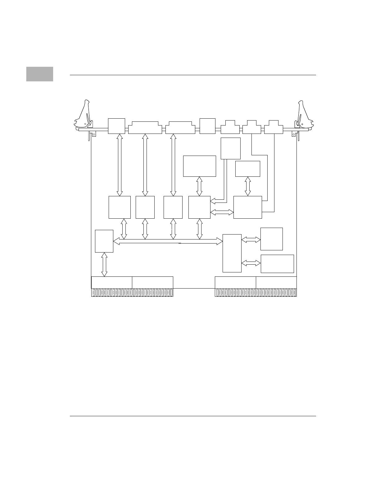
Figure 1-1. Block diagram
2166 9803
Ethernet SCSI
Video KBD/Mouse LPT 1 COM 2 COM 1
RJ45
Mini Dsub Dsub
DIN
Micro D Micro DMicro D
Ethernet
10/100
Ultra
SCSI
7880
Video
South
Bridge
(PIIx3)
Ultra
I/O
Bridge
J1 J2 J4 J5
North
DRAM
512K Cache
PCI Bus
256M
4 SIMMS
with Extended
Cacheability
Bridge
(TXC)
430HX
LM78
System
Monitor
On-board
IDE Hard Drive
or Flash
On-board
Floppy
PCI Bus
COM1
COM2
LTP1
Kbd/Mouse
USBx2
EIDE
EIDE
Floppy
SCSI - 3
SVGA
Ethernet
IDE
/