Intel OCT User guide

Type
User guide

Intel OCT is a powerful IP that allows you to dynamically calibrate I/O with reference to an external resistor. With support for up to 12 on-chip termination blocks, calibrated on-chip series termination, and calibrated on-chip parallel termination on all I/O pins, it offers exceptional signal integrity and reduces board space. Whether you're working with Stratix 10, Arria 10, or Cyclone 10 GX devices, the Intel OCT provides a reliable and efficient solution for your I/O calibration needs.

Intel OCT is a powerful IP that allows you to dynamically calibrate I/O with reference to an external resistor. With support for up to 12 on-chip termination blocks, calibrated on-chip series termination, and calibrated on-chip parallel termination on all I/O pins, it offers exceptional signal integrity and reduces board space. Whether you're working with Stratix 10, Arria 10, or Cyclone 10 GX devices, the Intel OCT provides a reliable and efficient solution for your I/O calibration needs.

OCT Intel® FPGA IP User Guide
Updated for Intel® Quartus® Prime Design Suite: 19.2
IP Version: 19.1
Online Version
Send Feedback ug-altera_oct
ID: 683708
Version: 2019.07.03
Contents
OCT Intel® FPGA IP User Guide...........................................................................................3
OCT Intel FPGA IP Features........................................................................................... 3
OCT Intel FPGA IP Overview.......................................................................................... 4
RZQ Pin.............................................................................................................4
OCT Block..........................................................................................................4
OCT Logic.......................................................................................................... 4
OCT Intel FPGA IP Functional Description........................................................................ 5
Power-Up Mode Interfaces................................................................................... 7
User Mode OCT...................................................................................................8
OCT Intel FPGA IP Design Example............................................................................... 10
Generating the Intel Quartus® Prime Design Example............................................ 10
OCT Intel FPGA IP References...................................................................................... 11
OCT Intel FPGA IP Parameter Settings..................................................................11
OCT Intel FPGA IP Signals.................................................................................. 11
QSF Assignments.............................................................................................. 12
IP Migration Flow for Arria V, Cyclone V, and Stratix V Devices................................ 13
OCT Intel FPGA IP User Guide Archives......................................................................... 13
Document Revision History for OCT Intel FPGA IP User Guide........................................... 14
Contents
OCT Intel® FPGA IP User Guide Send Feedback
2
OCT Intel® FPGA IP User Guide
The OCT Intel FPGA IP allows you to dynamically calibrate I/O with reference to an
external resistor. The OCT IP improves signal integrity, reduces board space, and is
necessary for communicating with external devices such as memory interfaces.
The OCT IP is available for Intel Stratix® 10, Intel Arria® 10, and Intel Cyclone® 10
GX devices. If you are migrating designs from Stratix V, Arria V, and Cyclone V
devices, you need to migrate the IP. For more details, refer to the related information.
Related Information
Migrating Your ALTOCT IP to the OCT Intel FPGA IP on page 13
Provides steps to migrate your ALTOCT IP core to the OCT IP core.
Dynamic Calibrated On-Chip Termination (ALTOCT) IP Core User Guide
Provides information about the ALTOCT IP core.
Introduction to Intel FPGA IP Cores
Provides general information about all Intel FPGA IP cores, including
parameterizing, generating, upgrading, and simulating IP cores.
Creating Version-Independent IP and Platform Designer Simulation Scripts
Create simulation scripts that do not require manual updates for software or IP
version upgrades.
Project Management Best Practices
Guidelines for efficient management and portability of your project and IP files.
OCT Intel FPGA IP User Guide Archives on page 13
Provides a list of user guides for previous versions of the OCTIntel FPGA IP.
OCT Intel FPGA IP Features
The OCT IP supports the following features:
Support for up to 12 on-chip termination (OCT) blocks
Support for calibrated on-chip series termination (RS) and calibrated on-chip
parallel termination (RT) on all I/O pins
Calibrated termination values of 25 Ω and 50 Ω
Support for OCT calibration in power-up and user modes
683708 | 2019.07.03
Send Feedback
Intel Corporation. All rights reserved. Intel, the Intel logo, and other Intel marks are trademarks of Intel
Corporation or its subsidiaries. Intel warrants performance of its FPGA and semiconductor products to current
specifications in accordance with Intel's standard warranty, but reserves the right to make changes to any
products and services at any time without notice. Intel assumes no responsibility or liability arising out of the
application or use of any information, product, or service described herein except as expressly agreed to in
writing by Intel. Intel customers are advised to obtain the latest version of device specifications before relying
on any published information and before placing orders for products or services.
*Other names and brands may be claimed as the property of others.
ISO
9001:2015
Registered
OCT Intel FPGA IP Overview
Figure 1. OCT IP Top-Level Diagram
This figure shows the top-level diagram of the OCT IP.
OCT Block OCT Logic
rzqin
OCT Intel® FPGA IP
Table 1. OCT IP Components
Component Description
RZQ pin Dual-purpose pin.
When used with OCT, the pin connects to an external reference resistor to calculate the
calibration codes to implement the required impedance.
OCT block Generates and sends calibration code words to the I/O buffer blocks.
OCT logic Receives the calibration code words serially from the OCT block and sends the calibration
code words in parallel to the buffers.
RZQ Pin
Each OCT block has one RZQ pin.
RZQ pins are dual-purpose pins. If the pins are not connected to the OCT block,
you can use the pins as regular I/O pins.
Calibrated pins must have the same VCCIO voltage as the OCT block and the RZQ
pin. Calibrated pins connected to the same OCT block must have the same series
and parallel termination values.
You can apply location constraints on the RZQ pins to determine the placement of
the OCT block because the RZQ pin can only be connected to its corresponding
OCT block.
OCT Block
The OCT block is a component that generates calibration codes to terminate the I/Os.
During calibration, the OCT matches the impedance seen on the external resistor
through the rzqin port. Then, the OCT block generates two 16-bit calibration code
words—one word calibrates the series termination and the other word calibrates the
parallel termination. A dedicated bus sends the words serially to the OCT logic.
OCT Logic
The OCT block sends the calibration code words serially to the OCT logic through the
ser_data ports.
OCT Intel® FPGA IP User Guide
683708 | 2019.07.03
OCT Intel® FPGA IP User Guide Send Feedback
4
The enser signal, when triggered, specifies from which OCT block to read the
calibration code words. The calibration code words are then buffered into the serial-to-
parallel shift logic. After that, the s2pload signal automatically asserts to send the
calibration code words in parallel to the I/O buffers.
The calibration code words activate or deactivate the transistors in the I/O block,
which will emulate series or parallel resistance to match the impedance.
Figure 2. Internals of OCT Logic
I/O Block
OCT Logic Block
I/O Block
ser_data
clk
0
10
enser[11:0]
0 1
Clock
R
R
R
R
USRMODE
s2pload#
serial_load_en
s2pload
I/O 1 I/O 2
parallelterminationcontrol
seriesterminationcontrol
IOCSR
16
16
Serial to Parallel
Shift Logic
OCT Intel FPGA IP Functional Description
To meet DDR memory specification, Intel Stratix 10, Intel Arria 10, and Intel Cyclone
10 GX devices support on-chip series termination (RS OCT) and on-chip parallel
termination (RT OCT) for single-ended I/O standards. OCT can be supported on any
I/O bank. The VCCIO must be compatible for all I/Os in a given bank.
In an Intel Stratix 10, Intel Arria 10, or Intel Cyclone 10 GX device, there is one OCT
block in each I/O bank. Each OCT block requires an association with an external 240 Ω
reference resistor through an RZQ pin.
The RZQ pin shares the same VCCIO supply with the I/O bank where the pin is located.
An RZQ pin is a dual function I/O pin that you can use as a regular I/O if you do not
use OCT calibration. When you use the RZQ pin for OCT calibration, the RZQ pin
connects the OCT block to ground through an external 240 Ω resistor.
The following figures show how OCTs are connected in a single I/O column (in a daisy
chain). An OCT can calibrate an I/O belonging to any bank, provided that the bank is
in the same column and meets the voltage requirements. Because there are no
connections between columns, OCT can only be shared if the pins belong to the same
I/O column of the OCT.
OCT Intel® FPGA IP User Guide
683708 | 2019.07.03
Send Feedback OCT Intel® FPGA IP User Guide
5
Figure 3. OCT Bank-to-Bank Connections
OCT 1 ser_data*
OCT 2 ser_data*
OCT 0 ser_data*
00
01
1x
00
01
1x
00
01
1x
Sel[1]
Sel[0] Sel[0]
Sel[1] Sel[0]
Sel[1]
enser
Sel[1]
Enser_top
enser
Sel[1]
enser
Sel[1]
Sel[0]
Sel[0]
Sel[0]
Enser_top Enser_top
OCT Intel® FPGA IP User Guide
683708 | 2019.07.03
OCT Intel® FPGA IP User Guide Send Feedback
6
Figure 4. I/O Columns in Intel Quartus® Prime Pin Planner
This figure is an example. The layout varies between different Intel Stratix 10, Intel Arria 10, or Intel Cyclone
10 GX devices.
Power-Up Mode Interfaces
The OCT IP in power-up mode has two main interfaces:
One input interface connecting the FPGA RZQ pad to the OCT block
Two 16-bit words output which connect to I/O buffers
Figure 5. OCT Interfaces
OCT Intel® FPGA IP
To I/O Buffers
To I/O Buffers
RZQ PAD
Series
Termination
Parallel
Termination
OCT Intel® FPGA IP User Guide
683708 | 2019.07.03
Send Feedback OCT Intel® FPGA IP User Guide
7
User Mode OCT
User mode OCT operates the same way as power-up OCT mode, with the addition of
user controllability.
Figure 6. FSM Signals
This figure shows a finite state machine (FSM) in the core controls the dedicated user signals on the OCT block.
The FSM ensures that the OCT block calibrates or sends controlling code words as per your request.
OCT Block
NCLRUSER
CLKENUSR
CLKUSR
CLKUSR
Core FSM
The Fitter does not infer a user-mode OCT. If you want your OCT block to use the user
mode OCT feature, you must generate the OCT IP. However, because of hardware
limitations, you can only use one OCT IP in user mode OCT in your design.
Note: A single OCT IP can control up to 12 OCT blocks.
The FSM provides the following signals:
clock
reset
s2pload
calibration_busy
calibration_shift_busy
calibration_request
Note: These signals are only available in user-mode and not power-up mode.
Related Information
OCT Intel FPGA IP Signals on page 11
Provides more information about the FSM signals.
OCT Intel® FPGA IP User Guide
683708 | 2019.07.03
OCT Intel® FPGA IP User Guide Send Feedback
8
Core FSM
Figure 7. FSM Flow
CAL
Check Mask Bit
Series Shift
Update
Pending Bit
DONE
Shift Mask Bit
IDLE
calibration_request
2000
Cycles
32
Cycles
Number of
OCT
Table 2. FSM States
State Description
IDLE When you set the calibration_request vector, the FSM moves from IDLE state to CAL
state. Keep the calibration_request vector at its value for two clock cycles. After two clock
cycles, the FSM contains a copy of the vector. You must reset the vector to avoid reinitiating the
calibration process.
CAL During this state, the FSM checks which bits in the calibration_request vector were
asserted and services them. The corresponding OCT blocks starts the calibration process that
takes around 2,000 clock cycles to complete. After calibration completes, the
calibration_busy signal is released.
Check Mask bit The FSM checks each bit in the vector if the bit is set or not.
continued...
OCT Intel® FPGA IP User Guide
683708 | 2019.07.03
Send Feedback OCT Intel® FPGA IP User Guide
9
State Description
Shift Mask bit This state simply loops over all the bits in the vector until it hits a 1.
Series Shift This state serially sends the termination code from the OCT block to the termination logic. It
takes 32 cycles to complete the transfer. After each transfer, the FSM check for any pending bits
in the vector and services them accordingly.
Update Pending Bit The pending register holds bits that corresponds to every OCT block in the OCT Intel FPGA IP.
This state updates the pending register by resetting the serviced request.
DONE When the calibration_shift_busy signal is deasserted, you can assert s2pload
automatically asserts to transfer the new termination codes into the buffers. The s2pload
signal asserts for at least 25 ns.
Because of hardware limitations, you cannot request another calibration until all bits in
calibration_shift_busy vector are low.
OCT Intel FPGA IP Design Example
The OCT IP can generate a design example that matches the same configuration
chosen for the IP.
The design example is a simple design that does not target any specific application.
You can use the design example as a reference on how to instantiate the IP.
To generate the design example files, turn on the Generate Example Design option
in the Generation dialog box during IP generation.
Note: The OCT IP does not support VHDL generation.
The software generates the <instance>_example_design directory along with
the IP, where <instance> is the name of your IP.
The <instance>_example_design directory contains the
make_qii_design.tcl scripts.
Note: The .qsys files are for internal use during design example generation only. You
cannot edit the files.
Generating the Intel Quartus® Prime Design Example
The make_qii_design.tcl script generates a synthesizable design example along
with an Intel Quartus® Prime project, ready for compilation.
To generate synthesizable design example, follow these steps.
1. After generating the IP together with the design example files, run the following
script at the command prompt: quartus_sh -t make_qii_design.tcl.
2. If you wan to specify an exact device to use, use the following command:
quartus_sh -t make_qii_design.tcl <device_name>.
The script generates a qii directory that contains the ed_synth.qpf project file. You
can open and compile this project in the Intel Quartus Prime software.
OCT Intel® FPGA IP User Guide
683708 | 2019.07.03
OCT Intel® FPGA IP User Guide Send Feedback
10
OCT Intel FPGA IP References
OCT Intel FPGA IP Parameter Settings
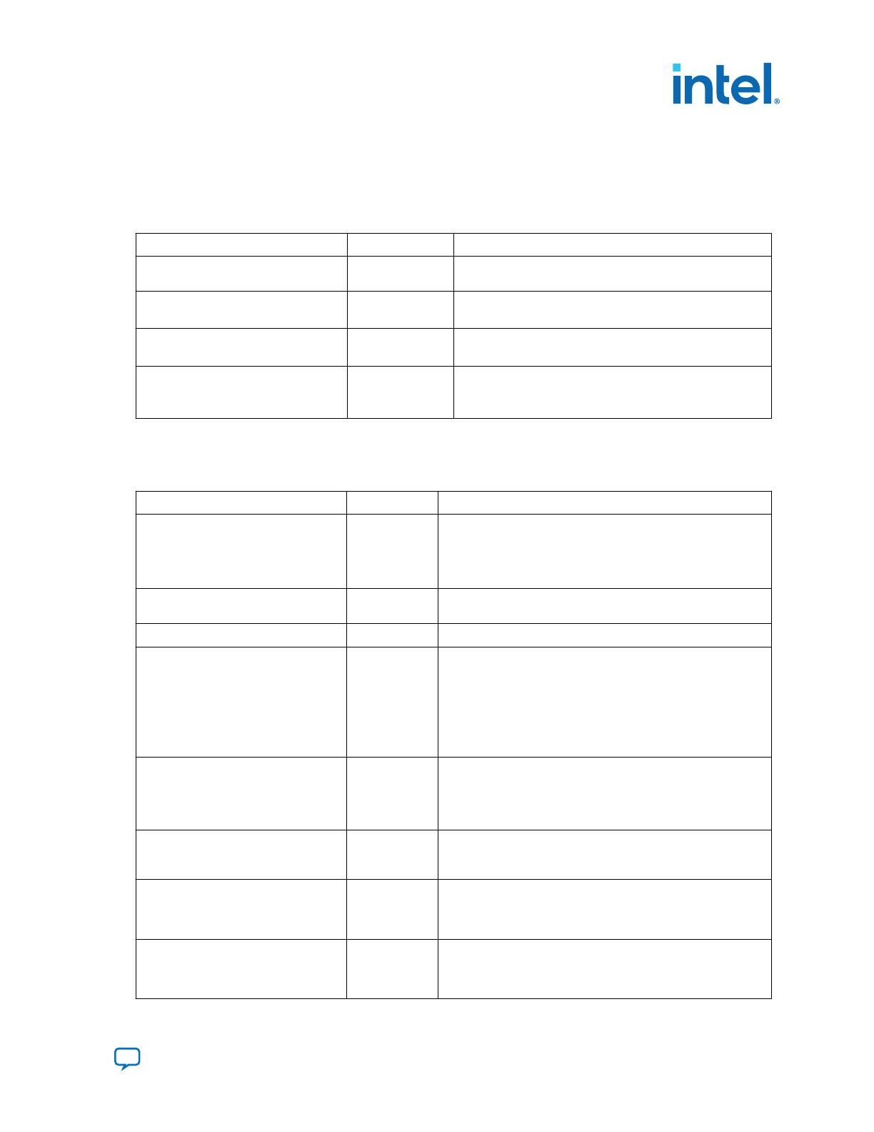
Table 3. OCT IP Parameters
Name Value Description
Number of OCT blocks 1 to 12 Specifies the number of OCT blocks to be generated. The
default value is 1.
Use backwards-compatible port
names
• On
• Off
Check this to use legacy top-level names compatible with
the ALTOCT IP. This parameter is disabled by default.
OCT mode • Power-up
• User
Specifies whether OCT is user-controllable or not. The
default value is Power-up.
OCT block x calibration mode • Single
• Double
• POD
Specifies the calibration mode for the OCT. X corresponds to
the number of the OCT block. The default value is Single.
OCT Intel FPGA IP Signals
Table 4. Input Interface Signals
Signal Name Direction Description
rzqin Input Input connection from RZQ pad to the OCT block. RZQ pad is
connected to an external resistance. The OCT block uses
impedance connected to the rzqin port as a reference to
generate the calibration code.
This signal is available for power-up and user modes.
clock Input Input clock for user mode OCT. The clock must be 20 MHz or
less.
reset Input Input reset signal. Reset is synchronous.
calibration_request Input Input vector for [NUMBER_OF_OCT:0]. Every bit corresponds
to an OCT block. When a bit is set to 1, the corresponding OCT
calibrates, then serially shift the code word into the termination
logic block. The request has to be held for two clock cycles.
Due to hardware limitations, you must wait until the
calibration_shift_busy vector to be zero until another
request is issued; otherwise your request will not be
processed.
calibration_shift_busy Output Output vector for [NUMBER_OF_OCT:0] indicating which OCT
block is currently working on calibration and shifting
termination codes to the termination logic block. When a bit is
1, it indicates that an OCT block is calibrating and shifting the
code word to the termination logic block.
calibration_busy Output Output vector for [NUMBER_OF_OCT:0] indicating which OCT
block is currently working on calibration. When a bit is 1, it
indicates that an OCT block is calibrating
oct_<x>_series_termination
control[15:0]
Output 16-bit output signal, with <x> ranging from 0 to 11. This
signal connects to the seriesterminationcontrol port on
the input/output buffer. This port sends the series termination
code that calibrates Rs.
oct_<x>_parallel_termination_
control[15:0]
Output 16-bit output signal, with <x> ranging from 0 to 11. This
signal connects to the parallelterminationcontrol port
on the input/output buffer. This port sends the parallel
termination code that calibrates Rt.
OCT Intel® FPGA IP User Guide
683708 | 2019.07.03
Send Feedback OCT Intel® FPGA IP User Guide
11
QSF Assignments
Intel Stratix 10, Intel Arria 10, and Intel Cyclone 10 GX devices have the following
termination-related Intel Quartus Prime settings file (.qsf) assignments:
INPUT_TERMINATION
OUTPUT_TERMINATION
TERMINATION_CONTROL_BLOCK
RZQ_GROUP
Table 5. QSF Assignments
QSF Assignment Details
INPUT_TERMINATION
OUTPUT_TERMINATION
The input/output termination assignment specifies the termination value in ohm on the pin
in question.
Example:
set_instance_assignment -name INPUT_TERMINATION <value> -to <pin name>
set_instance_assignment -name OUTPUT_TERMINATION <value> -to <pin name>
To enable the series/parallel termination ports, include these assignments, which specify
the series and parallel termination values for the pins.
Make sure to connect the seriesterminationcontrol and
parallelterminationcontrol ports from the OCT Intel FPGA IP to the GPIO Intel FPGA
IP.
Example:
set_instance_assignment -name INPUT_TERMINATION "PARALLEL <VALUE> OHM WITH
CALIBRATION" -to <pin>
set_instance_assignment -name OUTPUT_TERMINATION "SERIES <VALUE> OHM WITH
CALIBRATION" -to <pin>
TERMINATION_CONTROL_BL
OCK
Directs the Fitter to make the proper connection from the desired OCT block to the
specified pins. This assignment is useful when I/O buffers are not explicitly instantiated and
you need to associate the pins with a specific OCT block.
Example:
set_instance_assignment -name TERMINATION_CONTROL_BLOCK <desired OCT BLK> -to <pin
name>
RZQ_GROUP This assignment is supported in Intel Stratix 10, Intel Arria 10, and Intel Cyclone 10 GX
devices only. This assignment creates an OCT IP without modifying the RTL.
The Fitter searches for the rzq pin name in the netlist. If the pin does not exist, the Fitter
creates the pin name along with the OCT IP and its corresponding connections. This allows
you to create a group of pins to be calibrated by an existing or non-existing OCT and the
Fitter ensures the legality of the design.
Example:
set_instance_assignment -name RZQ_GROUP <rzq pin name> -to <pin name>
Termination can exist on input and output buffers, and sometimes simultaneously.
There are two methods to associate pin groups with an OCT block:
Use a .qsf assignment to indicate which pin (bus) is associated with which OCT
block. You can use the TERMINATION_CONTROL_BLOCK or
RZQ_GROUPassignment. The former assignment associates a pin with an OCT
instantiated in the RTL while the latter associates the pin with a newly created
OCT without modifying the RTL.
Instantiate the I/O buffer primitives at the top level and connect them to the
appropriate OCT blocks.
OCT Intel® FPGA IP User Guide
683708 | 2019.07.03
OCT Intel® FPGA IP User Guide Send Feedback
12
Note: All I/O banks with the same VCCIO can share one OCT block even if that particular I/O
bank has its own OCT block. You can connect any number of I/O pins that support
calibrated termination to an OCT block. Ensure that you connect I/Os with compatible
configuration to an OCT block. You must also ensure that the OCT block and its
corresponding I/Os have the same VCCIO and series or parallel termination values.
With these settings, the Fitter places the I/Os and OCT block in the same column. The
Intel Quartus Prime software generates warning messages if there is no pin connected
to the block.
IP Migration Flow for Arria V, Cyclone V, and Stratix V Devices
The IP migration flow allows you to migrate the ALTOCT IP of Arria V, Cyclone V, and
Stratix V devices to the OCT Intel FPGA IP of Intel Stratix 10, Intel Arria 10, or Intel
Cyclone 10 GX devices.
The IP migration flow configures the OCT IP to match the settings of the ALTOCT IP,
allowing you to regenerate the IP.
Note: This IP supports the IP migration flow in single OCT calibration mode only. If you are
using double or POD calibration mode, you do not need to migrate the IP.
Migrating Your ALTOCT IP to the OCT Intel FPGA IP
To migrate your ALTOCT IP to the OCT IP, follow these steps:
1. Open your ALTOCT IP in the IP Catalog.
2. In Currently selected device family, select Stratix 10, Arria 10, or Cyclone
10 GX.
3. Click Finish to open the OCT IP in the parameter editor.
The parameter editor configures the OCT IP settings similar to the ALTOCT IP
settings.
4. If there are any incompatible settings between the two, select new supported
settings.
5. Click Finish to regenerate the IP.
6. Replace your ALTOCT IP instantiation in RTL with the OCT IP.
Note: The OCT IP port names may not match the ALTOCT IP port names. Therefore, simply
changing the IP name in the instantiation is not sufficient.
OCT Intel FPGA IP User Guide Archives
If an IP core version is not listed, the user guide for the previous IP core version applies.
IP Core Version User Guide
17.1 Intel FPGA OCT IP Core User Guide
OCT Intel® FPGA IP User Guide
683708 | 2019.07.03
Send Feedback OCT Intel® FPGA IP User Guide
13
Document Revision History for OCT Intel FPGA IP User Guide
Document Version Intel Quartus
Prime Version
IP Version Changes
2019.07.03 19.2 19.1 Added support for Intel Stratix 10 devices.
Updated the following IP names:
"Intel FPGA OCT" to "OCT Intel FPGA IP"
"Intel FPGA GPIO" to "GPIO Intel FPGA IP"
Updated the s2pload signal:
Removed s2pload from available user signals.
Updated descriptions regarding the s2pload
signal behavior.
Date Version Changes
November 2017 2017.11.06 Added support for Intel Cyclone 10 GX devices.
Renamed Altera OCT IP core to Intel FPGA OCT IP core.
Renamed Qsys to Platform Designer.
Updated text for additional Intel rebranding.
May 2017 2017.05.08 Rebranded as Intel.
December, 2015 2015.12.07 Changed instances of "megafunction" to "IP core".
Changed instances of Quartus II to Quartus Prime.
Various edits to contents and links to improve style and clarity.
August, 2014 2014.08.18 Added information about OCT calibration in user mode.
Updated the IP core signals and parameters:
core_rzqin_export changed to rzqin
core_series_termination_control_export changed to
oct_<x>_series_termination control[15:0]
core_parallel_termination_control_export changed to
oct_<x>_parallel_termination_control[15:0]
November, 2013 2013.11.29 Initial release.
OCT Intel® FPGA IP User Guide
683708 | 2019.07.03
OCT Intel® FPGA IP User Guide Send Feedback
14
  • Page 1 1
  • Page 2 2
  • Page 3 3
  • Page 4 4
  • Page 5 5
  • Page 6 6
  • Page 7 7
  • Page 8 8
  • Page 9 9
  • Page 10 10
  • Page 11 11
  • Page 12 12
  • Page 13 13
  • Page 14 14

Intel OCT User guide

Type
User guide

Intel OCT is a powerful IP that allows you to dynamically calibrate I/O with reference to an external resistor. With support for up to 12 on-chip termination blocks, calibrated on-chip series termination, and calibrated on-chip parallel termination on all I/O pins, it offers exceptional signal integrity and reduces board space. Whether you're working with Stratix 10, Arria 10, or Cyclone 10 GX devices, the Intel OCT provides a reliable and efficient solution for your I/O calibration needs.

Ask a question and I''ll find the answer in the document

Finding information in a document is now easier with AI