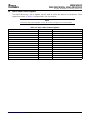
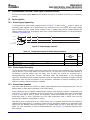
Texas Instruments SM320C6455-EP User manual
- Category
- Motherboards
- Type
- User manual

SM320C6455-EP
FIXED-POINT DIGITAL SIGNAL PROCESSOR
Data Manual
JANUARY 2008
SPRS462B

SM320C6455-EP
FIXED-POINT DIGITAL SIGNAL PROCESSOR
Data Manual
Literature Number: SPRS462B
SEPTEMBER 2007 – Revised JANUARY 2008
PRODUCTION DATA information is current as of publication date.
Products conform to specifications per the terms of the Texas
Instruments standard warranty. Production processing does not
necessarily include testing of all parameters.

Contents
SM320C6455-EP
FIXED-POINT DIGITAL SIGNAL PROCESSOR
SPRS462B – SEPTEMBER 2007 – REVISED JANUARY 2008
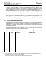
1 Features .............................................................................................................................. 7
1.1 ZTZ/GTZ BGA Package (Bottom View) ................................................................................... 8
1.2 Description .................................................................................................................... 8
1.3 Functional Block Diagram ................................................................................................. 10
2 Device Overview ................................................................................................................. 11
2.1 Device Characteristics ..................................................................................................... 11
2.2 CPU (DSP Core) Description ............................................................................................. 12
2.3 Memory Map Summary .................................................................................................... 15
2.4 Boot Sequence ............................................................................................................. 17
2.4.1 Boot Modes Supported ......................................................................................... 17
2.4.2 2nd-Level Bootloaders .......................................................................................... 19
2.5 Pin Assignments ............................................................................................................ 20
2.5.1 Pin Map ........................................................................................................... 20
2.6 Signal Groups Description ................................................................................................ 24
2.7 Terminal Functions ......................................................................................................... 30
2.8 Development ................................................................................................................ 55
2.8.1 Development Support ........................................................................................... 55
2.8.2 Device Support .................................................................................................. 55
2.8.2.1 Device and Development-Support Tool Nomenclature ........................................ 55
2.8.2.2 Documentation Support ............................................................................. 56
3 Device Configuration .......................................................................................................... 59
3.1 Device Configuration at Device Reset ................................................................................... 59
3.2 Peripheral Configuration at Device Reset ............................................................................... 61
3.3 Peripheral Selection After Device Reset ................................................................................ 63
3.4 Device State Control Registers ........................................................................................... 65
3.4.1 Peripheral Lock Register Description ......................................................................... 66
3.4.2 Peripheral Configuration Register 0 Description ............................................................ 67
3.4.3 Peripheral Configuration Register 1 Description ............................................................ 69
3.4.4 Peripheral Status Registers Description ...................................................................... 70
3.4.5 EMAC Configuration Register (EMACCFG) Description ................................................... 73
3.4.6 Emulator Buffer Powerdown Register (EMUBUFPD) Description ........................................ 74
3.5 Device Status Register Description ...................................................................................... 75
3.6 JTAG ID (JTAGID) Register Description ................................................................................ 77
3.7 Pullup/Pulldown Resistors ................................................................................................. 78
3.8 Configuration Examples ................................................................................................... 78
4 System Interconnect ........................................................................................................... 81
4.1 Internal Buses, Bridges, and Switch Fabrics ........................................................................... 81
4.2 Data Switch Fabric Connections ......................................................................................... 82
4.3 Configuration Switch Fabric ............................................................................................... 84
4.4 Bus Priorities ................................................................................................................ 86
5 C64x+ Megamodule ............................................................................................................ 87
5.1 Memory Architecture ....................................................................................................... 87
5.2 Memory Protection ......................................................................................................... 90
5.3 Bandwidth Management ................................................................................................... 90
5.4 Power-Down Control ....................................................................................................... 91
5.5 Megamodule Resets ....................................................................................................... 91
5.6 Megamodule Revision ..................................................................................................... 92
5.7 C64x+ Megamodule Register Description(s) ........................................................................... 93
6 Device Operating Conditions ............................................................................................. 101
6.1 Absolute Maximum Ratings Over Operating Case Temperature Range (Unless Otherwise Noted) .......... 101
Contents 3

SM320C6455-EP
FIXED-POINT DIGITAL SIGNAL PROCESSOR
SPRS462B – SEPTEMBER 2007 – REVISED JANUARY 2008
6.2 Recommended Operating Conditions .................................................................................. 101
6.3 Electrical Characteristics Over Recommended Ranges of Supply Voltage and Operating Case
Temperature (Unless Otherwise Noted) ............................................................................... 103
7 C64x+ Peripheral Information and Electrical Specifications ................................................... 105
7.1 Parameter Information ................................................................................................... 105
7.1.1 3.3-V Signal Transition Levels ............................................................................... 105
7.1.2 3.3-V Signal Transition Rates ................................................................................ 105
7.1.3 Timing Parameters and Board Routing Analysis .......................................................... 106
7.2 Recommended Clock and Control Signal Transition Behavior ..................................................... 107
7.3 Power Supplies ........................................................................................................... 107
7.3.1 Power-Supply Sequencing .................................................................................... 107
7.3.2 Power-Supply Decoupling .................................................................................... 107
7.3.3 Power-Down Operation ....................................................................................... 107
7.3.4 Preserving Boundary-Scan Functionality on RGMII and DDR2 Memory Pins ......................... 108
7.4 Enhanced Direct Memory Access (EDMA3) Controller .............................................................. 109
7.4.1 EDMA3 Device-Specific Information ........................................................................ 110
7.4.2 EDMA3 Channel Synchronization Events .................................................................. 110
7.4.3 EDMA3 Peripheral Register Description(s) ................................................................. 111
7.5 Interrupts ................................................................................................................... 124
7.5.1 Interrupt Sources and Interrupt Controller .................................................................. 124
7.5.2 External Interrupts Electrical Data/Timing .................................................................. 127
7.6 Reset Controller ........................................................................................................... 128
7.6.1 Power-on Reset ( POR Pin) ................................................................................... 128
7.6.2 Warm Reset ( RESET Pin) .................................................................................... 129
7.6.3 Max Reset ....................................................................................................... 130
7.6.4 System Reset ................................................................................................... 130
7.6.5 CPU Reset ...................................................................................................... 130
7.6.6 Reset Priority ................................................................................................... 131
7.6.7 Reset Controller Register ..................................................................................... 132
7.6.7.1 Reset Type Status Register Description ......................................................... 132
7.6.8 Reset Electrical Data/Timing ................................................................................. 133
7.7 PLL1 and PLL1 Controller ............................................................................................... 136
7.7.1 PLL1 Controller Device-Specific Information ............................................................... 137
7.7.1.1 Internal Clocks and Maximum Operating Frequencies ......................................... 137
7.7.1.2 PLL1 Controller Operating Modes ................................................................ 138
7.7.1.3 PLL1 Stabilization, Lock, and Reset Times ...................................................... 138
7.7.2 PLL1 Controller Memory Map ................................................................................ 139
7.7.3 PLL1 Controller Register Descriptions ...................................................................... 140
7.7.3.1 PLL1 Control Register .............................................................................. 140
7.7.3.2 PLL Multiplier Control Register .................................................................... 141
7.7.3.3 PLL Pre-Divider Control Register ................................................................. 142
7.7.3.4 PLL Controller Divider 4 Register ................................................................. 143
7.7.3.5 PLL Controller Divider 5 Register ................................................................. 144
7.7.3.6 PLL Controller Command Register ............................................................... 145
7.7.3.7 PLL Controller Status Register .................................................................... 146
7.7.3.8 PLL Controller Clock Align Control Register ..................................................... 147
7.7.3.9 PLLDIV Ratio Change Status Register ........................................................... 148
7.7.3.10 SYSCLK Status Register ......................................................................... 149
7.7.4 PLL1 Controller Input and Output Clock Electrical Data/Timing ......................................... 150
7.8 PLL2 and PLL2 Controller ............................................................................................... 151
7.8.1 PLL2 Controller Device-Specific Information ............................................................... 152
7.8.1.1 Internal Clocks and Maximum Operating Frequencies ......................................... 152
7.8.1.2 PLL2 Controller Operating Modes ................................................................ 152
Contents 4 Submit Documentation Feedback

SM320C6455-EP
FIXED-POINT DIGITAL SIGNAL PROCESSOR
SPRS462B – SEPTEMBER 2007 – REVISED JANUARY 2008
7.8.2 PLL2 Controller Memory Map ................................................................................ 153
7.8.3 PLL2 Controller Register Descriptions ...................................................................... 153
7.8.3.1 PLL Controller Divider 1 Register ................................................................. 154
7.8.3.2 PLL Controller Command Register ............................................................... 155
7.8.3.3 PLL Controller Status Register .................................................................... 156
7.8.3.4 PLL Controller Clock Align Control Register ..................................................... 156
7.8.3.5 PLLDIV Ratio Change Status Register ........................................................... 157
7.8.3.6 SYSCLK Status Register ........................................................................... 158
7.8.4 PLL2 Controller Input Clock Electrical Data/Timing ....................................................... 159
7.9 DDR2 Memory Controller ................................................................................................ 160
7.9.1 DDR2 Memory Controller Device-Specific Information ................................................... 160
7.9.2 DDR2 Memory Controller Peripheral Register Description(s) ............................................ 161
7.9.3 DDR2 Memory Controller Electrical Data/Timing .......................................................... 161
7.10 External Memory Interface A (EMIFA) ................................................................................. 162
7.10.1 EMIFA Device-Specific Information .......................................................................... 162
7.10.2 EMIFA Peripheral Register Description(s) .................................................................. 163
7.10.3 EMIFA Electrical Data/Timing ................................................................................ 164
7.10.3.1 Asynchronous Memory Timing .................................................................. 165
7.10.3.2 Programmable Synchronous Interface Timing ................................................ 168
7.10.4 HOLD/ HOLDA Timing ......................................................................................... 171
7.10.5 BUSREQ Timing ............................................................................................... 172
7.11 I2C Peripheral ............................................................................................................. 173
7.11.1 I2C Device-Specific Information .............................................................................. 173
7.11.2 I2C Peripheral Register Description(s) ...................................................................... 175
7.11.3 I2C Electrical Data/Timing .................................................................................... 176
7.11.3.1 Inter-Integrated Circuits (I2C) Timing .......................................................... 176
7.12 Host-Port Interface (HPI) Peripheral ................................................................................... 179
7.12.1 HPI Device-Specific Information ............................................................................. 179
7.12.2 HPI Peripheral Register Description(s) ...................................................................... 179
7.12.3 HPI Electrical Data/Timing .................................................................................... 180
7.13 Multichannel Buffered Serial Port (McBSP) ........................................................................... 190
7.13.1 McBSP Device-Specific Information ......................................................................... 191
7.13.1.1 McBSP Peripheral Register Description(s) ..................................................... 191
7.13.2 McBSP Electrical Data/Timing ............................................................................... 193
7.13.2.1 Multichannel Buffered Serial Port (McBSP) Timing ......................................... 193
7.14 Ethernet MAC (EMAC) ................................................................................................... 200
7.14.1 EMAC Device-Specific Information .......................................................................... 201
7.14.2 EMAC Peripheral Register Description(s) .................................................................. 204
7.14.3 EMAC Electrical Data/Timing ................................................................................. 208
7.14.3.1 EMAC MII and GMII Electrical Data/Timing .................................................. 208
7.14.3.2 EMAC RMII Electrical Data/Timing .............................................................. 211
7.14.3.3 EMAC RGMII Electrical Data/Timing ............................................................ 213
7.14.4 Management Data Input/Output (MDIO) ................................................................... 216
7.14.4.1 MDIO Device-Specific Information .............................................................. 216
7.14.4.2 MDIO Peripheral Register Description(s) ....................................................... 216
7.14.4.3 MDIO Electrical Data/Timing ..................................................................... 217
7.15 Timers ...................................................................................................................... 218
7.15.1 Timers Device-Specific Information .......................................................................... 218
7.15.2 Timers Peripheral Register Description(s) .................................................................. 218
7.15.3 Timers Electrical Data/Timing ................................................................................ 219
7.16 Enhanced Viterbi-Decoder Coprocessor (VCP2) ..................................................................... 220
7.16.1 VCP2 Device-Specific Information ........................................................................... 220
7.16.2 VCP2 Peripheral Register Description(s) ................................................................... 220
Contents 5

SM320C6455-EP
FIXED-POINT DIGITAL SIGNAL PROCESSOR
SPRS462B – SEPTEMBER 2007 – REVISED JANUARY 2008
7.17 Enhanced Turbo Decoder Coprocessor (TCP2) ...................................................................... 221
7.17.1 TCP2 Device-Specific Information ........................................................................... 221
7.17.2 TCP2 Peripheral Register Description(s) ................................................................... 222
7.18 Peripheral Component Interconnect (PCI) ............................................................................ 223
7.18.1 PCI Device-Specific Information ............................................................................. 223
7.18.2 PCI Peripheral Register Description(s) ...................................................................... 224
7.18.3 PCI Electrical Data/Timing .................................................................................... 229
7.19 UTOPIA .................................................................................................................... 230
7.19.1 UTOPIA Device-Specific Information ........................................................................ 230
7.19.2 UTOPIA Peripheral Register Description(s) ................................................................ 230
7.19.3 UTOPIA Electrical Data/Timing .............................................................................. 231
7.20 Serial RapidIO (SRIO) Port .............................................................................................. 234
7.20.1 Serial RapidIO Device-Specific Information ................................................................ 234
7.20.2 Serial RapidIO Peripheral Register Description(s) ........................................................ 234
7.20.3 Serial RapidIO Electrical Data/Timing ....................................................................... 244
7.21 General-Purpose Input/Output (GPIO) ................................................................................. 246
7.21.1 GPIO Device-Specific Information ........................................................................... 246
7.21.2 GPIO Peripheral Register Description(s) ................................................................... 246
7.21.3 GPIO Electrical Data/Timing .................................................................................. 247
7.22 Emulation Features and Capability ..................................................................................... 248
7.22.1 Advanced Event Triggering (AET) ........................................................................... 248
7.22.2 Trace ............................................................................................................. 248
7.22.3 IEEE 1149.1 JTAG ............................................................................................. 249
7.22.3.1 JTAG Device-Specific Information ............................................................... 249
7.22.4 JTAG Peripheral Register Description(s) ................................................................... 249
7.22.5 JTAG Electrical Data/Timing ................................................................................. 249
Revision History ........................................................................................................................ 250
8 Mechanical Data ............................................................................................................... 251
8.1 Thermal Data .............................................................................................................. 251
8.2 Packaging Information ................................................................................................... 251
Contents 6 Submit Documentation Feedback

www.ti.com
1 Features
SM320C6455-EP
FIXED-POINT DIGITAL SIGNAL PROCESSOR
SPRS462B – SEPTEMBER 2007 – REVISED JANUARY 2008
Parameters
• Controlled Baseline
• Endianess: Little Endian, Big Endian
– One Assembly Site
– Test Site
• 64 Bit External Memory Interface (EMIFA)
– One Fabrication Site
– Glueless Interface to Asynchronous
Memories (SRAM, Flash, and EEPROM) and
• Enhanced Diminishing Manufacturing Sources
Synchronous Memories (SBSRAM, ZBT
(DMS) Support
SRAM)
• Enhanced Product-Change Notification
– Supports Interface to Standard Sync
• Qualification Pedigree
(1)
Devices and Custom Logic (FPGA, CPLD,
ASICs, etc.)
• High-Performance Fixed-Point DSP (C6455)
– 32M Byte Total Addressable External
– 1.39 ns, 1.17 ns, 1 ns, and 0.83 ns
Memory Space
Instruction Cycle Time
• Four 1x Serial RapidIO® Links (or One 4x),
– 1 GHz Clock Rate
v1.2 Compliant
– Eight 32 Bit Instructions/Cycle
– 1.25/2.5/3.125 Gbps Link Rates
– 9600 MIPS/MMACS (16 Bits)
– Message Passing, DirectIO Support, Error
– Commercial Temperature (0 ° C to 90 ° C)
Management Extensions, and Congestion
– Extended Temperature (–40 ° C to 105 ° C)
Control
– S-Temp (–55 ° C to 105 ° C)
– IEEE 1149.6 Compliant I/Os
• C64x+™ DSP Core
• DDR2 Memory Controller
– Dedicated SPLOOP Instruction
– Interfaces to DDR2-533 SDRAM
– Compact Instructions (16 Bit)
– 32 Bit/16 Bit, 533 MHz (data rate) Bus
– Instruction Set Enhancements
– 512M Byte Total Addressable External
– Exception Handling
Memory Space
• C64x+ Megamodule L1/L2 Memory
• EDMA3 Controller (64 Independent Channels)
Architecture:
• 32/16 Bit Host-Port Interface (HPI)
– 256K Bit (32K Byte) L1P Program Cache
• 32 Bit 33/66 MHz, 3.3 V Peripheral Component
(Direct Mapped)
Interconnect (PCI) Master/Slave Interface
– 256K Bit (32K Byte) L1D Data Cache
Conforms to PCI Local Bus Specification
[2-Way Set-Associative]
(version 2.3)
– 16M Bit (2096K Byte) L2 Unified Mapped
RAM/Cache (Flexible Allocation)
• One Inter-Integrated Circuit (I
2
C) Bus
– 256K Bit (32K Byte) L2 ROM
• Two McBSPs
– Time Stamp Counter
• 10/100/1000 Mb/s Ethernet MAC (EMAC)
• Enhanced VCP2
– IEEE 802.3 Compliant
– Supports Over 694 7.95 Kbps AMR
– Supports Multiple Media Independent
– Programmable Code Parameters
Interfaces (MII, GMII, RMII, and RGMII)
– Eight Independent Transmit (TX) and
• Enhanced Turbo Decoder Coprocessor (TCP2)
Eight Independent Receive (RX) Channels
– Supports up to Eight 2 Mbps 3GPP
(6 Iterations)
• Two 64 Bit General-Purpose Timers,
– Programmable Turbo Code and Decoding Configurable as Four 32 Bit Timers
• UTOPIA
(1) Component qualification in accordance with JEDEC and
industry standards to ensure reliable operation over an
– UTOPIA Level 2 Slave ATM Controller
extended temperature range. This includes, but is not limited
– 8 Bit Transmit and Receive Operations up
to, Highly Accelerated Stress Test (HAST) or biased 85/85,
to 50 MHz per Direction
temperature cycle, autoclave or unbiased HAST,
electromigration, bond intermetallic life, and mold compound
– User-Defined Cell Format up to 64 Bytes
life. Such qualification testing should not be viewed as
• 16 General-Purpose I/O (GPIO) Pins
justifying use of this component beyond specified
performance and environmental limits.
Please be aware that an important notice concerning availability, standard warranty, and use in critical applications of Texas
Instruments semiconductor products and disclaimers thereto appears at the end of this document.
C64x+, JTAG, C64x+, VelociTI, C6000, Code Composer Studio, DSP/BIOS, XDS are trademarks of Texas Instruments.
PRODUCTION DATA information is current as of publication date.
Copyright © 2007–2008, Texas Instruments Incorporated
Products conform to specifications per the terms of the Texas
Instruments standard warranty. Production processing does not
necessarily include testing of all parameters.

www.ti.com
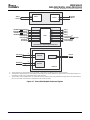
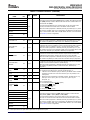
1.1 ZTZ/GTZ BGA Package (Bottom View)
ZTZ/GTZ 697-PIN BALL GRID ARRAY (BGA) PACKAGE
(BOTTOM VIEW)
A
2
B
1 3
4
5
6
7
8
9
10
11
12
13
14
15
16
17
18
19
20
21
22
23
24
25
26
C
D
E
F
G
H
J
K
L
M
N
P
R
T
U
V
W
Y
AA
AB
AC
AD
AE
AF
27
28
29
AG
AH
AJ
NOTE: The ZTZ mechanical package designator represents the version of the GTZ package with lead-free balls. For more detailed information,
see the Mechanical Data section of this document.
1.2 Description
SM320C6455-EP
FIXED-POINT DIGITAL SIGNAL PROCESSOR
SPRS462B – SEPTEMBER 2007 – REVISED JANUARY 2008
• System PLL and PLL Controller Boundary-Scan-Compatible
• Secondary PLL and PLL Controller, Dedicated • 697-Pin Ball Grid Array (BGA) Package
to EMAC and DDR2 Memory Controller (ZTZ or GTZ Suffix), 0.8 mm Ball Pitch
• Advanced Event Triggering (AET) Compatible • 0.09 µ m/7-Level Cu Metal Process (CMOS)
• Trace-Enabled Device • 3.3/1.8/1.5/1.25/1.2 V I/Os, 1.25/1.2 V Internal
• IEEE-1149.1 ( JTAG™)
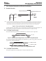
Figure 1-1 shows the SM320C6455-EP device 697-pin ball grid array package (bottom view).
Figure 1-1. ZTZ/GTZ BGA Package (Bottom View)
The C64x+™ DSPs (including the SM320C6455-EP device) are the highest-performance fixed-point DSP
generation in the C6000™ DSP platform. The C6455 device is based on the third-generation
high-performance, advanced VelociTI™ very-long-instruction-word (VLIW) architecture developed by
Texas Instruments (TI), making these DSPs an excellent choice for applications including video and
telecom infrastructure, imaging/medical, and wireless infrastructure (WI). The C64x+™ devices are
upward code-compatible from previous devices that are part of the C6000™ DSP platform.
Based on 90-nm process technology and with performance of up to 9600 million instructions per second
(MIPS) [or 9600 16 bit MMACs per cycle] at a 1.2-GHz clock rate, the C6455 device offers cost-effective
solutions to high-performance DSP programming challenges. The C6455 DSP possesses the operational
flexibility of high-speed controllers and the numerical capability of array processors.
Features8 Submit Documentation Feedback

www.ti.com
SM320C6455-EP
FIXED-POINT DIGITAL SIGNAL PROCESSOR
SPRS462B – SEPTEMBER 2007 – REVISED JANUARY 2008
The C64x+ DSP core employs eight functional units, two register files, and two data paths. Like the earlier
C6000 devices, two of these eight functional units are multipliers or .M units. Each C64x+ .M unit doubles
the multiply throughput versus the C64x core by performing four 16 bit x 16 bit multiply-accumulates
(MACs) every clock cycle. Thus, eight 16 bit x 16 bit MACs can be executed every cycle on the C64x+
core. At a 1.2-GHz clock rate, this means 9600 16 bit MMACs can occur every second. Moreover, each
multiplier on the C64x+ core can compute one 32 bit x 32 bit MAC or four 8 bit x 8 bit MACs every clock
cycle.
The C6455 device includes Serial RapidIO. This high bandwidth peripheral dramatically improves system
performance and reduces system cost for applications that include multiple DSPs on a board, such as
video and telecom infrastructures and medical/imaging.
The C6455 DSP integrates a large amount of on-chip memory organized as a two-level memory system.
The level-1 (L1) program and data memories on the C6455 device are 32KB each. This memory can be
configured as mapped RAM, cache, or some combination of the two. When configured as cache, L1
program (L1P) is a direct mapped cache where as L1 data (L1D) is a two-way set associative cache. The
level 2 (L2) memory is shared between program and data space and is 2096KB in size. L2 memory also
can be configured as mapped RAM, cache, or some combination of the two. The C64x+ Megamodule also
has a 32 bit peripheral configuration (CFG) port, an internal DMA (IDMA) controller, a system component
with reset/boot control, interrupt/exception control, a power-down control, and a free-running 32 bit timer
for time stamp.
The peripheral set includes: an inter-integrated circuit bus module (I2C); two multichannel buffered serial
ports (McBSPs); an 8 bit Universal Test and Operations PHY Interface for Asynchronous Transfer Mode
(ATM) Slave [UTOPIA Slave] port; two 64 bit general-purpose timers (also configurable as four 32 bit
timers); a user-configurable 16 bit or 32 bit host-port interface (HPI16/HPI32); a peripheral component
interconnect (PCI); a 16-pin general-purpose input/output port (GPIO) with programmable interrupt/event
generation modes; an 10/100/1000 Ethernet media access controller (EMAC), which provides an efficient
interface between the C6455 DSP core processor and the network; a management data input/output
(MDIO) module (also part of the EMAC) that continuously polls all 32 MDIO addresses in order to
enumerate all PHY devices in the system; a glueless external memory interface (64 bit EMIFA), which is
capable of interfacing to synchronous and asynchronous peripherals; and a 32 bit DDR2 SDRAM
interface.
The I2C ports on the C6455 allow the DSP to easily control peripheral devices and communicate with a
host processor. In addition, the standard multichannel buffered serial port (McBSP) may be used to
communicate with serial peripheral interface (SPI) mode peripheral devices.
The C6455 device has two high-performance embedded coprocessors [enhanced Viterbi Decoder
Coprocessor (VCP2) and enhanced Turbo Decoder Coprocessor (TCP2)] that significantly speed up
channel-decoding operations on-chip. The VCP2 operating at CPU clock divided-by-3 can decode over
694 7.95-Kbps adaptive multi-rate (AMR) [K = 9, R = 1/3] voice channels. The VCP2 supports constraint
lengths K = 5, 6, 7, 8, and 9, rates R = 3/4, 1/2, 1/3, 1/4, and 1/5 and flexible polynomials, while
generating hard decisions or soft decisions. The TCP2 operating at CPU clock divided-by-3 can decode
up to fifty 384-Kbps or eight 2-Mbps turbo encoded channels (assuming 6 iterations). The TCP2
implements the max*log-map algorithm and is designed to support all polynomials and rates required by
Third-Generation Partnership Projects (3GPP and 3GPP2), with fully programmable frame length and
turbo interleaver. Decoding parameters such as the number of iterations and stopping criteria are also
programmable. Communications between the VCP2/TCP2 and the CPU are carried out through the
EDMA3 controller.
The C6455 has a complete set of development tools which includes: a new C compiler, an assembly
optimizer to simplify programming and scheduling, and a Windows® debugger interface for visibility into
source code execution.
Submit Documentation Feedback Features 9

www.ti.com
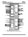
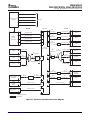
1.3 Functional Block Diagram
L2 Memory Controller
(Memory Protect/
Bandwidth Mgmt)
Serial Rapid
I/O
DDR2
Mem Ctlr
System
(B)
C64x+ DSP Core
Data Path B
B Register File
B31−B16
B15−B0
Instruction Fetch
Data Path A
A Register File
A31−A16
A15−A0
Device
Configuration
Logic
.L1 .S1
.M1
xx
xx
.D1 .D2
.M2
xx
xx
.S2 .L2
64
SBSRAM
SRAM
L1P Cache Direct-Mapped
32K Bytes
L1D Cache
2-Way
Set-Associative
32K Bytes Total
C6455
Primary Switched Central Resource
PLL1 and
PLL1
Controller
EMIFA
ZBT SRAM
HI
Boot Configuration
ROM/FLASH
I/O Devices
VCP2
I2C
GPIO16
(B)
16
McBSP0
(A)
Internal DMA
(IDMA)
M
e
g
a
m
o
d
u
l
e
L2
Cache
Memory
2096K
Bytes
L1P Memory Controller (Memory Protect/Bandwidth Mgmt)
TCP2
McBSP1
(A)
HPI (32/16)
(B)
Instruction
Decode
16-/32-bit
Instruction Dispatch
Control Registers
In-Circuit Emulation
DDR2 SDRAM
32
LO
Timer1
(C)
HI
LO
Timer0
(C)
PLL2 and
PLL2
Controller
(D)
EMAC
10/100/1000
SPLOOP Buffer
Power Control
L1D Memory Controller (Memory Protect/Bandwidth Mgmt)
Interrupt and Exception Controller
EDMA 3.0
L2 ROM
32K
Bytes
(E)
Secondary
Switched Central
Resource
A. McBSPs: Framing Chips − H.100, MVIP, SCSA, T1,E1; AC97 Devices; SPI Devices; Codecs
B. The PCI peripheral pins are muxed with some of the HPI peripheral pins and the UTOPIA address pins. For more detailed information, see the Device
Configuration section of this document.
C. Each of the TIMER peripherals (TIMER1 and TIMER0) is configurable as either two 64-bit general-purpose timers or two 32-bit general-purpose
timers or a watchdog timer.
D. The PLL2 controller also generates clocks for the EMAC.
E. When accessing the internal ROM of the DSP, the CPU frequency must always be less than 750 MHz.
MDIO
RMGII
(D)
GMII
RMII
MII
UTOPIA
(B)
PCI66
(B)
SM320C6455-EP
FIXED-POINT DIGITAL SIGNAL PROCESSOR
SPRS462B – SEPTEMBER 2007 – REVISED JANUARY 2008
Figure 1-2 shows the functional block diagram of the C6455 device.
Figure 1-2. Functional Block Diagram
10 Features Submit Documentation Feedback

www.ti.com
2 Device Overview
2.1 Device Characteristics
SM320C6455-EP
FIXED-POINT DIGITAL SIGNAL PROCESSOR
SPRS462B – SEPTEMBER 2007 – REVISED JANUARY 2008
Table 2-1 , provides an overview of the C6455 DSP. The tables show significant features of the C6455
device, including the capacity of on-chip RAM, the peripherals, the CPU frequency, and the package type
with pin count.
Table 2-1. Characteristics of the C6455 Processor
HARDWARE FEATURES C6455
EMIFA (64 bit bus width)
1
(clock source = AECLKIN or SYSCLK4)
DDR2 Memory Controller (32 bit bus width) [1.8 V I/O]
1
(clock source = CLKIN2)
EDMA3 (64 independent channels) [CPU/3 clock rate] 1
High-speed 1x/4x Serial Rapid IO Port 1
I2C 1
Peripherals
HPI (32- or 16 bit user selectable) 1 (HPI16 or HPI32)
Not all peripherals pins
are available at the same
PCI (32 bit), [66-MHz or 33-MHz] 1 (PCI66 or PCI33)
time (For more detail, see
McBSPs (internal CPU/6 or external clock source up
the Device Configuration
2
to 100 Mbps)
section).
UTOPIA (8 bit mode, 50-MHz, Slave-only) 1
10/100/1000 Ethernet MAC (EMAC) 1
Management Data Input/Output (MDIO) 1
64 Bit Timers (Configurable)
2 64 bit or 4 32 bit
(internal clock source = CPU/6 clock frequency)
General-Purpose Input/Output Port (GPIO) 16
VCP2 (clock source = CPU/3 clock frequency) 1
Decoder Coprocessors
TCP2 (clock source = CPU/3 clock frequency) 1
Size (Bytes) 2192K
32K-Byte (32KB) L1 Program Memory Controller
[SRAM/Cache]
On-Chip Memory
Organization 32KB Data Memory Controller [SRAM/Cache]
2096KB L2 Unified Memory/Cache
32KB L2 ROM
C64x+ Megamodule Megamodule Revision ID Register (address location:
See Section 5.6 , Megamodule Revision
Revision ID 0181 2000h)
See Section 3.6 , JTAG ID (JTAGID) Register
JTAG BSDL_ID JTAGID register (address location: 0x02A80008)
Description
Frequency MHz 720, 850, 1000 (1 GHz), and 1200 (1.2 GHz)
1.39 ns (C6455-720), 1.17 ns (C6455-850),
Cycle Time ns 1 ns (C6455 A-1000, -1000) [1-GHz CPU]
(1)
0.83 ns (C6455-1200) [1.2-GHz CPU]
1.25 V (A-1000/-1000/-1200)
Core (V)
1.2 V (-850/-720)
Voltage
1.25/1.2 [RapidIO],
I/O (V) 1.5/1.8 [EMAC RGMII], and
1.8 and 3.3 V [I/O Supply Voltage]
PLL1 and PLL1
CLKIN1 frequency multiplier Bypass (x1), x15, x20, x25, x30, x32
Controller Options
CLKIN2 frequency multiplier
PLL2 x20
[DDR2 Memory Controller and EMAC support only]
697-Pin Flip-Chip Plastic BGA (ZTZ)
BGA Package 24 x 24 mm
697-Pin Flip-Chip Plastic BGA (GTZ)
(1) The extended temperature device's (A-1000) electrical characteristics and ac timings are the same as those for the corresponding
commercial temperature devices (-1000).
Submit Documentation Feedback Device Overview 11

www.ti.com
2.2 CPU (DSP Core) Description
SM320C6455-EP
FIXED-POINT DIGITAL SIGNAL PROCESSOR
SPRS462B – SEPTEMBER 2007 – REVISED JANUARY 2008
Table 2-1. Characteristics of the C6455 Processor (continued)
HARDWARE FEATURES C6455
Process Technology µ m 0.09 µ m
Product Preview (PP), Advance Information (AI),
Product Status
(2)
PD
or Production Data (PD)
TMS320C6455ZTZ7,
(For more details on the C64x+™ DSP part
Device Part Numbers TMS320C6455ZTZ8,
numbering, see Figure 2-13 )
TMS320C6455ZTZ
(2) PRODUCTION DATA information is current as of publication date. Products conform to specifications per the terms of Texas
Instruments standard warranty. Production processing does not necessarily include testing of all parameters.
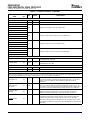
The C64x+ Central Processing Unit (CPU) consists of eight functional units, two register files, and two
data paths as shown in Figure 2-1 . The two general-purpose register files (A and B) each contain
thirty-two 32 bit registers for a total of 64 registers. The general-purpose registers can be used for data or
can be data address pointers. The data types supported include packed 8 bit data, packed 16 bit data, 32
bit data, 40 bit data, and 64 bit data. Values larger than 32 bits, such as 40 bit-long or 64 bit-long values
are stored in register pairs, with the 32 LSBs of data placed in an even register and the remaining 8 or
32 MSBs in the next upper register (which is always an odd-numbered register).
The eight functional units (.M1, .L1, .D1, .S1, .M2, .L2, .D2, and .S2) are each capable of executing one
instruction every clock cycle. The .M functional units perform all multiply operations. The .S and .L units
perform a general set of arithmetic, logical, and branch functions. The .D units primarily load data from
memory to the register file and store results from the register file into memory.
The C64x+ CPU extends the performance of the C64x core through enhancements and new features.
Each C64x+ .M unit can perform one of the following each clock cycle: one 32 x 32 bit multiply, two
16 x 16 bit multiplies, two 16 x 32 bit multiplies, four 8 x 8 bit multiplies, four 8 x 8 bit multiplies with add
operations, and four 16 x 16 multiplies with add/subtract capabilities (including a complex multiply). There
is also support for Galois field multiplication for 8 bit and 32 bit data. Many communications algorithms
such as FFTs and modems require complex multiplication. The complex multiply (CMPY) instruction takes
for 16 bit inputs and produces a 32 bit real and a 32 bit imaginary output. There are also complex
multiplies with rounding capability that produces one 32 bit packed output that contain 16 bit real and 16
bit imaginary values. The 32 x 32 bit multiply instructions provide the extended precision necessary for
audio and other high-precision algorithms on a variety of signed and unsigned 32 bit data types.
The .L or (Arithmetic Logic Unit) now incorporates the ability to do parallel add/subtract operations on a
pair of common inputs. Versions of this instruction exist to work on 32 bit data or on pairs of 16 bit data
performing dual 16 bit add and subtracts in parallel. There are also saturated forms of these instructions.
The C64x+ core enhances the .S unit in several ways. In the C64x core, dual 16 bit MIN2 and MAX2
comparisons were available only on the .L units. On the C64x+ core they also are available on the .S unit,
which increases the performance of algorithms that do searching and sorting. Finally, to increase data
packing and unpacking throughput, the .S unit allows sustained high performance for the quad 8 bit/16 bit
and dual 16 bit instructions. Unpack instructions prepare 8 bit data for parallel 16 bit operations. Pack
instructions return parallel results to output precision including saturation support.
Device Overview12 Submit Documentation Feedback

www.ti.com
SM320C6455-EP
FIXED-POINT DIGITAL SIGNAL PROCESSOR
SPRS462B – SEPTEMBER 2007 – REVISED JANUARY 2008
Other new features include:
• SPLOOP - A small instruction buffer in the CPU that aids in creation of software pipelining loops where
multiple iterations of a loop are executed in parallel. The SPLOOP buffer reduces the code size
associated with software pipelining. Furthermore, loops in the SPLOOP buffer are fully interruptible.
• Compact Instructions - The native instruction size for the C6000 devices is 32 bits. Many common
instructions such as MPY, AND, OR, ADD, and SUB can be expressed as 16 bits if the C64x+
compiler can restrict the code to use certain registers in the register file. This compression is
performed by the code generation tools.
• Instruction Set Enhancements - As noted above, there are new instructions such as 32 bit
multiplications, complex multiplications, packing, sorting, bit manipulation, and 32 bit Galois field
multiplication.
• Exception Handling - Intended to aid the programmer in isolating bugs. The C64x+ CPU is able to
detect and respond to exceptions, both from internally detected sources (such as illegal op-codes) and
from system events (such as a watchdog time expiration).
• Privilege - Defines user and supervisor modes of operation, allowing the operating system to give
a basic level of protection to sensitive resources. Local memory is divided into multiple pages, each
with read, write, and execute permissions.
• Time-Stamp Counter - Primarily targeted for Real-Time Operating System (RTOS) robustness, a
free-running time-stamp counter is implemented in the CPU which is not sensitive to system stalls.
For more details on the C64x+ CPU and its enhancements over the C64x architecture, see the following
documents:
• TMS320C64x/C64x+ DSP CPU and Instruction Set Reference Guide (literature number SPRU732 )
• TMS320C64x+ DSP Cache User's Guide (literature number SPRU862 )
• TMS320C64x+ Megamodule Reference Guide (literature number SPRU871 )
• TMS320C6455 Technical Reference (literature number SPRU965 )
• TMS320C64x to TMS320C64x+ CPU Migration Guide (literature number SPRAA84 )
Submit Documentation Feedback Device Overview 13

www.ti.com
src2
src2
.D1
.M1
.S1
.L1
long src
odd dst
src2
src1
src1
src1
src1
even dst
even dst
odd dst
dst1
dst
src2
src2
src2
long src
DA1
ST1b
LD1b
LD1a
ST1a
Data path A
Odd
register
file A
(A1, A3,
A5...A31)
Odd
register
file B
(B1, B3,
B5...B31)
.D2
src1
dst
src2
DA2
LD2a
LD2b
src2
.M2
src1
dst1
.S2
src1
even dst
long src
odd dst
ST2a
ST2b
long src
.L2
even dst
odd dst
src1
Data path B
Control Register
32 MSB
32 LSB
dst2
(A)
32 MSB
32 LSB
2x
1x
32 LSB
32 MSB
32 LSB
32 MSB
dst2
(B)
(B)
(A)
8
8
8
8
32
32
32
32
(C)
(C)
Even
register
file A
(A0, A2,
A4...A30)
Even
register
file B
(B0, B2,
B4...B30)
(D)
(D)
(D)
(D)
A. On .M unit, dst2 is 32 MSB.
B. On .M unit, dst1 is 32 LSB.
C. On C64x CPU .M unit, src2 is 32 bits; on C64x+ CPU .M unit, src2 is 64 bits.
D. On .L and .S units, odd dst connects to odd register files and even dst connects to even register files.
SM320C6455-EP
FIXED-POINT DIGITAL SIGNAL PROCESSOR
SPRS462B – SEPTEMBER 2007 – REVISED JANUARY 2008
Figure 2-1. C64x+™ CPU (DSP Core) Data Paths
Device Overview14 Submit Documentation Feedback

www.ti.com
2.3 Memory Map Summary
SM320C6455-EP
FIXED-POINT DIGITAL SIGNAL PROCESSOR
SPRS462B – SEPTEMBER 2007 – REVISED JANUARY 2008
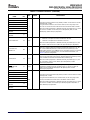
Table 2-2 shows the memory map address ranges of the C6455 device. The external memory
configuration register address ranges in the C6455 device begin at the hex address location 0x7000 0000
for EMIFA and hex address location 0x7800 0000 for DDR2 Memory Controller.
Table 2-2. C6455 Memory Map Summary
MEMORY BLOCK DESCRIPTION BLOCK SIZE (BYTES) HEX ADDRESS RANGE
Reserved 1024K 0000 0000 - 000F FFFF
Internal ROM 32K 0010 0000 - 0010 7FFF
Reserved 7M - 32K 0010 8000 - 007F FFFF
Internal RAM (L2) [L2 SRAM] 2M 0080 0000 - 009F FFFF
Reserved 4M 00A0 0000 - 00DF FFFF
L1P SRAM 32K 00E0 0000 - 00E0 7FFF
Reserved 1M - 32K 00E0 8000 - 00EF FFFF
L1D SRAM 32K 00F0 0000 - 00F0 7FFF
Reserved 1M - 32K 00F0 8000 - 00FF FFFF
Reserved 8M 0100 0000 - 017F FFFF
C64x+ Megamodule Registers 4M 0180 0000 - 01BF FFFF
Reserved 12.5M 01C0 0000 - 0287 FFFF
HPI Control Registers 256K 0288 0000 - 028B FFFF
McBSP 0 Registers 256K 028C 0000 - 028F FFFF
McBSP 1 Registers 256K 0290 0000 - 0293 FFFF
Timer 0 Registers 256K 0294 0000 - 0297 FFFF
Timer 1 Registers 128K 0298 0000 - 0299 FFFF
PLL1 Controller (including Reset Controller) Registers 512 029A 0000 - 029A 01FF
Reserved 256K - 512 029A 0200 - 029B FFFF
PLL2 Controller Registers 512 029C 0000 - 029C 01FF
Reserved 64K 029C 0200 - 029C FFFF
EDMA3 Channel Controller Registers 32K 02A0 0000 - 02A0 7FFF
Reserved 96K 02A0 8000 - 02A1 FFFF
EDMA3 Transfer Controller 0 Registers 32K 02A2 0000 - 02A2 7FFF
EDMA3 Transfer Controller 1 Registers 32K 02A2 8000 - 02A2 FFFF
EDMA3 Transfer Controller 2 Registers 32K 02A3 0000 - 02A3 7FFF
EDMA3 Transfer Controller 3 Registers 32K 02A3 8000 - 02A3 FFFF
Reserved 256K 02A4 0000 - 02A7 FFFF
Chip-Level Registers 256K 02A8 0000 - 02AB FFFF
Device State Control Registers 256K 02AC 0000 - 02AF FFFF
GPIO Registers 16K 02B0 0000 - 02B0 3FFF
I2C Data and Control Registers 256K 02B0 4000 - 02B3 FFFF
UTOPIA Control Registers 512 02B4 0000 - 02B4 01FF
Reserved 256K - 512 02B4 0200 - 02B7 FFFF
VCP2 Control Registers 128K 02B8 0000 - 02B9 FFFF
TCP2 Control Registers 128K 02BA 0000 - 02BB FFFF
Reserved 256K 02BC 0000 - 02BF FFFF
PCI Control Registers 256K 02C0 0000 - 02C3 FFFF
Reserved 256K 02C4 0000 - 02C7 FFFF
EMAC Control 4K 02C8 0000 - 02C8 0FFF
EMAC Control Module Registers 2K 02C8 1000 - 02C8 17FF
MDIO Control Registers 2K 02C8 1800 - 02C8 1FFF
Submit Documentation Feedback Device Overview 15

www.ti.com
SM320C6455-EP
FIXED-POINT DIGITAL SIGNAL PROCESSOR
SPRS462B – SEPTEMBER 2007 – REVISED JANUARY 2008
Table 2-2. C6455 Memory Map Summary (continued)
MEMORY BLOCK DESCRIPTION BLOCK SIZE (BYTES) HEX ADDRESS RANGE
EMAC Descriptor Memory 8K 02C8 2000 - 02C8 3FFF
Reserved 496K 02C8 4000 - 02CF FFFF
RapidIO Control Registers 256K 02D0 0000 - 02D3 FFFF
Reserved 768K 02D4 0000 - 02DF FFFF
RapidIO CPPI RAM 16K 02E0 0000 - 02E0 3FFF
Reserved 2M - 16K 02E0 4000 - 02FF FFFF
Reserved 16M 0300 0000 - 03FF FFFF
Reserved 192M 0400 0000 - 0FFF FFFF
Reserved 256M 1000 0000 - 1FFF FFFF
Reserved 256M 2000 0000 - 2FFF FFFF
McBSP 0 Data 256 3000 0000 - 3000 00FF
Reserved 64M - 256 3000 0100 - 33FF FFFF
McBSP 1 Data 256 3400 0000 - 3400 00FF
Reserved 64M - 256 3400 0100 - 37FF FFFF
UTOPIA Receive (Rx) Data Queue 1K 3C00 0000 - 3C00 03FF
UTOPIA Transmit (Tx) Data Queue 1K 3C00 0400 - 3C00 07FF
Reserved 16M - 2K 3C00 0800 - 3CFF FFFF
Reserved 48M 3D00 0000 - 3FFF FFFF
PCI External Memory Space 256M 4000 0000 - 4FFF FFFF
TCP2 Data Registers 128M 5000 0000 - 57FF FFFF
VCP2 Data Registers 128M 5800 0000 - 5FFF FFFF
Reserved 256M 6000 0000 - 6FFF FFFF
EMIFA (EMIF64) Configuration Registers 128M 7000 0000 - 77FF FFFF
DDR2 Memory Controller Configuration Registers 128M 7800 0000 - 7FFF FFFF
Reserved 256M 8000 0000 - 8FFF FFFF
Reserved 256M 9000 0000 - 9FFF FFFF
EMIFA CE2 - SBSRAM/Async
(1)
8M A000 0000 - A07F FFFF
Reserved 256M - 8M A080 0000 - AFFF FFFF
EMIFA CE3 - SBSRAM/Async
(1)
8M B000 0000 - B07F FFFF
Reserved 256M - 8M B080 0000 - BFFF FFFF
EMIFA CE4 - SBSRAM/Async
(1)
8M C000 0000 - C07F FFFF
Reserved 256M - 8M C080 0000 - CFFF FFFF
EMIFA CE5 - SBSRAM/Async
(1)
8M D000 0000 - D07F FFFF
Reserved 256M - 8M D080 0000 - DFFF FFFF
DDR2 Memory Controller CE0 - DDR2 SDRAM 512M E000 0000 - FFFF FFFF
(1) The EMIFA CE0 and CE1 are not functionally supported on the C6455 device, and therefore, are not pinned out.
Device Overview16 Submit Documentation Feedback

www.ti.com
2.4 Boot Sequence
2.4.1 Boot Modes Supported
SM320C6455-EP
FIXED-POINT DIGITAL SIGNAL PROCESSOR
SPRS462B – SEPTEMBER 2007 – REVISED JANUARY 2008
The boot sequence is a process by which the DSP's internal memory is loaded with program and data
sections and the DSP's internal registers are programmed with predetermined values. The boot sequence
is started automatically after each power-on reset, warm reset, max reset, and system reset. For more
details on the initiators of these resets, see Section 7.6 , Reset Controller.
There are several methods by which the memory and register initialization can take place. Each of these
methods is referred to as a boot mode. The boot mode to be used is selected at reset through the
BOOTMODE[3:0] pins.
Each boot mode can be classified as a hardware boot mode or as a software boot mode. Software boot
modes require the use of the on-chip bootloader. The bootloader is DSP code that transfers application
code from an external source into internal or external program memory after the DSP is taken out of reset.
The bootloader is permanently stored in the internal ROM of the DSP starting at byte address 0010
0000h. Hardware boot modes are carried out by the boot configuration logic. The boot configuration logic
is actual hardware that does not require the execution of DSP code. Section 2.4.1 , Boot Modes
Supported, describes each boot mode in more detail.
When accessing the internal ROM of the DSP, the CPU frequency must always be less than 750 MHz.
Therefore, when using a software boot mode, care must be taken such that the CPU frequency does not
exceed 750 MHz at any point during the boot sequence. After the boot sequence has completed, the CPU
frequency can be programmed to the frequency required by the application.
The C6455 has six boot modes:
• No boot (BOOTMODE[3:0] = 0000b)
With no boot, the CPU executes directly from the internal L2 SRAM located at address 0x80 0000.
Note: device operations are undefined if invalid code is located at address 0x80 0000. This boot mode
is a hardware boot mode.
• Host boot (BOOTMODE[3:0] = 0001b and BOOTMODE[3:0] = 0111b)
If host boot is selected, after reset, the CPU is internally "stalled" while the remainder of the device is
released. During this period, an external host can initialize the CPU's memory space as necessary
through Host Port Interface (HPI) or the Peripheral Component Interconnect (PCI) interface. Internal
configuration registers, such as those that control the EMIF also can be initialized by the host with two
exceptions: Device State Control registers (Section 3.4 ), PLL1 and PLL2 Controller registers
(Section 7.7 and Section 7.8 ) cannot be accessed through any host interface, including HPI and PCI.
Once the host is finished with all necessary initialization, it must generate a DSP interrupt (DSPINT) to
complete the boot process. This transition causes boot configuration logic to bring the CPU out of the
"stalled" state. The CPU then begins execution from the internal L2 SRAM located at 0x80 0000. Note
that the DSP interrupt is registered in bit 0 (channel 0) of the EDMA Event Register (ER). This event
must be cleared by software before triggering transfers on DMA channel 0.
All memory, with the exceptions previously described, may be written to and read by the host. This
allows for the host to verify what it sends to the DSP if required. After the CPU is out of the "stalled"
state, the CPU needs to clear the DSPINT, otherwise, no more DSPINTs can be received.
As previously mentioned, for the C6455 device, the Host Port Interface (HPI) and the Peripheral
Component Interconnect (PCI) interface can be used for host boot. To use the HPI for host boot, the
PCI_EN pin (Y29) must be low [default] (enabling the HPI peripheral) and BOOTMODE[3:0] must be
set to 0001b at device reset. Conversely, to use the PCI interface for host boot, the PCI_EN pin (Y29)
must be high (enabling the PCI peripheral) and BOOTMODE[3:0] must be set to 0111b at device reset.
For the HPI host boot, the DSP interrupt can be generated through the use of the DSPINT bit in the
HPI Control (HPIC) register.
For the HPI host boot, the CPU is actually held in reset until a DSP interrupt is generated by the host.
The DSP interrupt can be generated through the use of the DSPINT bit in the HPI Control (HPIC)
register. Because the CPU is held in reset during HPI host boot, it does not respond to emulation
Submit Documentation Feedback Device Overview 17

www.ti.com
SM320C6455-EP
FIXED-POINT DIGITAL SIGNAL PROCESSOR
SPRS462B – SEPTEMBER 2007 – REVISED JANUARY 2008
software such as Code Composer Studio.
For the PCI host boot, the CPU is out of reset, but it executes an IDLE instruction until a DSP interrupt
is generated by the host. The host can generate a DSP interrupt through the PCI peripheral by setting
the DSPINT bit in the Back-End Application Interrupt Enable Set Register (PCIBINTSET) and the
Status Set Register (PCISTATSET).
Note that the HPI host boot is a hardware boot mode while the PCI host boot is a software boot mode.
If PCI boot is selected, the on-chip bootloader configures the PLL1 Controller such that CLKIN1 is
multiplied by 15. More specifically, PLLM is set to 0Eh (x15) and RATIO is set to 0 ( ÷ 1) in the PLL1
Multiplier Control Register (PLLM) and PLL1 Pre-Divider Register (PREDIV), respectively. The CLKIN1
frequency must not be greater than 50 MHz so that the maximum speed of the internal ROM, 750
MHz, is not violated. The CFGGP[2:0] pins must be set to 000b during reset for proper operation of the
PCI boot mode.
As mentioned previously, a DSP interrupt must be generated at the end of the host boot process to
begin execution of the loaded application. Because the DSP interrupt generated by the HPI and PCI is
mapped to the EDMA event DSP_EVT (DMA channel 0), it will get recorded in bit 0 of the EDMA
Event Register (ER). This event must be cleared by software before triggering transfers on DMA
channel 0.
• EMIFA 8 bit ROM boot (BOOTMODE[3:0] = 0100b)
After reset, the device will begin executing software out of an Asynchronous 8 bit ROM located in
EMIFA CE3 space using the default settings in the EMIFA registers. This boot mode is a hardware
boot mode.
• Master I2C boot (BOOTMODE[3:0] = 0101b)
After reset, the DSP can act as a master to the I2C bus and copy data from an I2C EEPROM or a
device acting as an I2C slave to the DSP using a predefined boot table format. The destination
address and length are contained within the boot table. This boot mode is a software boot mode.
• Slave I2C boot (BOOTMODE[3:0] = 0110b)
A Slave I2C boot is also implemented, which programs the DSP as an I2C Slave and simply waits for a
Master to send data using a standard boot table format.
Using the Slave I2C boot, a single DSP or a device acting as an I2C Master can simultaneously boot
multiple slave DSPs connected to the same I2C bus. Note that the Master DSP may require booting
via an I2C EEPROM before acting as a Master and booting other DSPs.
The Slave I2C boot is a software boot mode.
• Serial RapidIO boot (BOOTMODE[3:0] = 1000b through 1111b)
After reset, the following sequence of events occur:
– The on-chip bootloader configures device registers, including SerDes, and EDMA3
– The on-chip bootloader resets the peripheral's state machines and registers
– RapidIO ports send idle control symbols to initialize SerDes ports
– The host explores the system with RapidIO maintenance packets
– The host identifies, enumerates, and initializes the RapidIO device
– The host controller configures DSP peripherals through maintenance packets
– The application software is sent from the host controller to DSP memory
– The DSP CPU is awakened by interrupt such as a RapidIO DOORBELL packet
– The application software is executed and normal operation follows
For Serial RapidIO boot, BOOTMODE2 (L26 pin) is used in conjunction with CFGGP[2:0] (T26, U26,
and U25 pins, respectively) to determine the device address within the RapidIO network.
BOOTMODE2 is the MSB of the address, while CFGGP[2:0] are used as the three LSBs–giving the
user the opportunity to have up to 16 unique device IDs.
BOOTMODE[1:0] (L25 and P26, respectively) denote the configuration of the RapidIO peripheral; i.e.,
"00b" refers to RapidIO Configuration 0. For exact device RapidIO Configurations, see the
TMS320C645xx Bootloader User's Guide (literature number SPRUEC6 ).
Device Overview18 Submit Documentation Feedback

www.ti.com
2.4.2 2nd-Level Bootloaders
SM320C6455-EP
FIXED-POINT DIGITAL SIGNAL PROCESSOR
SPRS462B – SEPTEMBER 2007 – REVISED JANUARY 2008
The SRIO boot is a software boot mode.
Any of the boot modes can be used to download a 2nd-level bootloader. A 2nd-level bootloader allows for
any level of customization to current boot methods as well as definition of a completely customized boot.
TI offers a few second-level bootloaders, such as an EMAC bootloader and a UTOPIA bootloader, which
can be loaded using the Master I2C boot.
Submit Documentation Feedback Device Overview 19

www.ti.com
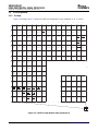
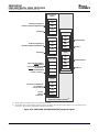
2.5 Pin Assignments
2.5.1 Pin Map
AG
AF
AE
AD
AC
AB
AA
Y
W
V
U
T
R
13121110987654321
13121110987654321
CLKR1/
GP[0]
HD15/
AD15
HD2/
AD2
URADDR0/
PGNT/
GP[12]
HD22/
AD22
DV
DD33
RSV15
UXADDR1/
PIDSEL
RSV16
HDS1/
PSERR
HINT/
PFRAME
DV
DD33
HHWIL/
PCLK
V
SS
HD12/
AD12
HD24/
AD24
RSV03
HD20/
AD20
HD18/
AD18
HD6/
AD6
HD16/
AD16
V
SS
HD28/
AD28
HD17/
AD17
HD31/
AD31
HD14/
AD14
HCNTL1/
PDEVSEL
HR/W/
PCBE2
HRDY/
PIRDY
URADDR1/
PRST/
GP[13]
HD21/
AD21
DV
DD33
V
SS
EMU8
RSV36
EMU11
EMU1
EMU10
EMU12
RSV37
EMU15
EMU4
EMU13
DV
DD33
DV
DD33
V
SS
EMU0
V
SS
DV
DD33
RSV38EMU6
CLKX1/
GP[3]
DV
DD33
V
SS
EMU18
DV
DD33
EMU5
V
SS
DV
DD33
HD9/
AD9
HD23/
AD23
HD3/
AD3
HD10/
AD10
GP[6]
V
SS
EMU14
GP[7]
RSV02
HD4/
AD4
HD30/
AD30
CV
DD
HD27/
AD27
V
SS
V
SS
V
SS
DV
DD33
V
SS
CV
DD
CV
DD
V
SS
DV
DD33
DV
DD33
V
SS
V
SS
DV
DD33
V
SS
V
SS
HD19/
AD19
HD13/
AD13
HD29/
AD29
DV
DD33
DV
DD33
HD25/
AD25
DV
DD33
HD0/
AD0
V
SS
HD11/
AD11
TOUTL0
EMU3
EMU7
TOUTL1
V
SS
DV
DD33
V
SS
DV
DD33
V
SS
HDS2/
PCBE1
HCNTL0/
PSTOP
HCS/
PPERR
V
SS
HD8/
AD8
V
SS
HD26/
AD26
V
SS
HD7/
AD7
HD1/
AD1
EMU2 RSV39
V
SS
DV
DD33
HAS/
PPAR
HD5/
AD5
AH
TINPL0 EMU17TDONMI EMU16GP[4]V
SS
TRST
TDI
RSV27 EMU9
AJ
TINPL1 TMSV
SS
CLKS RSV40
GP[5]DV
DD33
DV
DD33
TCK
RSV26
SYSCLK4/
GP[1]
14
V
SS
DV
DD33
RESETSTAT
POR
V
SS
CV
DD
CV
DD
RESET
DV
DD33
V
SS
15
AV
DDA
V
SS
DV
DD33
RIOCLK
CV
DD
V
SS
V
SS
RIOCLK
V
SS
DV
DD33
14 15
V
SS
CV
DD
CV
DD
CV
DD
V
SS
V
SS
V
SS
CV
DD
DV
DDRM
V
SS
V
SS
CV
DD
AG
AF
AE
AD
AC
AB
AA
Y
W
V
U
T
R
AH
AJFSX0 DR0
FSR0
DR1/
GP[8]
CLKR0
FSX1/
GP[11]
DX1/
GP[9]
CLKX0
DX0
FSR1/
GP[10]
SM320C6455-EP
FIXED-POINT DIGITAL SIGNAL PROCESSOR
SPRS462B – SEPTEMBER 2007 – REVISED JANUARY 2008
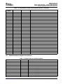
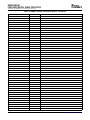
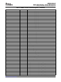
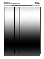
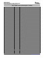
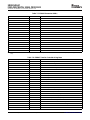
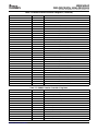
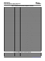
Figure 2-2 through Figure 2-5 show the C6455 pin assignments in four quadrants (A, B, C, and D).
Figure 2-2. C6455 Pin Map (Bottom View) [Quadrant A]
Device Overview20 Submit Documentation Feedback
Page is loading ...
Page is loading ...
Page is loading ...
Page is loading ...
Page is loading ...
Page is loading ...
Page is loading ...
Page is loading ...
Page is loading ...
Page is loading ...
Page is loading ...
Page is loading ...
Page is loading ...
Page is loading ...
Page is loading ...
Page is loading ...
Page is loading ...
Page is loading ...
Page is loading ...
Page is loading ...
Page is loading ...
Page is loading ...
Page is loading ...
Page is loading ...
Page is loading ...
Page is loading ...
Page is loading ...
Page is loading ...
Page is loading ...
Page is loading ...
Page is loading ...
Page is loading ...
Page is loading ...
Page is loading ...
Page is loading ...
Page is loading ...
Page is loading ...
Page is loading ...
Page is loading ...
Page is loading ...
Page is loading ...
Page is loading ...
Page is loading ...
Page is loading ...
Page is loading ...
Page is loading ...
Page is loading ...
Page is loading ...
Page is loading ...
Page is loading ...
Page is loading ...
Page is loading ...
Page is loading ...
Page is loading ...
Page is loading ...
Page is loading ...
Page is loading ...
Page is loading ...
Page is loading ...
Page is loading ...
Page is loading ...
Page is loading ...
Page is loading ...
Page is loading ...
Page is loading ...
Page is loading ...
Page is loading ...
Page is loading ...
Page is loading ...
Page is loading ...
Page is loading ...
Page is loading ...
Page is loading ...
Page is loading ...
Page is loading ...
Page is loading ...
Page is loading ...
Page is loading ...
Page is loading ...
Page is loading ...
Page is loading ...
Page is loading ...
Page is loading ...
Page is loading ...
Page is loading ...
Page is loading ...
Page is loading ...
Page is loading ...
Page is loading ...
Page is loading ...
Page is loading ...
Page is loading ...
Page is loading ...
Page is loading ...
Page is loading ...
Page is loading ...
Page is loading ...
Page is loading ...
Page is loading ...
Page is loading ...
Page is loading ...
Page is loading ...
Page is loading ...
Page is loading ...
Page is loading ...
Page is loading ...
Page is loading ...
Page is loading ...
Page is loading ...
Page is loading ...
Page is loading ...
Page is loading ...
Page is loading ...
Page is loading ...
Page is loading ...
Page is loading ...
Page is loading ...
Page is loading ...
Page is loading ...
Page is loading ...
Page is loading ...
Page is loading ...
Page is loading ...
Page is loading ...
Page is loading ...
Page is loading ...
Page is loading ...
Page is loading ...
Page is loading ...
Page is loading ...
Page is loading ...
Page is loading ...
Page is loading ...
Page is loading ...
Page is loading ...
Page is loading ...
Page is loading ...
Page is loading ...
Page is loading ...
Page is loading ...
Page is loading ...
Page is loading ...
Page is loading ...
Page is loading ...
Page is loading ...
Page is loading ...
Page is loading ...
Page is loading ...
Page is loading ...
Page is loading ...
Page is loading ...
Page is loading ...
Page is loading ...
Page is loading ...
Page is loading ...
Page is loading ...
Page is loading ...
Page is loading ...
Page is loading ...
Page is loading ...
Page is loading ...
Page is loading ...
Page is loading ...
Page is loading ...
Page is loading ...
Page is loading ...
Page is loading ...
Page is loading ...
Page is loading ...
Page is loading ...
Page is loading ...
Page is loading ...
Page is loading ...
Page is loading ...
Page is loading ...
Page is loading ...
Page is loading ...
Page is loading ...
Page is loading ...
Page is loading ...
Page is loading ...
Page is loading ...
Page is loading ...
Page is loading ...
Page is loading ...
Page is loading ...
Page is loading ...
Page is loading ...
Page is loading ...
Page is loading ...
Page is loading ...
Page is loading ...
Page is loading ...
Page is loading ...
Page is loading ...
Page is loading ...
Page is loading ...
Page is loading ...
Page is loading ...
Page is loading ...
Page is loading ...
Page is loading ...
Page is loading ...
Page is loading ...
Page is loading ...
Page is loading ...
Page is loading ...
Page is loading ...
Page is loading ...
Page is loading ...
Page is loading ...
Page is loading ...
Page is loading ...
Page is loading ...
Page is loading ...
Page is loading ...
Page is loading ...
Page is loading ...
Page is loading ...
Page is loading ...
Page is loading ...
Page is loading ...
Page is loading ...
Page is loading ...
Page is loading ...
Page is loading ...
Page is loading ...
Page is loading ...
Page is loading ...
Page is loading ...
Page is loading ...
Page is loading ...
Page is loading ...
Page is loading ...
-
 1
1
-
 2
2
-
 3
3
-
 4
4
-
 5
5
-
 6
6
-
 7
7
-
 8
8
-
 9
9
-
 10
10
-
 11
11
-
 12
12
-
 13
13
-
 14
14
-
 15
15
-
 16
16
-
 17
17
-
 18
18
-
 19
19
-
 20
20
-
 21
21
-
 22
22
-
 23
23
-
 24
24
-
 25
25
-
 26
26
-
 27
27
-
 28
28
-
 29
29
-
 30
30
-
 31
31
-
 32
32
-
 33
33
-
 34
34
-
 35
35
-
 36
36
-
 37
37
-
 38
38
-
 39
39
-
 40
40
-
 41
41
-
 42
42
-
 43
43
-
 44
44
-
 45
45
-
 46
46
-
 47
47
-
 48
48
-
 49
49
-
 50
50
-
 51
51
-
 52
52
-
 53
53
-
 54
54
-
 55
55
-
 56
56
-
 57
57
-
 58
58
-
 59
59
-
 60
60
-
 61
61
-
 62
62
-
 63
63
-
 64
64
-
 65
65
-
 66
66
-
 67
67
-
 68
68
-
 69
69
-
 70
70
-
 71
71
-
 72
72
-
 73
73
-
 74
74
-
 75
75
-
 76
76
-
 77
77
-
 78
78
-
 79
79
-
 80
80
-
 81
81
-
 82
82
-
 83
83
-
 84
84
-
 85
85
-
 86
86
-
 87
87
-
 88
88
-
 89
89
-
 90
90
-
 91
91
-
 92
92
-
 93
93
-
 94
94
-
 95
95
-
 96
96
-
 97
97
-
 98
98
-
 99
99
-
 100
100
-
 101
101
-
 102
102
-
 103
103
-
 104
104
-
 105
105
-
 106
106
-
 107
107
-
 108
108
-
 109
109
-
 110
110
-
 111
111
-
 112
112
-
 113
113
-
 114
114
-
 115
115
-
 116
116
-
 117
117
-
 118
118
-
 119
119
-
 120
120
-
 121
121
-
 122
122
-
 123
123
-
 124
124
-
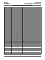 125
125
-
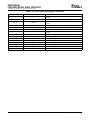 126
126
-
 127
127
-
 128
128
-
 129
129
-
 130
130
-
 131
131
-
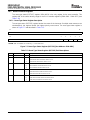 132
132
-
 133
133
-
 134
134
-
 135
135
-
 136
136
-
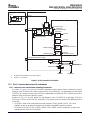 137
137
-
 138
138
-
 139
139
-
 140
140
-
 141
141
-
 142
142
-
 143
143
-
 144
144
-
 145
145
-
 146
146
-
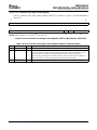 147
147
-
 148
148
-
 149
149
-
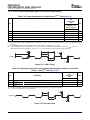 150
150
-
 151
151
-
 152
152
-
 153
153
-
 154
154
-
 155
155
-
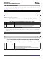 156
156
-
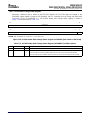 157
157
-
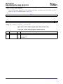 158
158
-
 159
159
-
 160
160
-
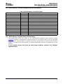 161
161
-
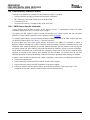 162
162
-
 163
163
-
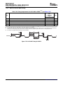 164
164
-
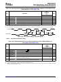 165
165
-
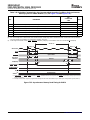 166
166
-
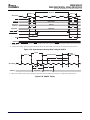 167
167
-
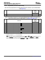 168
168
-
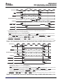 169
169
-
 170
170
-
 171
171
-
 172
172
-
 173
173
-
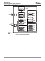 174
174
-
 175
175
-
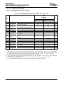 176
176
-
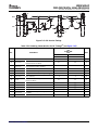 177
177
-
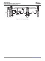 178
178
-
 179
179
-
 180
180
-
 181
181
-
 182
182
-
 183
183
-
 184
184
-
 185
185
-
 186
186
-
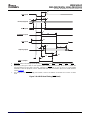 187
187
-
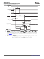 188
188
-
 189
189
-
 190
190
-
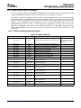 191
191
-
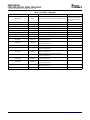 192
192
-
 193
193
-
 194
194
-
 195
195
-
 196
196
-
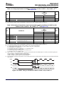 197
197
-
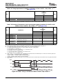 198
198
-
 199
199
-
 200
200
-
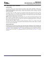 201
201
-
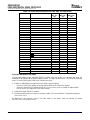 202
202
-
 203
203
-
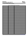 204
204
-
 205
205
-
 206
206
-
 207
207
-
 208
208
-
 209
209
-
 210
210
-
 211
211
-
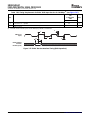 212
212
-
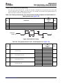 213
213
-
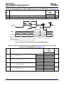 214
214
-
 215
215
-
 216
216
-
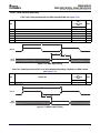 217
217
-
 218
218
-
 219
219
-
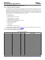 220
220
-
 221
221
-
 222
222
-
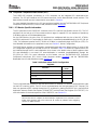 223
223
-
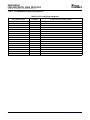 224
224
-
 225
225
-
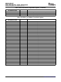 226
226
-
 227
227
-
 228
228
-
 229
229
-
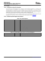 230
230
-
 231
231
-
 232
232
-
 233
233
-
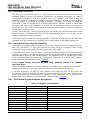 234
234
-
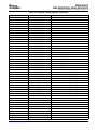 235
235
-
 236
236
-
 237
237
-
 238
238
-
 239
239
-
 240
240
-
 241
241
-
 242
242
-
 243
243
-
 244
244
-
 245
245
-
 246
246
-
 247
247
-
 248
248
-
 249
249
-
 250
250
-
 251
251
-
 252
252
-
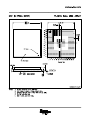 253
253
-
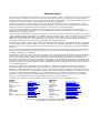 254
254


Texas Instruments SM320C6455-EP User manual
- Category
- Motherboards
- Type
- User manual
Ask a question and I''ll find the answer in the document
Finding information in a document is now easier with AI
Related papers
-
Texas Instruments TMS320DM643X DMP User manual
-
-
-
-
-
-
-
-
-
Other documents
-
Apple USB 2.0 User manual
-
Intel 82544GC/EI User manual
-
-
AMP FSR1 Quick start guide
-
Emac NGRIPVNE Installation guide
-
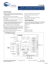 Cypress EZ-Host CY7C67300 User manual
-
Marquant MCR-1254 Datasheet
-
 Crux Interfacing Solutions CRXi 122801 User manual
-
Utopia Alley CR2BK Operating instructions
-
Maxim DS33Z41 User manual

