Page is loading ...

TMS3320C5515 DSP System
User's Guide
Literature Number: SPRUFX5A
October 2010–Revised November 2010


Contents
Preface ....................................................................................................................................... 9
1 System Control ................................................................................................................. 13
1.1 Introduction ................................................................................................................. 13
1.1.1 Block Diagram .................................................................................................... 13
1.1.2 CPU Core .......................................................................................................... 14
1.1.3 FFT Hardware Accelerator ...................................................................................... 14
1.1.4 Power Management .............................................................................................. 15
1.1.5 Peripherals ........................................................................................................ 15
1.2 System Memory ........................................................................................................... 16
1.2.1 Program/Data Memory Map ..................................................................................... 16
1.2.2 I/O Memory Map .................................................................................................. 20
1.3 Device Clocking ............................................................................................................ 20
1.3.1 Overview ........................................................................................................... 20
1.3.2 Clock Domains .................................................................................................... 23
1.4 System Clock Generator ................................................................................................. 23
1.4.1 Overview ........................................................................................................... 23
1.4.2 Functional Description ........................................................................................... 24
1.4.3 Configuration ...................................................................................................... 26
1.4.4 Clock Generator Registers ...................................................................................... 29
1.5 Power Management ....................................................................................................... 33
1.5.1 Overview ........................................................................................................... 33
1.5.2 Power Domains ................................................................................................... 33
1.5.3 Clock Management ............................................................................................... 34
1.5.4 Static Power Management ...................................................................................... 46
1.5.5 Power Configurations ............................................................................................ 50
1.6 Interrupts .................................................................................................................... 53
1.6.1 IFR and IER Registers ........................................................................................... 54
1.6.2 Interrupt Timing ................................................................................................... 55
1.6.3 Timer Interrupt Aggregation Flag Register (TIAFR) [1C14h] ............................................... 56
1.6.4 GPIO Interrupt Enable and Aggregation Flag Registers .................................................... 56
1.6.5 DMA Interrupt Enable and Aggregation Flag Registers ..................................................... 56
1.7 System Configuration and Control ...................................................................................... 57
1.7.1 Overview ........................................................................................................... 57
1.7.2 Device Identification .............................................................................................. 57
1.7.3 Device Configuration ............................................................................................. 61
1.7.4 DMA Controller Configuration ................................................................................... 70
1.7.5 Peripheral Reset .................................................................................................. 73
1.7.6 EMIF and USB Byte Access .................................................................................... 75
1.7.7 EMIF Clock Divider Register (ECDR) [1C26h] ............................................................... 77
3
SPRUFX5A–October 2010–Revised November 2010 Contents
Submit Documentation Feedback
Copyright © 2010, Texas Instruments Incorporated

www.ti.com
List of Figures
1-1. Functional Block Diagram ................................................................................................ 13
1-2. DSP Memory Map ........................................................................................................ 17
1-3. DSP Clocking Diagram .................................................................................................. 22
1-4. Clock Generator ........................................................................................................... 24
1-5. CLKOUT Control Source Select Register (CCSSR) [1C24h]........................................................ 25
1-6. Clock Generator Control Register 1 (CGCR1) [1C20h] .............................................................. 30
1-7. Clock Generator Control Register 2 (CGCR2) [1C21h] .............................................................. 30
1-8. Clock Generator Control Register 3 (CGCR3) [1C22h] .............................................................. 31
1-9. Clock Generator Control Register 4 (CGCR4) [1C23h] .............................................................. 31
1-10. Clock Configuration Register 1 (CCR1) [1C1Eh]...................................................................... 32
1-11. Clock Configuration Register 2 (CCR2) [1C1Fh]...................................................................... 32
1-12. Idle Configuration Register (ICR) [0001h].............................................................................. 36
1-13. Idle Status Register (ISTR) [0002h]..................................................................................... 37
1-14. Peripheral Clock Gating Configuration Register 1 (PCGCR1) [1C02h] ............................................ 39
1-15. Peripheral Clock Gating Configuration Register 2 (PCGCR2) [1C03h] ............................................ 41
1-16. Peripheral Clock Stop Request/Acknowledge Register (CLKSTOP) [1C3Ah] .................................... 42
1-17. USB System Control Register (USBSCR) [1C32h] ................................................................... 44
1-18. RTC Power Management Register (RTCPMGT) [1930h]............................................................ 46
1-19. RTC Interrupt Flag Register (RTCINTFL) [1920h] .................................................................... 47
1-20. RAM Sleep Mode Control Register1 [0x1C28] ........................................................................ 48
1-21. RAM Sleep Mode Control Register2 [0x1C2A]........................................................................ 49
1-22. RAM Sleep Mode Control Register3 [0x1C2B]........................................................................ 49
1-23. RAM Sleep Mode Control Register4 [0x1C2C]........................................................................ 49
1-24. RAM Sleep Mode Control Register5 [0x1C2D]........................................................................ 49
1-25. IFR0 and IER0 Bit Locations............................................................................................. 54
1-26. IFR1 and IER1 Bit Locations............................................................................................. 55
1-27. Die ID Register 0 (DIEIDR0) [1C40h]................................................................................... 58
1-28. Die ID Register 1 (DIEIDR1) [1C41h]................................................................................... 58
1-29. Die ID Register 2 (DIEIDR2) [1C42h]................................................................................... 58
1-30. Die ID Register 3 (DIEIDR3[15:0]) [1C43h]............................................................................ 59
1-31. Die ID Register 4 (DIEIDR4) [1C44h]................................................................................... 59
1-32. Die ID Register 5 (DIEIDR5) [1C45h]................................................................................... 59
1-33. Die ID Register 6 (DIEIDR6) [1C46h]................................................................................... 60
1-34. Die ID Register 7 (DIEIDR7) [1C47h]................................................................................... 60
1-35. External Bus Selection Register (EBSR) [1C00h]..................................................................... 61
1-36. RTC Power Management Register (RTCPMGT) [1930h]............................................................ 63
1-37. LDO Control Register (LDOCNTL) [7004h]............................................................................ 65
1-38. Output Slew Rate Control Register (OSRCR) [1C16h]............................................................... 66
1-39. Pull-Down Inhibit Register 1 (PDINHIBR1) [1C17h] .................................................................. 67
1-40. Pull-Down Inhibit Register 2 (PDINHIBR2) [1C18h] .................................................................. 68
1-41. Pull-Down Inhibit Register 3 (PDINHIBR3) [1C19h] .................................................................. 69
1-42. DMA Interrupt Flag Register (DMAIFR) [1C30h]...................................................................... 72
1-43. DMA Interrupt Enable Register (DMAIER) [1C31h]................................................................... 72
1-44. DMAn Channel Event Source Register 1 (DMAnCESR1) [1C1Ah, 1C1Ch, 1C36h, and 1C38h] .............. 73
1-45. DMAn Channel Event Source Register 2 (DMAnCESR2) [1C1Bh, 1C1Dh, 1C37h, and 1C39h] .............. 73
1-46. Peripheral Software Reset Counter Register (PSRCR) [1C04h].................................................... 74
1-47. Peripheral Reset Control Register (PRCR) [1C05h].................................................................. 74
4
List of Figures SPRUFX5A–October 2010–Revised November 2010
Submit Documentation Feedback
Copyright © 2010, Texas Instruments Incorporated

www.ti.com
1-48. EMIF System Control Register (ESCR) [1C33h]...................................................................... 76
1-49. EMIF Clock Divider Register (ECDR) [1C26h] ........................................................................ 77
5
SPRUFX5A–October 2010–Revised November 2010 List of Figures
Submit Documentation Feedback
Copyright © 2010, Texas Instruments Incorporated

www.ti.com
List of Tables
1-1. ............................................................................................................................... 14
1-2. DARAM Blocks ............................................................................................................ 17
1-3. SARAM Blocks............................................................................................................. 18
1-4. SAROM Blocks ............................................................................................................ 19
1-5. PLL Output Frequency Configuration................................................................................... 24
1-6. CLKOUT Control Source Select Register (CCSSR) Field Descriptions............................................ 25
1-7. Clock Generator Control Register Bits Used In BYPASS MODE................................................... 27
1-8. Output Frequency in Bypass Mode ..................................................................................... 27
1-9. Clock Generator Control Register Bits Used In PLL Mode .......................................................... 27
1-10. PLL Clock Frequency Ranges........................................................................................... 28
1-11. Examples of Selecting a PLL MODE Frequency, When CLK_SEL=L ............................................. 29
1-12. Clock Generator Registers............................................................................................... 29
1-13. Clock Generator Control Register 1 (CGCR1) Field Descriptions .................................................. 30
1-14. Clock Generator Control Register 2 (CGCR2) Field Descriptions .................................................. 30
1-15. Clock Generator Control Register 3 (CGCR3) Field Descriptions .................................................. 31
1-16. Clock Generator Control Register 4 (CGCR4) Field Descriptions .................................................. 31
1-17. Clock Configuration Register 1 (CCR1) Field Descriptions.......................................................... 32
1-18. Clock Configuration Register 2 (CCR2) Field Descriptions.......................................................... 32
1-19. Power Management Features ........................................................................................... 33
1-20. DSP Power Domains...................................................................................................... 34
1-21. Idle Configuration Register (ICR) Field Descriptions ................................................................. 36
1-22. Idle Status Register (ISTR) Field Descriptions ........................................................................ 37
1-23. CPU Clock Domain Idle Requirements................................................................................. 37
1-24. Peripheral Clock Gating Configuration Register 1 (PCGCR1) Field Descriptions ................................ 39
1-25. Peripheral Clock Gating Configuration Register 2 (PCGCR2) Field Descriptions ................................ 41
1-26. Peripheral Clock Stop Request/Acknowledge Register (CLKSTOP) Field Descriptions......................... 42
1-27. USB System Control Register (USBSCR) Field Descriptions....................................................... 44
1-28. RTC Power Management Register (RTCPMGT) Field Descriptions ............................................... 46
1-29. RTC Interrupt Flag Register (RTCINTFL) Field Descriptions........................................................ 47
1-30. On-Chip Memory Standby Modes....................................................................................... 48
1-31. Power Configurations ..................................................................................................... 50
1-32. Interrupt Table ............................................................................................................. 53
1-33. IFR0 and IER0 Bit Descriptions ......................................................................................... 54
1-34. IFR1 and IER1 Bit Descriptions ......................................................................................... 55
1-35. Die ID Registers ........................................................................................................... 57
1-36. Die ID Register 0 (DIEIDR0) Field Descriptions....................................................................... 58
1-37. Die ID Register 1 (DIEIDR1) Field Descriptions....................................................................... 58
1-38. Die ID Register 2 (DIEIDR2) Field Descriptions....................................................................... 58
1-39. Die ID Register 3 (DIEIDR3[15:0]) Field Descriptions................................................................ 59
1-40. Die ID Register 4 (DIEIDR4) Field Descriptions....................................................................... 59
1-41. Die ID Register 5 (DIEIDR5) Field Descriptions....................................................................... 59
1-42. Die ID Register 6 (DIEIDR6) Field Descriptions....................................................................... 60
1-43. Die ID Register 7 (DIEIDR7) Field Descriptions....................................................................... 60
1-44. EBSR Register Bit Descriptions Field Descriptions................................................................... 62
1-45. RTCPMGT Register Bit Descriptions Field Descriptions............................................................. 64
1-46. LDOCNTL Register Bit Descriptions Field Descriptions.............................................................. 65
1-47. LDO Controls Matrix ...................................................................................................... 65
6
List of Tables SPRUFX5A–October 2010–Revised November 2010
Submit Documentation Feedback
Copyright © 2010, Texas Instruments Incorporated

www.ti.com
1-48. Output Slew Rate Control Register (OSRCR) Field Descriptions................................................... 66
1-49. Pull-Down Inhibit Register 1 (PDINHIBR1) Field Descriptions ...................................................... 67
1-50. Pull-Down Inhibit Register 2 (PDINHIBR2) Field Descriptions ...................................................... 68
1-51. Pull-Down Inhibit Register 3 (PDINHIBR3) Field Descriptions ...................................................... 69
1-52. Channel Synchronization Events for DMA Controllers ............................................................... 71
1-53. System Registers Related to the DMA Controllers ................................................................... 71
1-54. DMA Interrupt Flag Register (DMAIFR) Field Descriptions.......................................................... 72
1-55. DMA Interrupt Enable Register (DMAIER) Field Descriptions....................................................... 72
1-56. DMAn Channel Event Source Register 1 (DMAnCESR1) Field Descriptions..................................... 73
1-57. DMAn Channel Event Source Register 2 (DMAnCESR2) Field Descriptions..................................... 73
1-58. Peripheral Software Reset Counter Register (PSRCR) Field Descriptions........................................ 74
1-59. Peripheral Reset Control Register (PRCR) Field Descriptions...................................................... 74
1-60. Effect of BYTEMODE Bits on EMIF Accesses ........................................................................ 76
1-61. Effect of USBSCR BYTEMODE Bits on USB Access................................................................ 76
1-62. EMIF System Control Register (ESCR) Field Descriptions.......................................................... 76
1-63. EMIF Clock Divider Register (ECDR) Field Descriptions ............................................................ 77
7
SPRUFX5A–October 2010–Revised November 2010 List of Tables
Submit Documentation Feedback
Copyright © 2010, Texas Instruments Incorporated


Preface
SPRUFX5A–October 2010–Revised November 2010
Read This First
About This Manual
This document describes various aspects of the TMS320C5515 digital signal processor (DSP) including:
system memory, device clocking options and operation of the DSP clock generator, power management
features, interrupts, and system control.
Notational Conventions
This document uses the following conventions.
• Hexadecimal numbers are shown with the suffix h. For example, the following number is 40
hexadecimal (decimal 64): 40h.
• Registers in this document are shown in figures and described in tables.
– Each register figure shows a rectangle divided into fields that represent the fields of the register.
Each field is labeled with its bit name, its beginning and ending bit numbers above, and its
read/write properties below. A legend explains the notation used for the properties.
– Reserved bits in a register figure designate a bit that is used for future device expansion.
Related Documentation From Texas Instruments
The following documents describe the TMS320C5515/14/05/04 Digital Signal Processor (DSP) Digital
Signal Processor (DSP). Copies of these documents are available on the internet at http://www.ti.com.
SWPU073 — TMS320C55x 3.0 CPU Reference Guide. This manual describes the architecture,
registers, and operation of the fixed-point TMS320C55x digital signal processor (DSP) CPU.
SPRU652 — TMS320C55x DSP CPU Programmer’s Reference Supplement. This document describes
functional exceptions to the CPU behavior.
SPRUFO1A — TMS320C5515/14/05/04/VC05/VC04 Digital Signal Processor (DSP) Inter-Integrated
Circuit (I2C) Peripheral User's Guide. This document describes the inter-integrated circuit (I2C)
peripheral in the TMS320C5515/14/05/04/VC05/VC04 Digital Signal Processor (DSP) devices. The
I2C peripheral provides an interface between the device and other devices compliant with Phillips
Semiconductors Inter-IC bus (I2C-bus) specification version 2.1 and connected by way of an
I2C-bus. This document assumes the reader is familiar with the I2C-bus specification.
SPRUFO2 — TMS320C5515/14/05/04/VC05/VC04 Digital Signal Processor (DSP) Timer/Watchdog
Timer User's Guide. This document provides an overview of the three 32-bit timers in the
TMS320C5515/14/05/04/VC05/VC04 Digital Signal Processor (DSP) devices. The 32-bit timers of
the device are software programmable timers that can be configured as general-purpose (GP)
timers. Timer 2 can be configured as a GP, a Watchdog (WD), or both simultaneously.
SPRUFO3 — TMS320C5515/14/05/04/VC05/VC04 Digital Signal Processor (DSP) Serial Peripheral
Interface (SPI) User's Guide. This document describes the serial peripheral interface (SPI) in the
TMS320C5515/14/05/04/VC05/VC04 Digital Signal Processor (DSP) devices. The SPI is a
high-speed synchronous serial input/output port that allows a serial bit stream of programmed
length (1 to 32 bits) to be shifted into and out of the device at a programmed bit-transfer rate. The
SPI supports multi-chip operation of up to four SPI slave devices. The SPI can operate as a master
device only.
9
SPRUFX5A–October 2010–Revised November 2010 Read This First
Submit Documentation Feedback
Copyright © 2010, Texas Instruments Incorporated

Related Documentation From Texas Instruments
www.ti.com
SPRUFO4 — TMS320C5515/14/05/04/VC05/VC04 Digital Signal Processor (DSP) General-Purpose
Input/Output (GPIO) User's Guide. This document describes the general-purpose input/output
(GPIO) on the TMS320C5515/14/05/04/VC05/VC04 digital signal processor (DSP) devices. The
GPIO peripheral provides dedicated general-purpose pins that can be configured as either inputs or
outputs. When configured as an input, you can detect the state of an internal register. When
configured as an output you can write to an internal register to control the state driven on the output
pin.
SPRUFO5 — TMS320C5515/14/05/04/VC05/VC04 Digital Signal Processor (DSP) Universal
Asynchronous Receiver/Transmitter (UART) User's Guide. This document describes the
universal asynchronous receiver/transmitter (UART) peripheral in the
TMS320C5515/14/05/04/VC05/VC04 Digital Signal Processor (DSP) devices. The UART performs
serial-to-parallel conversions on data received from a peripheral device and parallel-to-serial
conversion on data received from the CPU.
SPRUFP1 — TMS320C5515/05/VC05 Digital Signal Processor (DSP) Successive Approximation
(SAR) Analog to Digital Converter (ADC) User's Guide. This document provides an overview of
the Successive Approximation (SAR) Analog to Digital Converter (ADC) on the
TMS320C5515/14/05/04/VC05/VC04 Digital Signal Processor (DSP) devices. The SAR is a 10-bit
ADC using a switched capacitor architecture which converts an analog input signal to a digital
value.
SPRUFP3 — TMS320C5515/05/VC05 Digital Signal Processor (DSP) Liquid Crystal Display
Controller (LCDC) User's Guide. This document describes the liquid crystal display controller
(LCDC) in the TMS320C5515/14/05/04/VC05/VC04 Digital Signal Processor (DSP) devices. The
LCD controller includes a LCD Interface Display Driver (LIDD) controller.
SPRUFT2— TMS320C5515/14/05/04 DSP Direct Memory Access (DMA) Controller User's Guide This
document describes the features and operation of the DMA controller that is available on the
TMS320C5515/14/05/04 Digital Signal Processor (DSP) devices. The DMA controller is used to
move data among internal memory, external memory, and peripherals without intervention from the
CPU and in the background of CPU operation.
SPRUGU6— TMS320C5515/14/05/04 DSP External Memory Interface (EMIF) User's Guide. This
document describes the operation of the external memory interface (EMIF) in the
TMS320C5515/14/05/04 Digital Signal Processor (DSP) devices. The purpose of the EMIF is to
provide a means to connect to a variety of external devices.
SPRUFO6— TMS320C5515/14/05/04/VC05/VC04 DSP Multimedia Card (MMC)/Secure Digital (SD)
Card Controller This document describes the Multimedia Card (MMC)/Secure Digital (SD) Card
Controller on the TMS320C5515/14/05/04 Digital Signal Processor (DSP) devices. The multimedia
card (MMC)/secure digital (SD) card is used in a number of applications to provide removable data
storage. The MMC/SD card controller provides an interface to external MMC and SD cards.
SPRUFX2— TMS320C5515/14/05/04 Digital Signal Processor (DSP) Real-Time Clock (RTC) User's
Guide.This document describes the operation of the Real-Time Clock (RTC) module in the
TMS320C5515/14/05/04 Digital Signal Processor (DSP) devices. The RTC also has the capability
to wake-up the power management and apply power to the rest of the device through an alarm,
periodic interrupt, or external WAKEUP signal.
SPRUFX4— TMS320C5515/14/05/04 Digital Signal Processor (DSP) Inter-IC Sound (I2S) Bus User's
Guide. This document describes the features and operation of Inter-IC Sound (I2S) Bus in the
TMS320C5515/14/05/04 Digital Signal Processor (DSP) devices. This peripheral allows serial
transfer of full duplex streaming data, usually streaming audio, between DSP and an external I2S
peripheral device such as an audio codec.
SPRUFX5— TMS320C5515 DSP System User's Guide. This document describes various aspects of the
TMS320C5515 digital signal processor (DSP) including: system memory, device clocking options
and operation of the DSP clock generator, power management features, interrupts, and system
control.
10
Read This First SPRUFX5A–October 2010–Revised November 2010
Submit Documentation Feedback
Copyright © 2010, Texas Instruments Incorporated

www.ti.com
Related Documentation From Texas Instruments
SPRUGH5— TMS320C5505 DSP System User's Guide. This document describes various aspects of
the TMS320C5505 digital signal processor (DSP) including: system memory, device clocking
options and operation of the DSP clock generator, power management features, interrupts, and
system control.
SPRUFX6— TMS320C5514 DSP System User's Guide. This document describes various aspects of the
TMS320C5514 digital signal processor (DSP) including: system memory, device clocking options
and operation of the DSP clock generator, power management features, interrupts, and system
control.
SPRUGH6— TMS320C5504 DSP System User's Guide.This document describes various aspects of the
TMS320C5504 digital signal processor (DSP) including: system memory, device clocking options
and operation of the DSP clock generator, power management features, interrupts, and system
control.
SPRUGH9— TMS320C5515 DSP Universal Serial Bus 2.0 (USB) Controller User's Guide This
document describes the universal serial bus 2.0 (USB) in the TMS320C5515 Digital Signal
Processor (DSP) devices. The USB controller supports data throughput rates up to 480 Mbps. It
provides a mechanism for data transfer between USB devices.
SPRABB6— FFT Implementation on the TMS320VC5505, TMS320C5505, and TMS320C5515 DSPs
This document describes FFT computation on the TMS320VC5505 and TMS320C5505/15 DSPs
devices.
11
SPRUFX5A–October 2010–Revised November 2010 Read This First
Submit Documentation Feedback
Copyright © 2010, Texas Instruments Incorporated


PLL/Clock
Generator
Power
Management
Pin
Multiplexing
JTAG Interface
64 KB DARAM
256 KB SARAM
128 KB ROM
Switched Central Resource (SCR)
Input
Clock(s)
FFT Hardware
Accelerator
C55x™ DSP CPU
DSP System
LCD
Bridge
Display
I S
(x4)
2
I C
2
SPI
UART
Serial Interfaces
10-Bit
SAR
ADC
App-Spec
USB 2.0
PHY (HS)
[DEVICE]
Connectivity
Peripherals
DMA
(x4)
Interconnect
NAND, NOR,
SRAM, mSDRAM
Program/Data Storage
MMC/SD
(x2)
System
GP Timer
(x2)
RTC
GP Timer
or WD
LDOs
Chapter 1
SPRUFX5A–October 2010–Revised November 2010
System Control
1.1 Introduction
The TMS320C5515 digital signal processor (DSP) contains a high-performance, low-power DSP to
efficiently handle tasks required by portable audio, wireless audio devices, industrial controls, software
defined radio, fingerprint biometrics, and medical applications. The C5515 DSP consists of the following
primary components:
• A C55x CPU and associated memory
• FFT hardware accelerator
• Four DMA controllers and external memory interface
• Power management module
• A set of I/O peripherals that includes I2S, I2C, SPI, UART, Timers, EMIF, 10-bit SAR ADC, LCD
Controller, USB 2.0
For more information on these components see the following documents:
• TMS320C55x 3.0 CPU Reference Guide (SWPU073).
• TMS320C55x DSP Peripherals Overview Reference Guide (SPRU317).
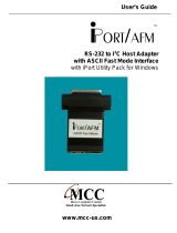
1.1.1 Block Diagram
The C5515 DSP block diagram is shown in Figure 1-1 .
Figure 1-1. Functional Block Diagram
13
SPRUFX5A–October 2010–Revised November 2010 System Control
Submit Documentation Feedback
Copyright © 2010, Texas Instruments Incorporated

Introduction
www.ti.com
1.1.2 CPU Core
The C55x CPU is responsible for performing the digital signal processing tasks required by the
application. In addition, the CPU acts as the overall system controller, responsible for handling many
system functions such as system-level initialization, configuration, user interface, user command
execution, connectivity functions, and overall system control.
Tightly coupled to the CPU are the following components:
• DSP internal memories
– Dual-access RAM (DARAM)
– Single-access RAM (SARAM)
– Read-only memory (ROM)
• FFT hardware accelerator
• Ports and buses
The CPU also manages/controls all peripherals on the device. Refer to the device-specific data manual for
the full list of peripherals.
Figure 1-1 shows the functional block diagram of the DSP and how it connects to the rest of the device.
The DSP architecture uses the switched central resource (SCR) to transfer data within the system.
1.1.3 FFT Hardware Accelerator
The C55x CPU includes a tightly-coupled FFT hardware accelerator that communicates with the C55x
CPU through the use coprocessor instructions. For ease of use, the ROM has a set of C-callable routines
that use these coprocessor instructions to perform 8, 16, 32, 64, 128, or 256-point FFTs. The main
features of the FFT hardware accelerator are:
• Support for 8 to 1024-point (in powers of 2) real and complex-valued FFTs and IFFTs.
• An internal twiddle factor generator for optimal use of memory bandwidth and more efficient
programming.
• Basic and software-driven auto-scaling feature provides good precision vs cycle count trade-off.
• Single-stage and double-stage modes enabling computation of one or two stages in one pass, thus
handling odd power of two FFT widths.
1.1.3.1 Using FFT Accelerator ROM routines
The C5505 includes C-callable routines in ROM to execute FFT and IFFT using the tightly coupled FFT
accelerator. The routines reside in the following address:
Table 1-1.
Address Name Description Calling Convention
0x00ff6cd6 hwafft br Vector bit-reversal void hwafft_br( Int32 *data, Int32 *data_br, Uint16
data_len );
0x00ff6cea hwafft 8pts 8-pt FFT/IFFT Uint16 hwafft_8pts( Int32 *data,Int32 *scratch, Uint16
fft_flag, Uint16 scale_flag);
0x00ff6dd9 hwafft 16pts 16-pt FFT/IFFT Uint16 hwafft_16pts( Int32 *data,Int32 *scratch, Uint16
fft_flag, Uint16 scale_flag);
0x00ff6f2f hwafft 32pts 32-pt FFT/IFFT Uint16 hwafft_32pts( Int32 *data,Int32 *scratch, Uint16
fft_flag, Uint16 scale_flag);
0x00ff7238 hwafft 64pts 64-pt FFT/iFFT Uint16 hwafft_64pts( Int32 *data,Int32 *scratch, Uint16
fft_flag, Uint16 scale_flag);
0x00ff73cd hwafft 128pts 128-pt FFT/IFFT Uint16 hwafft_128pts( Int32 *data,Int32 *scratch,
Uint16 fft_flag, Uint16 scale_flag);
0x00ff75de hwafft 256pts 256-pt FFT/IFFT Uint16 hwafft_256pts( Int32 *data,Int32 *scratch,
Uint16 fft_flag, Uint16 scale_flag);
0x00ff77dc hwafft 512pts 512-pt FFT/iFFT Uint16 hwafft_512pts( Int32 *data,Int32 *scratch,
Uint16 fft_flag, Uint16 scale_flag);
0x00ff7a56 hwafft 1024pts 1024-pt FFT/IFFT Uint16 hwafft_1024pts( Int32 *data,Int32 *scratch,
Uint16 fft_flag, Uint16 scale_flag);
14
System Control SPRUFX5A–October 2010–Revised November 2010
Submit Documentation Feedback
Copyright © 2010, Texas Instruments Incorporated

www.ti.com
Introduction
Note that for the FFT routines, output data is dependent on the return value (T0). If return = 0 output data
is in-place, meaning the result will overwrite the input buffer. If return =1, output data is placed in the
scratch buffer. The 32-bit input and output data consist of 16-bit real and 16-bit imaginary data. If only real
data is used, the imaginary part can be zeroed. The Scale flag determines if the butterfly output is divided
by 2 to prevent overflow at the expense of resolution. For further information on how to use these routines,
see FFT Implementation on the TMS320VC5505, TMS320C5505, and TMS320C5515 DSPs (SPRABB6).
1.1.4 Power Management
Integrated into the C5515/14 DSP are the following power management features:
• One low dropout LDO for analog portions of the device, DSP PLL (V
DDA_PLL
), SAR, and power
management circuits (V
DDA_ANA
): ANA_LDO
• One LDO for DSP core (CV
DD
): DSP_LDO
• One LDO for USB core and PHY (USB_V
DDA1P3
): USB_LDO
• Idle controller with several clock domains:
– CPU domain
– Clock generator domain
– Peripheral domain
– USB domain
– Real-time clock (RTC) domain
• Independent voltage and power domains
• LDOI (LDOs and Bandgap Power Supply)
• Analog POR, SAR, and PLL (V
DDA_ANA
and V
DDA_PLL
)
• Real-time clock core (CV
DDRTC
)
• Digital core (CV
DD
)
• USB core (USB_ V
DD1P3
and USB_V
DDA1P3
)
• USB PHY and USB PLL (USB_V
DDOSC
, USB_V
DDA3P3
, and USB_V
DDPLL
)
• EMIF I/O (DV
DDEMIF
)
• RTC I/O (DV
DDRTC
)
• Rest of the I/O (DV
DDIO
)
1.1.5 Peripherals
The DSP includes the following peripherals:
• Four direct memory access (DMA) controllers, each with four independent channels.
• One external memory interface (EMIF) with 21-bit address and 16-bit data. The EMIF has support for
mobile SDRAM and non-mobile SDRAM single-level cell (SCL) NAND with 1-bit ECC, and multi-level
cell (MLC) NAND with 4-bit ECC.
NOTE: The C5515 can support non-mobile SDRAM under certain circumstances. The C5515
always uses mobile SDRAM initialization but it is able to support SDRAM memories that
ignore the BA0 and BA1 pins for the 'load mode register' command. During the mobile
SDRAM initialization, the device issues the 'load mode register' initialization command to two
different addresses that differ in only the BA0 and BA1 address bits. These registers are the
Extended Mode register and the Mode register. The Extended mode register exists only in
mSDRAM and not in non-mSDRAM. If a non-mobile SDRAM memory ignores bits BA0 and
BA1, the second loaded register value overwrites the first, leaving the desired value in the
Mode register and the non-mobile SDRAM will work with C5515.
• Two serial busses each configurable to support one Multimedia Card (MMC) / Secure Digital
(SD/SDIO) controller, one inter-IC sound bus (I2S) interface with GPIO, or a full GPIO interface.
• One parallel bus configurable to support a 16-bit LCD bridge or a combination of an 8-bit LCD bridge,
a serial peripheral interface (SPI), an I2S, a universal asynchronous receiver/transmitter (UART), and
GPIO.
• One inter-integrated circuit (I2C) multi-master and slave interface with 7-bit and 10-bit addressing
15
SPRUFX5A–October 2010–Revised November 2010 System Control
Submit Documentation Feedback
Copyright © 2010, Texas Instruments Incorporated

System Memory
www.ti.com
modes.
• Three 32-bit timers with 16-bit prescaler; one timer supports watchdog functionality.
• A USB 2.0 slave.
• A 10-bit successive approximation (SAR) analog-to-digital converter with touchscreen conversion
capability.
• One real-time clock (RTC) with associated low power mode.
1.2 System Memory
The DSP supports a unified memory map (program code sections and data sections can be mixed and
interleaved within the entire memory space) composed of both on-chip and external memory. The on-chip
memory consists of 320KB of RAM and 128KB of ROM.
The external memory interface (EMIF) port provides the means for the DSP to access external memory
and devices including: mobile and non-mobile single data rate (SDR) SDRAM, (for limitations, see note in
Section 1.1.5), NOR Flash, NAND Flash and SRAM.
Separate from the program and data space, the DSP also includes a 64K-byte I/O space for peripheral
registers.
1.2.1 Program/Data Memory Map
The device provides 16MB of total address space composed of on-chip RAM, on-chip ROM, and external
memory space supporting a variety of memory types. The on-chip, dual-access RAM allows two accesses
to a given block during the same cycle. The device has 8 blocks of 8K-bytes of dual-access RAM. The
on-chip, single-access RAM allows one access to a given block per cycle. The device has 32 blocks of
8K-bytes of single-access RAM. Attempts to perform two accesses in a cycle to single-access memory will
cause one access to stall until the next cycle. An access is defined as either a read or write operation. For
the most efficient use of DSP processing power (MIPS), it is important to pay attention to the memory
blocks that are being simultaneously accessed by the code and data operations.
The external memory space is divided into five spaces. Each space has a chip select decode signal
(called CS) that indicates an access to the selected space. The external memory interface (EMIF)
supports access to asynchronous memories such as SRAM Flash, mobile SDRAM and SDRAM.
The DSP memory is accessible by different master modules within the DSP, including the device CPU, the
four DMA controllers, and the USB. The DSP memory map as seen by these modules is illustrated in
Figure 1-2.
16
System Control SPRUFX5A–October 2010–Revised November 2010
Submit Documentation Feedback
Copyright © 2010, Texas Instruments Incorporated

0001 0000h
64K Minus 192 Bytes
DARAM
(D)
0009 0000h
SARAM
256K Bytes
External-CS2 Space
(C)
0200 0000h
0300 0000h
0400 0000h
0500 0000h
050E 0000h
128K Bytes Asynchronous (if MPNMC=1)
128K Bytes ROM (if MPNMC=0)
External-CS3 Space
(C)
External-CS4 Space
(C)
External-CS5 Space
(C)
BLOCK SIZE
DMA/USB/LCD
BYTE ADDRESS
(A)
ROM
(if MPNMC=0)
External-CS5
f MPNMC=1)
(C)
Space
(i
1M Minus 128K Bytes Asynchronous
1M Bytes Asynchronous
2M Bytes Asynchronous
4M Bytes Asynchronous
MEMORY BLOCKS
0001 00C0h
MMR (Reserved)
(B)
0100 0000h
External-CS0 Space
(C)(E)
8M Minus 320K Bytes SDRAM/mSDRAM
050F FFFFh
000000h
010000h
800000h
C00000h
E00000h
F00000h
FE0000h
CPU BYTE
ADDRESS
(A)
0000C0h
050000h
FFFFFFh
www.ti.com
System Memory
Figure 1-2. DSP Memory Map
A Address shown represents the first byte address in each block.
B The first 192 bytes are reserved for memory-mapped registers (MMRs).
C Out of the four DMA controllers, only DMA controller 3 has access to the external memory space.
D The USB controller does not have access to DARAM.
E The CS0 space can be accessed by CS0 only or by CS0 and CS1.
1.2.1.1 On-Chip Dual-Access RAM (DARAM)
The DARAM is located in the CPU byte address range 00 00C0h - 00 FFFFh and is composed of eight
blocks of 4K words each (see Table 1-2). Each DARAM block can perform two accesses per cycle (two
reads, two writes, or a read and a write). DARAM can be accessed by the internal program, data, and
DMA buses.
As shown in Table 1-2, the DMA controllers access DARAM at an address offset 0x0001_0000 from the
CPU memory byte address space.
Table 1-2. DARAM Blocks
Memory Block CPU Byte Address Range DMA/USB Controller Byte Address Range
DARAM 0
(1)
00 00C0h - 00 1FFFh 0001 00C0h - 0001 1FFFh
DARAM 1 00 2000h - 00 3FFFh 0001 2000h - 0001 3FFFh
DARAM 2 00 4000h - 00 5FFFh 0001 4000h - 0001 5FFFh
DARAM 3 00 6000h - 00 7FFFh 0001 6000h - 0001 7FFFh
DARAM 4 00 8000h - 00 9FFFh 0001 8000h - 0001 9FFFh
DARAM 5 00 A000h - 00 BFFFh 0001 A000h - 0001 BFFFh
(1)
First 192 bytes are reserved for memory-mapped registers (MMRs).
17
SPRUFX5A–October 2010–Revised November 2010 System Control
Submit Documentation Feedback
Copyright © 2010, Texas Instruments Incorporated

System Memory
www.ti.com
Table 1-2. DARAM Blocks (continued)
Memory Block CPU Byte Address Range DMA/USB Controller Byte Address Range
DARAM 6 00 C000h - 00 DFFFh 0001 C000h - 0001 DFFFh
DARAM 7 00 E000h - 00 FFFFh 0001 E000h - 0001 FFFFh
1.2.1.2 On-Chip Single-Access RAM (SARAM)
The SARAM is located at the CPU byte address range 01 0000h - 04FFFFh and is composed of 32 blocks
of 4K words each (see Table 1-3). Each SARAM block can perform one access per cycle (one read or one
write). SARAM can be accessed by the internal program, data, and DMA buses.
As shown in Table 1-3, the DMA controllers access SARAM at an address offset 0x0008_0000 from the
CPU memory byte address space.
Table 1-3. SARAM Blocks
DMA/USB Controller Byte Address
Memory Block CPU Byte Address Range Range
SARAM 0 01 0000h - 01 1FFFh 0009 0000h - 0009 1FFFh
SARAM 1 01 2000h - 01 3FFFh 0009 2000h - 0009 3FFFh
SARAM 2 01 4000h - 01 5FFFh 0009 4000h - 0009 5FFFh
SARAM 3 01 6000h - 01 7FFFh 0009 6000h - 0009 7FFFh
SARAM 4 01 8000h - 01 9FFFh 0009 8000h - 0009 9FFFh
SARAM 5 01 A000h - 01 BFFFh 0009 A000h - 0009 BFFFh
SARAM 6 01 C000h - 01 DFFFh 0009 C000h - 0009 DFFFh
SARAM 7 01 E000h - 01 FFFFh 0009 E000h - 0009 FFFFh
SARAM 8 02 0000h - 02 1FFFh 000A 0000h - 000A 1FFFh
SARAM 9 02 2000h - 02 3FFFh 000A 2000h - 000A 3FFFh
SARAM 10 02 4000h - 02 5FFFh 000A 4000h - 000A 5FFFh
SARAM 11 02 6000h - 02 7FFFh 000A 6000h - 000A 7FFFh
SARAM 12 02 8000h - 02 9FFFh 000A 8000h - 000A 9FFFh
SARAM 13 02 A000h - 02 BFFFh 000A A000h - 000A BFFFh
SARAM 14 02 C000h - 02 DFFFh 000A C000h - 000A DFFFh
SARAM 15 02 E000h - 02 FFFFh 000A E000h - 000A FFFFh
SARAM 16 03 0000h - 03 1FFFh 000B 0000h - 000B 1FFFh
SARAM 17 03 2000h - 03 3FFFh 000B 2000h - 000B 3FFFh
SARAM 18 03 4000h - 03 5FFFh 000B 4000h - 000B 5FFFh
SARAM 19 03 6000h - 03 7FFFh 000B 6000h - 000B 7FFFh
SARAM 20 03 8000h - 03 9FFFh 000B 8000h - 000B 9FFFh
SARAM 21 03 A000h - 03 BFFFh 000B A000h - 000B BFFFh
SARAM 22 03 C000h - 03 DFFFh 000B C000h - 000B DFFFh
SARAM 23 03 E000h - 03 FFFFh 000B E000h - 000B FFFFh
SARAM 24 04 0000h - 04 1FFFh 000C 0000h - 000C 1FFFh
SARAM 25 04 2000h - 04 3FFFh 000C 2000h - 000C 3FFFh
SARAM 26 04 4000h - 04 5FFFh 000C 4000h - 000C 5FFFh
SARAM 27 04 6000h - 04 7FFFh 000C 6000h - 000C 7FFFh
SARAM 28 04 8000h - 04 9FFFh 000C 8000h - 000C 9FFFh
SARAM 29 04 A000h - 04 BFFFh 000C A000h - 000C BFFFh
SARAM 30 04 C000h - 04 DFFFh 000C C000h - 000C DFFFh
SARAM 31 04 E000h - 04 FFFFh 000C E000h - 000C FFFFh
18
System Control SPRUFX5A–October 2010–Revised November 2010
Submit Documentation Feedback
Copyright © 2010, Texas Instruments Incorporated

www.ti.com
System Memory
1.2.1.3 On-Chip Single-Access Read-Only Memory (SAROM)
The zero-wait-state ROM is located at the CPU byte address range FE 0000h - FF FFFFh. The ROM is
composed of four 16K-word blocks, for a total of 128K-bytes of ROM. Each ROM block can perform one
access per cycle (one read or one write). ROM can be accessed by the internal program or data buses,
but not the DMA buses. The ROM address space can be mapped by software to the external memory or
to the internal ROM via the MPNMC bit in the ST3 status register.
The standard device includes a Bootloader program resident in the ROM and the bootloader code is
executed immediately after hardware reset. When the MPNMC bit field of the ST3 status register is set
through software, the on-chip ROM is disabled and not present in the memory map, and byte address
range FE 0000h - FF FFFFh is directed to external memory space (extends CS5 address reach). A
hardware reset always clears the MPNMC bit, so it is not possible to disable the ROM at hardware reset.
However, the software reset instruction does not affect the MPNMC bit. The ROM can be accessed by the
program and data buses. Each SAROM block can perform one word read access per cycle.
Table 1-4. SAROM Blocks
Memory Block CPU Byte Address Range CPU Word Address Range
SAROM0 FE 0000h - FE 7FFFh 7F 0000h - 7F 3FFFh
SAROM1 FE 8000h - FE FFFFh 7F 4000h - 7F 7FFFh
SAROM2 FF 0000h - FF 7FFFh 7F 8000h - 7F BFFFh
SAROM3 FF 8000h - FF FFFFh 7F C000h - 7F FFFFh
1.2.1.4 External Memory
The external memory space of the device is located at the byte address range 05 0000h - FF FFFFh. The
external memory space is divided into five chip select spaces. The synchronous space is activated by one
chip select pin (EM_CS0) or by a pair of chip selects pins (EM_CS0 and EM_CS1). Each asynchronous
chip select space has a corresponding chip select pin (called EMIF_CS[2:5]) that is activated during an
access to the chip select space.
The external memory interface (EMIF) provides the means for the DSP to access external memories and
other devices including: NOR Flash, NAND Flash, SRAM, mSDRAM, and SDRAM (see section 1.5 for
limitations). Before accessing external memory, you must configure the EMIF through its registers. For
more detail on the EMIF, see the TMS320C5515/14/05/04 DSP External Memory Interface (EMIF) User’s
Guide (SPRUGU6).
As described in Section 1.2.1.3, when the MPNMC bit field of the ST3 status register is cleared (default),
the byte address range FE 0000h - FF FFFFh is reserved for the on-chip ROM, which decreases the
addressable size for EM_CS5.
The EMIF provides a configurable 16-bit (synchronous or asynchronous) or 8-bit (asynchronous only) data
bus, an address bus width of up to 21-bits, and five dedicated chip selects, along with memory control
signals. To maximize power savings, the I/O pins of the EMIF can be operated at lower voltage
independently of other I/O pins on the DSP. Further power savings may be achieved by setting the EMIF
I/O pins to have slow slew rate, as described in Section 1.7.3.4.
1.2.1.4.1 Asynchronous EMIF Interface
The EMIF provides a configurable 16- or 8-bit data bus with address bus width of up to 21-bits, and six
dedicated chip selects, along with memory control signals. The cycle timings of the asynchronous
interface are fully programmable, allowing for access to a wide range of devices including NAND flash,
NOR flash, and SRAM as well as other asynchronous devices such as a TI DSP HPI interface. In NAND
mode, the asynchronous interface supports 1-bit ECC for 8- and 16-bit NAND flash and 4-bit ECC for 8-bit
NAND flash.
1.2.1.5 Synchronous EMIF Interface
The EMIF provides a 16-bit data bus with one or two dedicated chip selects for mSDRAM. Non-mobile
SDRAM can be supported under certain circumstances. The C5515 always uses a mobile SDRAM
initialization command sequence, but it is able to support SDRAM memories that ignore the BA0 and BA1
19
SPRUFX5A–October 2010–Revised November 2010 System Control
Submit Documentation Feedback
Copyright © 2010, Texas Instruments Incorporated

Device Clocking
www.ti.com
pins for the load mode register command. During the mobile SDRAM initialization, the device issues the
load mode register initialization command to two different addresses that differ in only the BA0 and BA1
address bits. These registers are the Extended Mode register and the Mode register. The extended mode
register exists only in mSDRAM, and not in non-mSDRAM. If a non-mobile SDRAM memory ignores bits
BA0 and BA1, the second loaded register value overwrites the first, leaving the desired value in the mode
register and the non-mobile SDRAM works with the device.
Some timing parameters are programmable such as the refresh rate and CAS latencies. The EMIF
supports up to 100 MHz SDCLK and has the ability to run the SDCLK at half the system clock to meet the
EMIF I/O timing requirements and/or at lower power if a slower SDCLK can be used. Detailed information
is available in the Clock Control section of the TMS320C5515/14/05/04 DSP External Memory Interface
(EMIF) User's Guide (SPRUGU6).
1.2.2 I/O Memory Map
The C5x DSP has a separate memory map for peripheral and system registers, called I/O space. This
space is 64K-words in length and is accessed via word read and write instructions dedicated for I/O
space.
Separate documentation for I/O space registers related to each peripheral exists and is listed in the
preface of this guide. System registers, which provide system-level control and status, are described in
detail in other sections throughout this guide. Unused addresses in I/O space should be treated as
reserved and should not be accessed. Accessing unused I/O space addresses may stall or hang the DSP.
Each of the four DMA controllers has access to a different set of peripherals and their I/O space registers.
This is shown in Section 1.7.4.
NOTE: Writting to I/O space registers incurs in at least 2 CPU cycle latency. Thus, when
configuring peripheral devices, wait at least two cycles before accessing data from the
peripheral. When more than one peripheral register is updated in a sequence, the CPU only
needs to wait following the final register write. For example, if the EMIF is being
reconfigured, the CPU must wait until the very last EMIF register update takes effect before
trying to access the external memory. The users should consult the respective peripheral
user's guide to determine if a peripheral requires additional initialization time.
Before accessing any peripheral register, make sure the peripheral is not held in reset and its internal
clock is enabled. The peripheral reset control register (Section 1.7.5.2) and the peripheral clock gating
control registers (Section 1.5.3.2.1) control these functions. Accessing a peripheral whose clocks are
gated will either return the value of the last address read from the peripheral (when the clocks were last
ON) or it may possibly hang the DSP -- depending on the peripheral.
1.3 Device Clocking
1.3.1 Overview
The DSP requires two primary reference clocks: a system reference clock and a USB reference clock. The
system clock, which is used by the CPU and most of the DSP peripherals, is controlled by the system
clock generator. The system clock generator features a software-programmable PLL multiplier and several
dividers. The system clock generator accepts an input reference clock from the CLKIN pin or the output
clock of the 32.768-KHz real-time clock (RTC) oscillator. The selection of the input reference clock is
based on the state of the CLK_SEL pin. The CLK_SEL pin is required to be statically tied high or low and
cannot change dynamically after reset. The system clock generator can be used to modify the system
reference clock signal according to software-programmable multiplier and dividers. The resulting clock
output, the DSP system clock, is passed to the CPU, peripherals, and other modules inside the DSP.
Alternatively, the system clock generator can be fully bypassed and the input reference clock can be
passed directly to the DSP system clock. The USB reference clock is generated using a dedicated on-chip
oscillator with a 12 MHz external crystal connected to the USB_MXI and USB_MXO pins. This crystal is
not required if the USB peripheral is not being used. The USB oscillator cannot be used to provide the
system reference clock.
The RTC oscillator generates a clock when a 32.768-KHz crystal is connected to the RTC_XI and
20
System Control SPRUFX5A–October 2010–Revised November 2010
Submit Documentation Feedback
Copyright © 2010, Texas Instruments Incorporated
/