11
Operation continued
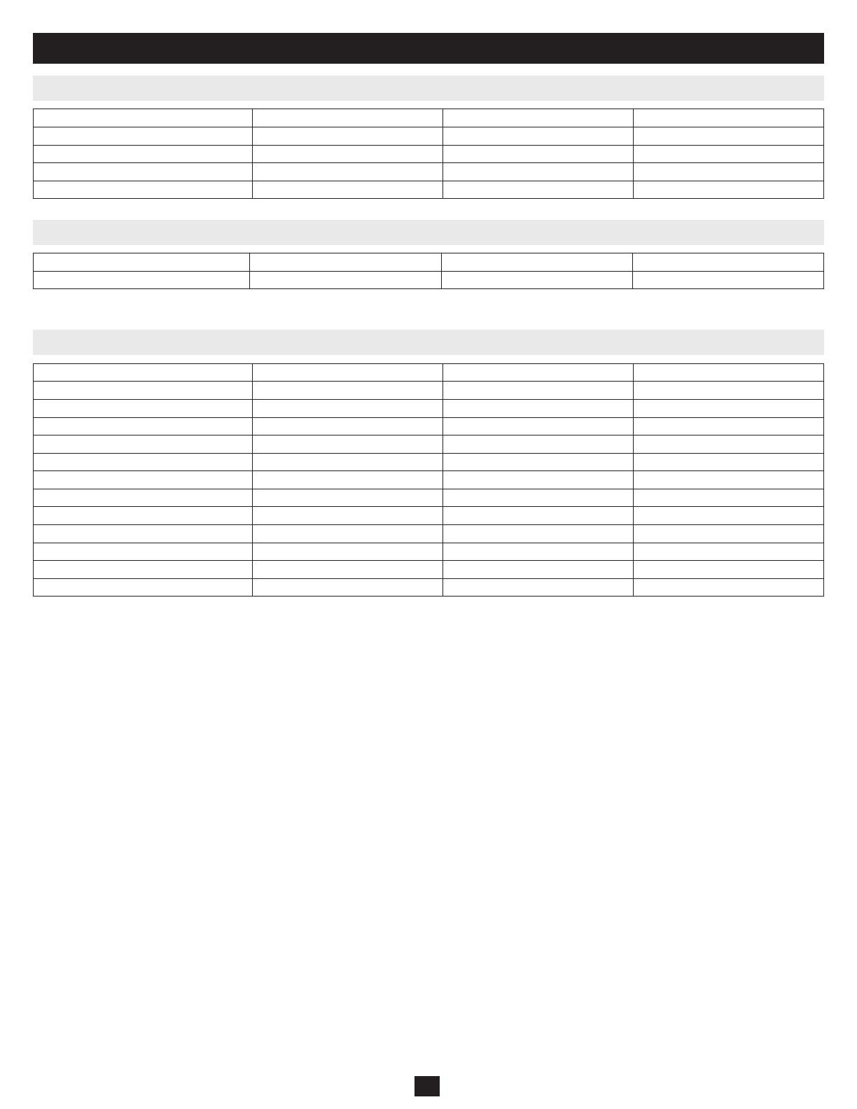
Select Voltage
SRAM Exist
TempStatus
Description Address Value Unit
Selected Output Voltage 0x0471 0-999 Voltage
Select Output Voltage 1 0x0472 0-999 Voltage
Select Output Voltage 2 0x0473 0-999 Voltage
Select Output Voltage 3 0x0474 0-999 Voltage
Description Address Value Unit
SRAM EXIST 0x0475 0: Doesn’t Exist 1: Exists
Note: Currently, this field is not supported by UPS.
Description Address Value Unit
TempStatus Byte 1, 2 0x0476 Low: Byte 1, Hi: Byte 2
TempStatus Byte 3, 4 0x0477 Low: Byte 3, Hi: Byte 4
TempStatus Byte 5, 6 0x0478 Low: Byte 5, Hi: Byte 6
TempStatus Byte 7, 8 0x0479 Low: Byte 7, Hi: Byte 8
TempStatus Byte 9, 10
0x047A
Low: Byte 9, Hi: Byte 10
TempStatus Byte 11, 12 0x047B Low: Byte 12, Hi: Byte 12
TempStatus Byte 13, 14 0x047C Low: Byte 13, Hi: Byte 14
TempStatus Byte 15, 16 0x047D Low: Byte 15, Hi: Byte 16
TempStatus Byte 17, 18 0x047E Low: Byte 17, Hi: Byte18
TempStatus Byte 19, 20 0x047F Low: Byte 19, Hi: Byte 20
Reserved 0x0480
Reserved 0x0481
Temp Byte 1 (Lo): R Phase Inverter Temperature
Temp Byte 2 (Hi): B0: Temperature Warning (>=75C)
B1: High Temperature Shutdown (>=85C)
B2: Inverter Voltage Too Low
B3: Inverter Voltage Too High
B4: Overload Warning
B5: Overload Shutdown
B6: Inverter Fuse Fail Shutdown
B7: Inverter PCB Communication Abnormal
Temp Byte 3 (Lo): S Phase Inverter Temperature
Temp Byte 4 (Hi): B0: Temperature Warning (>=75C)
B1: High Temperature Shutdown (>=85C)
B2: Inverter Voltage Too Low
B3: Inverter Voltage Too High
B4: Overload Warning
B5: Overload Shutdown
B6: Inverter Fail Shutdown
B7: Parallel Communication Abnormal
Temp Byte 5 (Lo): T Phase Inverter Temperature
Temp Byte 6 (Hi): B0: Temperature Warning (>=75C)
B1: High Temperature Shutdown (>=85C)
B2: Inverter Voltage Too Low
B3: Inverter Voltage Too High
B4: Overload Warning
B5: Overload Shutdown
B6: Inverter Freq Abnormal Shutdown
B7: Parallel Communication Fail
Temp Byte 7 (Lo): B3..B0: The Summary of UPS Run at Inverter Test Mode
B7..B4: The Summary of UPS at Inverter Mode
Temp Byte 8 (Hi): B0: Power Fail
B1: EPO Happened
B2: MB_ON (To Bypass)
B3: Low Battery Warning
B4: Battery Low Shutdown
B5: Master UPS (Output Synch)
B6: Inverter DC Bus Abnormal Shutdown
B7: Short Circuit Shutdown
Temp Byte 9 (Lo): Heatsink Temperature
Temp Byte 10 (Hi): B0: Bypass Voltage Over
B1: Bypass Voltage Under
B2: Bypass Freq Abnormal
B3: Bypass Phase Abnormal
B4: Rectier Voltage Over
B5: Rectier Voltage Under
B6: Rectier Freq Abnormal
B7: Rectier Phase Abnormal
Temp Byte 11 (Lo): Ambient Temperature
Temp Byte 12 (Hi): B0: Bypass Voltage Over
B1: Bypass Voltage Under
B2: SSW at Bypass Side
B3: SSW at Inverter Side
B4: Rectier Voltage Over
B5: Rectier Voltage Under
B6: Rectier Input Over Current
B7: Rectier Input Current Unbalanced


