Elixir M2Y2G64CB8HC5N-CG Datasheet
- Category
- Memory modules
- Type
- Datasheet
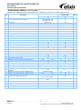
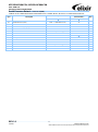
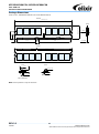
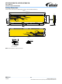
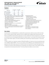
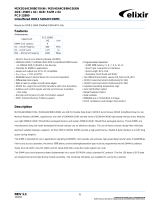
The Elixir M2Y2G64CB8HC5N-CG is a high-performance DDR3 SDRAM module designed for use in applications operating up to 667MHz clock speeds, achieving data transfer rates of up to 1333 Mbps. With its 2GB capacity and 256Mx64 organization, it offers ample memory for demanding tasks and supports various operation modes, including Burst Read and Write. The module features programmable CAS latency, burst type, and burst length, allowing for flexible configuration to optimize performance.
The Elixir M2Y2G64CB8HC5N-CG is a high-performance DDR3 SDRAM module designed for use in applications operating up to 667MHz clock speeds, achieving data transfer rates of up to 1333 Mbps. With its 2GB capacity and 256Mx64 organization, it offers ample memory for demanding tasks and supports various operation modes, including Burst Read and Write. The module features programmable CAS latency, burst type, and burst length, allowing for flexible configuration to optimize performance.


-
 1
1
-
 2
2
-
 3
3
-
 4
4
-
 5
5
-
 6
6
-
 7
7
-
 8
8
-
 9
9
-
 10
10
-
 11
11
-
 12
12
-
 13
13
-
 14
14
-
 15
15
-
 16
16
-
 17
17


Elixir M2Y2G64CB8HC5N-CG Datasheet
- Category
- Memory modules
- Type
- Datasheet
The Elixir M2Y2G64CB8HC5N-CG is a high-performance DDR3 SDRAM module designed for use in applications operating up to 667MHz clock speeds, achieving data transfer rates of up to 1333 Mbps. With its 2GB capacity and 256Mx64 organization, it offers ample memory for demanding tasks and supports various operation modes, including Burst Read and Write. The module features programmable CAS latency, burst type, and burst length, allowing for flexible configuration to optimize performance.
Ask a question and I''ll find the answer in the document
Finding information in a document is now easier with AI
Related papers
-
 Elixir M2F2G64CB88DHN-CG Datasheet
-
 Elixir M2F4G64CB8HG5N-CG Datasheet
-
 Elixir M2X4G64CB8HG9N-DG User manual
-
 Elixir M2F2G64CB8HA4N-CG Datasheet
-
 Elixir M2Y2G64CB8HA9NDG User manual
-
 Elixir M2N2G64CB8HA5N-CG Datasheet
-
 Elixir M2S4G64CB8HG5N-CG Datasheet
-
Elixir M2S8G64CB8HB5N-CG Datasheet
-
 Elixir M2X4G64CB8HG5N-DG User manual
-
 Elixir M2F2G64CB88B7N-CG Datasheet


Other documents
-
Transcend TS1GLK72V6H Datasheet
-
-
 Hynix HMT41GU7MFR8C-H9 Datasheet
-
 Hynix HMT351U6CFR8C-H9N0 User manual
-
-
 Hynix HMT351U7CFR8A-PBT0 Datasheet
-
 Hynix HMT451U7AFR8C-PBT0 Datasheet
-
Super Talent Technology W1333UA2GV Datasheet
-
Samsung M471B1G73AH0 User manual
-


