
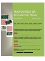
PEX/PIO/PISO-DA
Series Card User Manual
Analog Output Boards Version 3.1, Oct. 2013
SUPPORTS
Board includes PIO-DA4, PIO-DA8, PIO-DA16, PIO-DA4U, PIO-DA8U,
PIO-DA16U, PISO-DA4U, PISO-DA8U, PISO-DA16U, PEX-DA4, PEX-DA8 and
PEX-DA16.
WARRANTY
All products manufactured by ICP DAS are warranted against defective materials
for a period of one year from the date of delivery to the original purchaser.
WARNING
ICP DAS assumes no liability for damages consequent to the use of this product.
ICP DAS reserves the right to change this manual at any time without notice.
The information furnished by ICP DAS is believed to be accurate and reliable.
However, no responsibility is assumed by ICP DAS for its use, nor for any
infringements of patents or other rights of third parties resulting from its use.
COPYRIGHT
Copyright © 2013 by ICP DAS. All rights are reserved.
TRADEMARK
Names are used for identification only and may be registered trademarks of their
respective companies.
CONTACT US
If you have any question, please feel to contact us. We will give you quick
response within 2 workdays.
Email: service@icpdas.com, service.icpdas@gmail.com

PEX/PIO/PISO-DA Series Card
Analog Output Boards
User Manual/ Ver. 3.1/ Oct. 2013/ PMH-0010-31/ Page: 2
TABLE OF CONTENTS
PACKING LIST ......................................................................................................................................................... 5
RELATED INFORMATION ...................................................................................................................................... 5
1. INTRODUCTION ........................................................................................................................................... 6
1.1 FEATURES .......................................................................................................................................................... 7
1.2 COMPARISON TABLE ........................................................................................................................................... 8
1.3 SPECIFICATIONS ................................................................................................................................................. 9
2. HARDWARE CONFIGURATION ................................................................................................................ 11
2.1 BOARD LAYOUT ................................................................................................................................................ 11
2.2 COUNTER ARCHITECTURE ................................................................................................................................. 13
2.3 INTERRUPT OPERATION .................................................................................................................................... 14
2.3.1 Interrupt Block Diagram
.......................................................................................................................... 15
2.3.2 INT_CHAN_0/1
......................................................................................................................................... 16
2.3.3 Initial_High, Ative_Low Interrupt Source
............................................................................................. 17
2.3.4 Initial_Low, Ative_High Interrupt Source
............................................................................................. 18
2.3.5 Multiple Interrupt Source
........................................................................................................................ 19
2.4 D/I/O BLOCK DIAGRAM .................................................................................................................................... 21
2.4.1
D/I Port Architecture (CON2)
.................................................................................................................. 22
2.4.2
D/O Port Architecture (CON1)
................................................................................................................. 23
2.5 D/A ARCHITECTURE ......................................................................................................................................... 24
2.6 D/A CONVERSION OPERATIONS ........................................................................................................................ 25
2.6.1
Output Range and Resolution
................................................................................................................. 27
2.6.2
± 10 V Voltage Output
.............................................................................................................................. 28
2.6.3
± 5 V Voltage Output
................................................................................................................................ 28
2.6.4
0~10 V Voltage Output
............................................................................................................................ 28
2.6.5
0~5 V Voltage Output
.............................................................................................................................. 28
2.6.6
0~20 mA Current Output
........................................................................................................................ 29
2.6.7
4~20 mA Current Output
........................................................................................................................ 29
2.6.8
No VR and No Jumper Design
................................................................................................................ 29
2.6.9
Factory Software Calibration
................................................................................................................... 31
2.6.10
User Software Calibration
................................................................................................................... 33
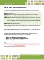
2.6.11
Voltage Output Connection
................................................................................................................. 34

PEX/PIO/PISO-DA Series Card
Analog Output Boards
User Manual/ Ver. 3.1/ Oct. 2013/ PMH-0010-31/ Page: 3
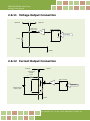
2.6.12
Current Output Connection
................................................................................................................ 34
2.7 CARD ID SWITCH .............................................................................................................................................. 35
2.8 PIN ASSIGNMENTS ............................................................................................................................................ 36
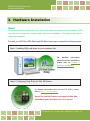
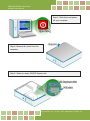
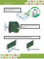
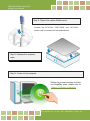
3. HARDWARE INSTALLATION .................................................................................................................... 37
4. SOFTWARE INSTALLATION ...................................................................................................................... 41
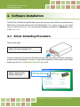
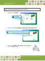
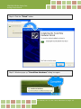
4.1 DRIVER INSTALLING PROCEDURE ...................................................................................................................... 41
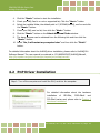
4.2 PNP DRIVER INSTALLATION .............................................................................................................................. 43
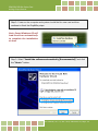
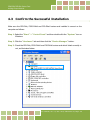
4.3 CONFIRM THE SUCCESSFUL INSTALLATION ......................................................................................................... 46
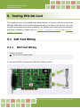
5. TESTING PIO-DA CARD ............................................................................................................................. 47
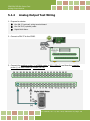
5.1 SELF-TEST WIRING .......................................................................................................................................... 47
5.1.1 DIO Test Wiring
........................................................................................................................................ 47
5.1.2 Analog Output Test Wiring
...................................................................................................................... 48
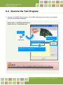
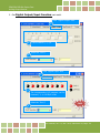
5.2 EXECUTE THE TEST PROGRAM ........................................................................................................................... 49
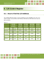
6. I/O CONTROL REGISTER .......................................................................................................................... 52
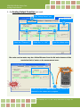
6.1 HOW TO FIND THE I/O ADDRESS ...................................................................................................................... 52
6.1.1 PIO_PISO.EXE Utility for Windows
........................................................................................................ 53
6.1.2 PIO_DriverInit
........................................................................................................................................... 54
6.1.3 PIO_GetConfigAdressSpace
.................................................................................................................... 56
6.1.4 Show_PIO_PISO
....................................................................................................................................... 57
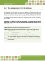
6.2 THE ASSIGNMENT OF I/O ADDRESS .................................................................................................................. 58
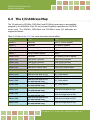
6.3 THE I/O ADDRESS MAP .................................................................................................................................... 60
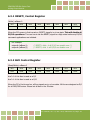
6.3.1
RESET\ Control Register
.......................................................................................................................... 61
6.3.2 AUX Control Register
.................................................................................................................................... 61
6.3.3 Aux Data Register
......................................................................................................................................... 62
6.3.4 INT Mask Control Register
........................................................................................................................... 62
6.3.5 Aux Status Register
...................................................................................................................................... 63
6.3.6 Interrupt Polarity Register
........................................................................................................................... 63
6.3.7 Read/Write 8254 Register
............................................................................................................................ 64
6.3.8 Read Card ID Register
.................................................................................................................................. 65
6.3.9 Digital Input Register
................................................................................................................................... 66
6.3.10 Digital Output Register
.............................................................................................................................. 66
6.3.11 D/A Select Register
..................................................................................................................................... 67
6.3.12 D/A Data Output Register
......................................................................................................................... 68
7. DEMO PROGRAM ......................................................................................................................................... 69
7.1 DEMO PROGRAM FOR WINDOWS ....................................................................................................................... 69

PEX/PIO/PISO-DA Series Card
Analog Output Boards
User Manual/ Ver. 3.1/ Oct. 2013/ PMH-0010-31/ Page: 4
7.2 DEMO PROGRAM FOR DOS ............................................................................................................................... 71
APPENDIX: DAUGHTER BOARD ......................................................................................................................... 73
A1. DB-37 and DN-37
............................................................................................................................................. 73
A2. DB-8125
............................................................................................................................................................ 73
A3. DB-16P Isolated Input Board
......................................................................................................................... 74
A5. DB-16R Relay Board
........................................................................................................................................ 75
A6. DB-24PR/DB-24POR/DB-24C Power Relay Board
........................................................................................ 76

PEX/PIO/PISO-DA Series Card
Analog Output Boards
User Manual/ Ver. 3.1/ Oct. 2013/ PMH-0010-31/ Page: 5
Packing List
The shipping package includes the following items:
One multi-function card as follows:
PEX-DA series:
PEX-DA4/ PEX-DA8/ PEX-DA16
PIO-DAxU series:
PIO-DA4U/ PIO-DA8U/ PIO-DA16U
PISO-DAxU series:
PISO-DA4U/ PISO-DA8U/ PISO-DA16U
One printed Quick Start Guide
One software utility CD
One CA-4002 D-Sub Connect
Related Information
Product Page:
http://www.icpdas.com/root/product/solutions/pc_based_io_board/pci/pio-da4.html
Documentation and Software for PIO-DA series classic:
CD:\NAPDOS\PCI\PIO-DA\
http://ftp.icpdas.com/pub/cd/iocard/pci/napdos/pci/pio-da/
Documentation and Software for UniDAQ SDK:
CD:\NAPDOS\PCI\UniDAQ\
http://ftp.icpdas.com/pub/cd/iocard/pci/napdos/pci/unidaq/
★
Note!!
If any of these items is
missing or damaged, contact
the dealer from whom you
purchased the product. Save
the shipping materials and
carton in case you want to
ship or store the product in
the future.

PEX/PIO/PISO-DA Series Card
Analog Output Boards
User Manual/ Ver. 3.1/ Oct. 2013/ PMH-0010-31/ Page: 6
1. Introduction
The PEX-DA, PISO-DAxU and PIO-DAxU series cards (PCI Express/Universal PCI versions) are
compatible with the PIO-DAx cards (PCI versions) and most users can replace the PIO-DAx by PEX-DA,
PISO-DAxU or PIO-DAxU directly without software/driver modification. Please refer to user manual
(ch 1.1) for the compatibility information.
The PISO-DA series adds high-voltage isolation design that offers a durable ability to keep users'
computers safe from unexpected surge. It is the built-in high-quality isolation components that make
PISO-DA series featuring 2500 V
DC
bus-typed isolation! For the PEX-DA, PIO-DA and the PISO-DA
series, their voltage output range is from -10 V to +10 V, and their current output range is from 0 to
20 mA. In addition, These cards also feature the following advantages by ICP DAS's innovation:
1. Accurate and easy-to-use calibration.
ICP DAS provides the software calibration instead of the manual calibration so that no jumpers
and trim-pots are required anymore. The calibration information can be saved in EEPROM for
long-term use.
2. Individual channel configuration.
In other words, every channel can be individually configured as voltage output or current
output!
3. Card ID.
ICP DAS provides the card ID function for PEX-DA, PISO-DAxU and PIO-DAxU (version 1.1 or
above) series. Users can set card ID for each card and then recognize them one by one when
more than two boards are used in a computer.
Note: This card needs a 12 V power supply, which can be found in either a
regular PC or an Industrial PC.

PEX/PIO/PISO-DA Series Card
Analog Output Boards
User Manual/ Ver. 3.1/ Oct. 2013/ PMH-0010-31/ Page: 7
1.1 Features
Supports +5 V PCI bus for PIO-DA4/DA8/DA16
16/8/4 channels, 14-bit analog output
Voltage output range: ± 10 V
Current output range: 0 ~ 20 mA (sink)
Two pacer timer interrupt source
Double-buffered D/A latch
Software calibration
16-channel DI, 16-channel DO
One D-Sub connector, two 20-pin flat cable connectors
Connects directly to DB-16P, DB-16R, DB-24C, DB-24PR and DB-24POR
[PISO-DA16U/DA8U/DA4U only]
Built-in DC/DC converter with 3000 V
DC
isolation
Supports both +5 V and +3.3 V PCI bus
2500 V
DC
bus-type and power isolation protection
Digital input port can be set to pull-high or pull-low
Card ID function.
[PIO-DA16U/DA8U/DA4U, PEX-DA16/DA8/DA4 only]
Supports both +5 V and +3.3 V PCI bus for PIO-DA16U/DA8U/DA4U
Supports PCI Express x 1 for PEX-DA16/DA8/DA4
Digital input port can be set to pull-high or pull-low
Card ID function

PEX/PIO/PISO-DA Series Card
Analog Output Boards
User Manual/ Ver. 3.1/ Oct. 2013/ PMH-0010-31/ Page: 8
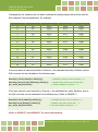
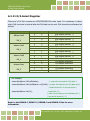
1.2 Comparison Table
Comparison Table of the Different Version Information:
Version
D/I Register
Pin Assignment
Card ID
PIO-DA4
PIO-DA8
PIO-DA16
-
0xE0/E4/E8/EC
0xF0/F4/F8/FC
A. GND
(CN3.5/10/15/24/29)
N/A
PIO-DA4U
PIO-DA8U
PIO-DA16U
V1.0
0xE0/E4/E8/EC
0xF0/F4/F8/FC
A. GND
(CN3.5/10/15/24/29)
N/A
PIO-DA4U
PIO-DA8U
PIO-DA16U
V1.1
0xE0/E4/E8/EC
0xF0/F4/F8/FC
A. GND
(CN3.5/10/15/24/29)
Yes
PIO-DA4U
PIO-DA8U
PIO-DA16U
V1.2 or above
0xE0/E4
A. GND
(CN3.5/10/15)
Yes
PISO-DA4U
PISO-DA8U
PISO-DA16U
V1.3 or above
0xE0/E4
A. GND
(CN3.5/10/15/24/29)
Yes
PEX-DA4
PEX-DA8
PEX-DA16
V1.0
0xE0/E4
A. GND
(CN3.5/10/15)
Yes

PEX/PIO/PISO-DA Series Card
Analog Output Boards
User Manual/ Ver. 3.1/ Oct. 2013/ PMH-0010-31/ Page: 9
1.3 Specifications
Model Name
PEX-DA4/DA8/DA16
PIO-DA4U/DA8U/DA16U
PISO-DA4U/DA8U/DA16U
Analog Output
Isolation
N/A
N/A
2500 V (Bus Type)
Compatibility
4/8/16 independent
Resolution
14-bit
Accuracy
0.04% of FSR ± 2 LSB @ 25 °C, ± 10 V
Output Rang
Voltage: +/- 10 V
Current: 0 ~ 20 mA
Output Driving
± 5 mA
Slew Rate
0.71 V/µs
Output Impedance
0.1 Ω max.
Operating Mode
Software
Digital Input
Channels
16-ch
Compatibility
5 V/TTL
Input Voltage
Logic 0: 0.8 V max.
Logic 1: 2.0 V min.
Response Speed
200 KHz
1.0 MHz (Typical)
Digital Output
Channels
16-ch
Compatibility
5 V/CMOS
5 V/TTL
Output
Voltage
Logic 0
0.1 V max.
0.4 V max.
Logic 1
4.4 V min.
2.4 V min.
Output
Capability
Sink
6 mA @ 0.33 V
2.4 mA @ 0.8 V
Source
6 mA @ 4.77 V
0.8 mA @ 2.0 V
Response Speed
200 KHz
1.0 MHz (Typical)
Timer/Counter
Channels
3
Resolution
16-bit
Compatibility
5 V/TTL
Reference Clock
Internal: 4 MHz

PEX/PIO/PISO-DA Series Card
Analog Output Boards
User Manual/ Ver. 3.1/ Oct. 2013/ PMH-0010-31/ Page: 10
Model Name
PEX-DA4/DA8/DA16
PIO-DA4U/DA8U/DA16U
PISO-DA4U/DA8U/DA16U
General
Bus Type
PCI Express x1
3.3V/5V Universal PCI, 32-bit, 33MHz
Data Bus
8-bit
Card ID
Yes (4-bit)
Yes (4-bit) for Version
1.1 or above
Yes (4-bit)
I/O Connector
Female DB37 x 1,
Male 20-bit ribbon x 2
Dimensions
(L x W )
188 mmx 97 mm
188 mmx 97 mm
(Version 1.1 or above)
180 mmx 97 mm
Power
Consumption
600 mA @ +5 V (PEX-DA4/PIO-DA4U)
800 mA @ +5 V (PEX-DA8/PIO-DA8U)
1400 mA @ +5 V (PEX-DA16/PIO-DA16U)
2200 mA @ +5 V (PISO-DA4U)
2400 mA @ +5 V(PISO-DA8U)
3000 mA @ +5 V(PISO-DA16U)
Operating
Temperature
0 ~ 60 °C
Storage
Temperature
-20 ~ 70 °C
Humidity
5 ~ 85% RH, non-condensing

PEX/PIO/PISO-DA Series Card
Analog Output Boards
User Manual/ Ver. 3.1/ Oct. 2013/ PMH-0010-31/ Page: 11
2. Hardware Configuration
2.1 Board Layout
PIO-DAx Board Layout.
CON1
CON2
CON3
PCI BUS
PIO-DA16
PIO-DA8
PIO-DA4
12
1920
12
1920
DI
DO
Note:
CON1: 16-channel D/O.
CON2: 16-channel D/I.
CON3: 4/8/16-channel D/A converter voltage/current output.

PEX/PIO/PISO-DA Series Card
Analog Output Boards
User Manual/ Ver. 3.1/ Oct. 2013/ PMH-0010-31/ Page: 12
PIO-DAxU and PISO-DAxU Board Layout.
CON1
CON2
CON3
Universal PCI BUS
12
1
9
2
0
12
1
9
2
0
DI
DO
JP1
SW1
ON
1 2 3 4
PEX-DA Board Layout.
CON1
CON2
CON3
PCI Express
12
1
9
2
0
12
1
9
2
0
DI
DO
JP1
SW1
ON
1 2 3 4
Note:
CON1: 16-channel D/O.
CON2: 16-channel D/I.
CON3: 4/8/16-channel D/A converter voltage/current output.
SW1: Card ID.
JP1: Pull-high/pull-low resisters for DI.

PEX/PIO/PISO-DA Series Card
Analog Output Boards
User Manual/ Ver. 3.1/ Oct. 2013/ PMH-0010-31/ Page: 13
2.2 Counter Architecture
There is a single 8254(Timer/Counter) chip on the PEX/PIO/PISO-DA series board and
provides two interrupt sources. The first is a 16-bit timer output (INT0) and the other one is
a 32-bit timer output (INT1). The block diagram is shown below:
OUT0
CLK0
GATE0
Counter0
OUT1
CLK1
GATE1
Counter1
OUT2
CLK2
GATE2
Counter2
Vcc
INT0
INT1
4MHz
8254 Timer/Counter

PEX/PIO/PISO-DA Series Card
Analog Output Boards
User Manual/ Ver. 3.1/ Oct. 2013/ PMH-0010-31/ Page: 14
2.3 Interrupt Operation
There are two interrupt sources included in the PEX-DA and PIO/PISO-DAxU series. These
two signals are named as INT0 and INT1, and their signal sources are as follows:
INT0: 8254 counter0 output (Refer to Sec. 2.2)
INT1: 8254 counter2 output (Refer to Sec. 2.2)
If only one interrupt signal source is used, the interrupt service routine doesn’t have to
identify the interrupt source. Refer to DEMO3.C and DEMO4.C for more information.
If there is more than one interrupt source, the interrupt service routine has to identify the
active signals in the following manner: (Refer to DEMO5.C and DEMO6.C)
1. Read the new status of all interrupt signal sources
2. Compare the new status with the old status to identify the active signals
3. If INT0 is active, service it
4. If INT1 is active, service it
5. Save the new status to replace the old status
Note:
If the interrupt signal is too short, the new status may be the same as the old status. In
that situation, the interrupt service routine will not be able to identify which interrupt
source is active, so the interrupt signal must be hold_active for long enough until the
interrupt service routine is executed. This hold_time is different for different OS versions.
The hold_time can be as short as a micro-second or as long as second. In general, 20 mS
should be long enough for all OS version.

PEX/PIO/PISO-DA Series Card
Analog Output Boards
User Manual/ Ver. 3.1/ Oct. 2013/ PMH-0010-31/ Page: 15
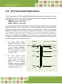
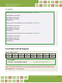
2.3.1 Interrupt Block Diagram
INT\
Level_trigger
INT_CHAN_0
INT_CHAN_1
initial_low
active_high
(to PEX/PCI slot)
The interrupt output signal of PEX-DA and PIO/PISO-DAxU series cards, INT\, is set to
Level-Trigger and Active_Low. If INT\ generates a low_pulse, the PIO-DA4/8/16 will
interrupt the PC once each time. If INT\ is fixed at low_level, the PEX-DA and
PIO/PISO-DAxU series will interrupt the PC continuously. So for the signal pulse_type for
INT_CHAN_0/1 must be controlled and must be fixed at a low_level state
normally and a high_pulse generated to interrupt the PC.
The priority of INT_CHAN_0/1 is the same. If both of these signals are active at the same
time, then INT\ will only be active once at a time. So the interrupt service routine has to read
the status of both interrupt channels to per form a multiple-channel interrupt. Refer to Sec.
2.3 for more information.
DEMO5.C for INT_CHAN_0 & INT_CHAN_1
If only one interrupt source is used, the interrupt service routine doesn’t have to read the
status of the interrupt source. The demo programs, DEMO3.C and DEMO4.C, are designed to
demons rate a single channel interrupt. See:
DEMO3.C for INT_CHAN_1 only (initial high)
DEMO4.C for INT_CHAN_1 only (initial low)

PEX/PIO/PISO-DA Series Card
Analog Output Boards
User Manual/ Ver. 3.1/ Oct. 2013/ PMH-0010-31/ Page: 16
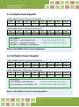
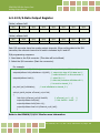
2.3.2 INT_CHAN_0/1
INT0/1
Inverted/Noninverted
select
(INV0/1)
Enable/Disable select
(EN0/1)
INT_CHAN_0/1
The architecture for INT_CHAN_0 and INT_CHAN_1 is shown in the above figure. The only
difference between INT0 and INT1 is that the INT_CHAN_0 signal source is from the 8254
counter0 output and the INT_CHAN_1 signal source is from the 8254 counter2 output.
INT_CHAN_0/1 must be fixed at a low level state normally and a high_pulse
generated to interrupt the PC.
EN0/1 can be used to enable/disable the INT_CHAN_0/1 in the following manner: (Refer to
Sec. 6.3.4)
EN0/1 = 0 INT_CHAN_0/1 = disabled
EN0/1 = 1 INT_CHAN_0/1 = enabled
INV0/1 can be used to invert/non-invert INT0/1 in the following manner: (Refer to Sec. 6.3.5)
INV0/1 = 0 INT_CHAN_0/1 = inverted state for INT0/1
INV0/1 = 1 INT_CHAN_0/1 = non-inverted state for INT0/1
As noted above, if INT\ is fixed at a low level state, the PEX-DA and
PIO/PISO-DAxU series will interrupt the PC continuously, so the interrupt service
routine should use INV0/1 to invert/non-invert the INT0/1 in order to generate a
high_pulse (Refer to the next section).

PEX/PIO/PISO-DA Series Card
Analog Output Boards
User Manual/ Ver. 3.1/ Oct. 2013/ PMH-0010-31/ Page: 17
2.3.3 Initial_High, Ative_Low Interrupt Source
If INT0 (8254 counter0 output) is an initial_high, active_low signal (depending on 8254
counter mode), the interrupt service routine should use INV0 to invert/non-invert INT0 to
generate a high_pulse in the following manner: (Refer to DEMO3.C)
Initial settings:
void interrupt irq_service()
{
if (now_int_state==1) /* now INT0 is changed to LOW */(a)
{ /* --> INT_CHAN_0=!INT0=HIGH now */
COUNT_L++; /* find a LOW_pulse (INT0) */
If((inport(wBase+7)&1)==0) /* the INT0 is still fixed in LOW */
{ /* need to generate a high_pulse */
outportb(wBase+0x2a,1); /* INV0 select the non-inverted input */(b)
/* INT_CHAN_0=INT0=LOW --> */
/* INT_CHAN_0 generate a high_pulse */
now_int_state=0; /* now INT0=LOW */
}
else now_int_state=1; /* now INT0=HIGH */
/* don’t have to generate high_pulse */
}
else /* now INT0 is changed to HIGH */(c)
{ /* --> INT_CHAN_0=INT0=HIGH now */
COUNT_H++; /* find a HIGH_pulse (INT0) */
If((inport(wBase+7)&1)==1) /* the INT0 is still fixed in HIGH */
{ /* need to generate a high_pulse */
outportb(wBase+0x2a,0); /* INV0 select the inverted input */(d)
/* INT_CHAN_0=!INT0=LOW --> */
/* INT_CHAN_0 generate a high_pulse */
now_int_state=1; /* now INT0=HIGH */
}
else now_int_state=0; /* now INT0=LOW */
/* don’t have to generate high_pulse */
}
if (wIrq>=8) outportb(A2_8259,0x20);
outportb(A1_8259,0x20);
}
INT0
INV0
INT_CHAN_0
(a) (b) (c) (d)
now_int_state=1; /* initial state for INT0 */
outportb(wBase+0x2a,0); /* select the inverted INT0 */

PEX/PIO/PISO-DA Series Card
Analog Output Boards
User Manual/ Ver. 3.1/ Oct. 2013/ PMH-0010-31/ Page: 18
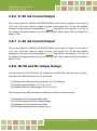
2.3.4 Initial_Low, Ative_High Interrupt Source
If INT0 (8254 counter0 output) is an initial_low, active_high signal (depending on the 8254
counter mode), the interrupt service routine should use INV0 to invert/non-invert INT0 to
generate a high_pulse in the following manner: (Refer to DEMO4.C)
Initial setting:
void interrupt irq_service()
{
if (now_int_state==1) /* now INT0 is changed to LOW */(c)
{ /* --> INT_CHAN_0=!INT0=HIGH now */
COUNT_L++; /* find a LOW_pulse (INT0) */
If((inport(wBase+7)&1)==0)/* the INT0 is still fixed in LOW */
{ /* need to generate a high_pulse */
outportb(wBase+0x2a,1); /* INV0 select the non-inverted input */(d)
/* INT_CHAN_0=INT0=LOW --> */
/* INT_CHAN_0 generate a high_pulse */
now_int_state=0; /* now INT0=LOW */
}
else now_int_state=1; /* now INT0=HIGH */
/* don’t have to generate high_pulse */
}
else /* now INT0 is changed to HIGH */(a)
{ /* --> INT_CHAN_0=INT0=HIGH now */
COUNT_H++; /* find a High_pulse (INT0) */
If((inport(wBase+7)&1)==1)/* the INT0 is still fixed in HIGH */
{ /* need to generate a high_pulse */
outportb(wBase+0x2a,0); /* INV0 select the inverted input */(b)
/* INT_CHAN_0=!INT0=LOW --> */
/* INT_CHAN_0 generate a high_pulse */
now_int_state=1; /* now INT0=HIGH */
}
else now_int_state=0; /* now INT0=LOW */
/* don’t have to generate high_pulse */
}
if (wIrq>=8) outportb(A2_8259,0x20);
outportb(A1_8259,0x20);
}
now_int_state=0; /* initial state for INT0 */
outportb(wBase+0x2a,1); /* select the non-inverted INT0 */
INT0
INV0
INT_CHAN_0
(a) (b) (c) (d)

PEX/PIO/PISO-DA Series Card
Analog Output Boards
User Manual/ Ver. 3.1/ Oct. 2013/ PMH-0010-31/ Page: 19
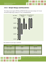
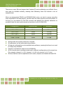
2.3.5 Multiple Interrupt Source
Assume: INT0 is initial Low and active High,
INT1 is initial High and active Low
as below:
Refer to DEMO5.C for the source program. All of these falling-edge and rising-edge can
be detected using DEMO5.C.
Note:
When the interrupt is active, the user program has to identify the active signals. These
signals may all be active at the same time, so the interrupt service routine has to service
all active signals at the same time.
INT0 and INT1
are active at
the same time
INT1
INT0
INT1 returns to
normal
INT0 and INT1
return to
normal at the
same time
INT1 is active

PEX/PIO/PISO-DA Series Card
Analog Output Boards
User Manual/ Ver. 3.1/ Oct. 2013/ PMH-0010-31/ Page: 20
/* ------------------------------------------------------------------------------------------------------- */
/* Note : 1.The hold_time of INT_CHAN_0 & INT_CHAN_1 must long */
/* enoug. */
/* 2.The ISR must read the interrupt status again to */
/* identify the active interrupt source. */
/* 3.The INT_CHAN_0 & INT_CHAN_1 can be active at the same */
/* time. */
/* --------------------------------------------------------------------------------------------------- */
void interrupt irq_service()
{
/* now ISR can not know which interrupt is active */
new_int_state=inportb(wBase+7)&0x03; /* read all interrupt */
/* signal state */
int_c=new_int_state^now_int_state; /* compare new_state to */
/* old_state */
if ((int_c&0x01)==1) /* INT_CHAN_0 is active */
{
if ((new_int_state&1)==0) /* INT0 change to low now */
{
INT0_L++;
}
else /* INT0 change to high now */
{
INT0_H++;
}
invert=invert^1; /* generate high_pulse */
}
if ((int_c&0x02)==2) /* INT_CHAN_1 is active */
{
if ((new_int_state&2)==0) /* INT1 change to low now */
{
INT1_L++;
}
else /* INT1 change to high now */
{
INT1_H++;
}
invert=invert^2; /* generate high_pulse */
}
now_int_state=new_int_state; /* update interrupt status */
outportb(wBase+0x2a,invert); /* generate a high pulse */
if (wIrq>=8) outportb(A2_8259,0x20);
outportb(A1_8259,0x20);
}
Page is loading ...
Page is loading ...
Page is loading ...
Page is loading ...
Page is loading ...
Page is loading ...
Page is loading ...
Page is loading ...
Page is loading ...
Page is loading ...
Page is loading ...
Page is loading ...
Page is loading ...
Page is loading ...
Page is loading ...
Page is loading ...
Page is loading ...
Page is loading ...
Page is loading ...
Page is loading ...
Page is loading ...
Page is loading ...
Page is loading ...
Page is loading ...
Page is loading ...
Page is loading ...
Page is loading ...
Page is loading ...
Page is loading ...
Page is loading ...
Page is loading ...
Page is loading ...
Page is loading ...
Page is loading ...
Page is loading ...
Page is loading ...
Page is loading ...
Page is loading ...
Page is loading ...
Page is loading ...
Page is loading ...
Page is loading ...
Page is loading ...
Page is loading ...
Page is loading ...
Page is loading ...
Page is loading ...
Page is loading ...
Page is loading ...
Page is loading ...
Page is loading ...
Page is loading ...
Page is loading ...
Page is loading ...
Page is loading ...
Page is loading ...
-
 1
1
-
 2
2
-
 3
3
-
 4
4
-
 5
5
-
 6
6
-
 7
7
-
 8
8
-
 9
9
-
 10
10
-
 11
11
-
 12
12
-
 13
13
-
 14
14
-
 15
15
-
 16
16
-
 17
17
-
 18
18
-
 19
19
-
 20
20
-
 21
21
-
 22
22
-
 23
23
-
 24
24
-
 25
25
-
 26
26
-
 27
27
-
 28
28
-
 29
29
-
 30
30
-
 31
31
-
 32
32
-
 33
33
-
 34
34
-
 35
35
-
 36
36
-
 37
37
-
 38
38
-
 39
39
-
 40
40
-
 41
41
-
 42
42
-
 43
43
-
 44
44
-
 45
45
-
 46
46
-
 47
47
-
 48
48
-
 49
49
-
 50
50
-
 51
51
-
 52
52
-
 53
53
-
 54
54
-
 55
55
-
 56
56
-
 57
57
-
 58
58
-
 59
59
-
 60
60
-
 61
61
-
 62
62
-
 63
63
-
 64
64
-
 65
65
-
 66
66
-
 67
67
-
 68
68
-
 69
69
-
 70
70
-
 71
71
-
 72
72
-
 73
73
-
 74
74
-
 75
75
-
 76
76


ICP PEX-DA4 User manual
- Category
- Motherboards
- Type
- User manual
Ask a question and I''ll find the answer in the document
Finding information in a document is now easier with AI
Related papers
Other documents
-
Omega OME-PISO-813 Owner's manual
-
-
-
Omega Engineering OME-PIO-D96 User manual
-
-
-
 Baldor-Reliance Series 5 Inverter : Open Chassis Mount - Single Phase Input Owner's manual
-
Extron P/2 DA8 User manual
-
Omega OME-PCI-1002 User manual
-
Savant AMP-8125-00 Deployment Guide
