


IMPORTANT NOTICE
Texas Instruments and its subsidiaries (TI) reserve the right to make changes to their products or to discontinue
any product or service without notice, and advise customers to obtain the latest version of relevant information
to verify, before placing orders, that information being relied on is current and complete. All products are sold
subject to the terms and conditions of sale supplied at the time of order acknowledgment, including those
pertaining to warranty, patent infringement, and limitation of liability.
TI warrants performance of its semiconductor products to the specifications applicable at the time of sale in
accordance with TI’s standard warranty. Testing and other quality control techniques are utilized to the extent
TI deems necessary to support this warranty. Specific testing of all parameters of each device is not necessarily
performed, except those mandated by government requirements.
Customers are responsible for their applications using TI components.
In order to minimize risks associated with the customer’s applications, adequate design and operating
safeguards must be provided by the customer to minimize inherent or procedural hazards.
TI assumes no liability for applications assistance or customer product design. TI does not warrant or represent
that any license, either express or implied, is granted under any patent right, copyright, mask work right, or other
intellectual property right of TI covering or relating to any combination, machine, or process in which such
semiconductor products or services might be or are used. TI’s publication of information regarding any third
party’s products or services does not constitute TI’s approval, warranty or endorsement thereof.
Copyright 2000, Texas Instruments Incorporated

iii
Contents
Section Title Page
1 Introduction 1–1. . . . . . . . . . . . . . . . . . . . . . . . . . . . . . . . . . . . . . . . . . . . . . . . . . . . . .
1.1 Description 1–1. . . . . . . . . . . . . . . . . . . . . . . . . . . . . . . . . . . . . . . . . . . . . . . . .
1.2 Features 1–1. . . . . . . . . . . . . . . . . . . . . . . . . . . . . . . . . . . . . . . . . . . . . . . . . . .
1.3 Related Documents 1–2. . . . . . . . . . . . . . . . . . . . . . . . . . . . . . . . . . . . . . . . . .
1.4 Ordering Information 1–2. . . . . . . . . . . . . . . . . . . . . . . . . . . . . . . . . . . . . . . . .
2 Terminal Descriptions 2–1. . . . . . . . . . . . . . . . . . . . . . . . . . . . . . . . . . . . . . . . . . . . .
3 TSB12LV26 Controller Programming Model 3–1. . . . . . . . . . . . . . . . . . . . . . . . .
3.1 PCI Configuration Registers 3–3. . . . . . . . . . . . . . . . . . . . . . . . . . . . . . . . . .
3.2 Vendor ID Register 3–3. . . . . . . . . . . . . . . . . . . . . . . . . . . . . . . . . . . . . . . . . .
3.3 Device ID Register 3–4. . . . . . . . . . . . . . . . . . . . . . . . . . . . . . . . . . . . . . . . . . .
3.4 Command Register 3–4. . . . . . . . . . . . . . . . . . . . . . . . . . . . . . . . . . . . . . . . . .
3.5 Status Register 3–5. . . . . . . . . . . . . . . . . . . . . . . . . . . . . . . . . . . . . . . . . . . . . .
3.6 Class Code and Revision ID Register 3–6. . . . . . . . . . . . . . . . . . . . . . . . . .
3.7 Latency Timer and Class Cache Line Size Register 3–6. . . . . . . . . . . . . .
3.8 Header Type and BIST Register 3–7. . . . . . . . . . . . . . . . . . . . . . . . . . . . . . .
3.9 OHCI Base Address Register 3–7. . . . . . . . . . . . . . . . . . . . . . . . . . . . . . . . .
3.10 TI Extension Base Address Register 3–8. . . . . . . . . . . . . . . . . . . . . . . . . . .
3.11 Subsystem Identification Register 3–8. . . . . . . . . . . . . . . . . . . . . . . . . . . . .
3.12 Power Management Capabilities Pointer Register 3–9. . . . . . . . . . . . . . .
3.13 Interrupt Line and Pin Register 3–9. . . . . . . . . . . . . . . . . . . . . . . . . . . . . . . .
3.14 MIN_GNT and MAX_LAT Register 3–10. . . . . . . . . . . . . . . . . . . . . . . . . . . . .
3.15 OHCI Control Register 3–10. . . . . . . . . . . . . . . . . . . . . . . . . . . . . . . . . . . . . . .
3.16 Capability ID and Next Item Pointer Register 3–11. . . . . . . . . . . . . . . . . . . .
3.17 Power Management Capabilities Register 3–12. . . . . . . . . . . . . . . . . . . . . .
3.18 Power Management Control and Status Register 3–13. . . . . . . . . . . . . . . .
3.19 Power Management Extension Register 3–13. . . . . . . . . . . . . . . . . . . . . . . .
3.20 Miscellaneous Configuration Register 3–14. . . . . . . . . . . . . . . . . . . . . . . . . .
3.21 Link Enhancement Control Register 3–15. . . . . . . . . . . . . . . . . . . . . . . . . . . .
3.22 Subsystem Access Register 3–16. . . . . . . . . . . . . . . . . . . . . . . . . . . . . . . . . .
3.23 GPIO Control Register 3–17. . . . . . . . . . . . . . . . . . . . . . . . . . . . . . . . . . . . . . .
4 OHCI Registers 4–1. . . . . . . . . . . . . . . . . . . . . . . . . . . . . . . . . . . . . . . . . . . . . . . . . . .
4.1 OHCI Version Register 4–4. . . . . . . . . . . . . . . . . . . . . . . . . . . . . . . . . . . . . . .
4.2 GUID ROM Register 4–5. . . . . . . . . . . . . . . . . . . . . . . . . . . . . . . . . . . . . . . . .
4.3 Asynchronous Transmit Retries Register 4–6. . . . . . . . . . . . . . . . . . . . . . .
4.4 CSR Data Register 4–6. . . . . . . . . . . . . . . . . . . . . . . . . . . . . . . . . . . . . . . . . .
4.5 CSR Compare Register 4–7. . . . . . . . . . . . . . . . . . . . . . . . . . . . . . . . . . . . . .
4.6 CSR Control Register 4–7. . . . . . . . . . . . . . . . . . . . . . . . . . . . . . . . . . . . . . . .

iv
4.7 Configuration ROM Header Register 4–8. . . . . . . . . . . . . . . . . . . . . . . . . . .
4.8 Bus Identification Register 4–8. . . . . . . . . . . . . . . . . . . . . . . . . . . . . . . . . . . .
4.9 Bus Options Register 4–9. . . . . . . . . . . . . . . . . . . . . . . . . . . . . . . . . . . . . . . .
4.10 GUID High Register 4–10. . . . . . . . . . . . . . . . . . . . . . . . . . . . . . . . . . . . . . . . . .
4.11 GUID Low Register 4–10. . . . . . . . . . . . . . . . . . . . . . . . . . . . . . . . . . . . . . . . . .
4.12 Configuration ROM Mapping Register 4–11. . . . . . . . . . . . . . . . . . . . . . . . . .
4.13 Posted Write Address Low Register 4–11. . . . . . . . . . . . . . . . . . . . . . . . . . . .
4.14 Posted Write Address High Register 4–12. . . . . . . . . . . . . . . . . . . . . . . . . . .
4.15 Vendor ID Register 4–12. . . . . . . . . . . . . . . . . . . . . . . . . . . . . . . . . . . . . . . . . .
4.16 Host Controller Control Register 4–13. . . . . . . . . . . . . . . . . . . . . . . . . . . . . . .
4.17 Self-ID Buffer Pointer Register 4–14. . . . . . . . . . . . . . . . . . . . . . . . . . . . . . . .
4.18 Self-ID Count Register 4–14. . . . . . . . . . . . . . . . . . . . . . . . . . . . . . . . . . . . . . .
4.19 Isochronous Receive Channel Mask High Register 4–15. . . . . . . . . . . . . .
4.20 Isochronous Receive Channel Mask Low Register 4–16. . . . . . . . . . . . . . .
4.21 Interrupt Event Register 4–17. . . . . . . . . . . . . . . . . . . . . . . . . . . . . . . . . . . . . .
4.22 Interrupt Mask Register 4–19. . . . . . . . . . . . . . . . . . . . . . . . . . . . . . . . . . . . . .
4.23 Isochronous Transmit Interrupt Event Register 4–20. . . . . . . . . . . . . . . . . .
4.24 Isochronous Transmit Interrupt Mask Register 4–21. . . . . . . . . . . . . . . . . . .
4.25 Isochronous Receive Interrupt Event Register 4–22. . . . . . . . . . . . . . . . . . .
4.26 Isochronous Receive Interrupt Mask Register 4–22. . . . . . . . . . . . . . . . . . .
4.27 Fairness Control Register 4–23. . . . . . . . . . . . . . . . . . . . . . . . . . . . . . . . . . . .
4.28 Link Control Register 4–24. . . . . . . . . . . . . . . . . . . . . . . . . . . . . . . . . . . . . . . . .
4.29 Node Identification Register 4–25. . . . . . . . . . . . . . . . . . . . . . . . . . . . . . . . . . .
4.30 PHY Layer Control Register 4–26. . . . . . . . . . . . . . . . . . . . . . . . . . . . . . . . . . .
4.31 Isochronous Cycle Timer Register 4–27. . . . . . . . . . . . . . . . . . . . . . . . . . . . .
4.32 Asynchronous Request Filter High Register 4–28. . . . . . . . . . . . . . . . . . . . .
4.33 Asynchronous Request Filter Low Register 4–30. . . . . . . . . . . . . . . . . . . . .
4.34 Physical Request Filter High Register 4–31. . . . . . . . . . . . . . . . . . . . . . . . . .
4.35 Physical Request Filter Low Register 4–33. . . . . . . . . . . . . . . . . . . . . . . . . .
4.36 Physical Upper Bound Register (Optional Register) 4–34. . . . . . . . . . . . . .
4.37 Asynchronous Context Control Register 4–35. . . . . . . . . . . . . . . . . . . . . . . .
4.38 Asynchronous Context Command Pointer Register 4–36. . . . . . . . . . . . . .
4.39 Isochronous Transmit Context Control Register 4–37. . . . . . . . . . . . . . . . . .
4.40 Isochronous Transmit Context Command Pointer Register 4–38. . . . . . . .
4.41 Isochronous Receive Context Control Register 4–38. . . . . . . . . . . . . . . . . .
4.42 Isochronous Receive Context Command Pointer Register 4–40. . . . . . . .
4.43 Isochronous Receive Context Match Register 4–41. . . . . . . . . . . . . . . . . . .
5 GPIO Interface 5–1. . . . . . . . . . . . . . . . . . . . . . . . . . . . . . . . . . . . . . . . . . . . . . . . . . . .
6 Serial ROM Interface 6–1. . . . . . . . . . . . . . . . . . . . . . . . . . . . . . . . . . . . . . . . . . . . . .
7 Electrical Characteristics 7–1. . . . . . . . . . . . . . . . . . . . . . . . . . . . . . . . . . . . . . . . . .
7.1 Absolute Maximum Ratings Over Operating Temperature Ranges 7–1.
7.2 Recommended Operating Conditions 7–2. . . . . . . . . . . . . . . . . . . . . . . . . .
7.3 Electrical Characteristics Over Recommended Operating Conditions 7–3
7.4 Switching Characteristics for PCI Interface 7–3. . . . . . . . . . . . . . . . . . . . . .


vi
List of Illustrations
Figure Title Page
2–1 Terminal Assignments 2–1. . . . . . . . . . . . . . . . . . . . . . . . . . . . . . . . . . . . . . . . . . .
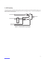
3–1 TSB12LV26 Block Diagram 3–2. . . . . . . . . . . . . . . . . . . . . . . . . . . . . . . . . . . . . .
5–1 GPIO2 and GPIO3 Logic Diagram 5–1. . . . . . . . . . . . . . . . . . . . . . . . . . . . . . . .

vii
List of Tables
Table Title Page
2–1 Signals Sorted by Terminal Number 2–2. . . . . . . . . . . . . . . . . . . . . . . . . . . . . . .
2–2 Signal Names Sorted Alphanumerically to Terminal Number 2–3. . . . . . . . . .
2–3 Power Supply Terminals 2–3. . . . . . . . . . . . . . . . . . . . . . . . . . . . . . . . . . . . . . . . .
2–4 PCI System Terminals 2–4. . . . . . . . . . . . . . . . . . . . . . . . . . . . . . . . . . . . . . . . . . .
2–5 PCI Address and Data Terminals 2–5. . . . . . . . . . . . . . . . . . . . . . . . . . . . . . . . .
2–6 PCI Interface Control Terminals 2–6. . . . . . . . . . . . . . . . . . . . . . . . . . . . . . . . . . .
2–7 IEEE 1394 PHY/Link Terminals 2–7. . . . . . . . . . . . . . . . . . . . . . . . . . . . . . . . . . .
2–8 Miscellaneous Terminals 2–7. . . . . . . . . . . . . . . . . . . . . . . . . . . . . . . . . . . . . . . . .
3–1 Bit Field Access Tag Descriptions 3–1. . . . . . . . . . . . . . . . . . . . . . . . . . . . . . . . .
3–2 PCI Configuration Register Map 3–3. . . . . . . . . . . . . . . . . . . . . . . . . . . . . . . . . .
3–3 Command Register Description 3–4. . . . . . . . . . . . . . . . . . . . . . . . . . . . . . . . . . .
3–4 Status Register Description 3–5. . . . . . . . . . . . . . . . . . . . . . . . . . . . . . . . . . . . . .
3–5 Class Code and Revision ID Register Description 3–6. . . . . . . . . . . . . . . . . . .
3–6 Latency Timer and Class Cache Line Size Register Description 3–6. . . . . . .
3–7 Header Type and BIST Register Description 3–7. . . . . . . . . . . . . . . . . . . . . . . .
3–8 OHCI Base Address Register Description 3–7. . . . . . . . . . . . . . . . . . . . . . . . . .
3–9 Subsystem Identification Register Description 3–8. . . . . . . . . . . . . . . . . . . . . .
3–10 Interrupt Line and Pin Register Description 3–9. . . . . . . . . . . . . . . . . . . . . . . . .
3–11 MIN_GNT and MAX_LAT Register Description 3–10. . . . . . . . . . . . . . . . . . . . .
3–12 OHCI Control Register Description 3–10. . . . . . . . . . . . . . . . . . . . . . . . . . . . . . . .
3–13 Capability ID and Next Item Pointer Register Description 3–11. . . . . . . . . . . . .
3–14 Power Management Capabilities Register Description 3–12. . . . . . . . . . . . . . .
3–15 Power Management Control and Status Register Description 3–13. . . . . . . . .
3–16 Power Management Extension Register Description 3–13. . . . . . . . . . . . . . . . .
3–17 Miscellaneous Configuration Register 3–14. . . . . . . . . . . . . . . . . . . . . . . . . . . . .
3–18 Link Enhancement Control Register Description 3–15. . . . . . . . . . . . . . . . . . . .
3–19 Subsystem Access Register Description 3–16. . . . . . . . . . . . . . . . . . . . . . . . . . .
3–20 GPIO Control Register Description 3–17. . . . . . . . . . . . . . . . . . . . . . . . . . . . . . . .
4–1 OHCI Register Map 4–1. . . . . . . . . . . . . . . . . . . . . . . . . . . . . . . . . . . . . . . . . . . . .
4–2 OHCI Version Register Description 4–4. . . . . . . . . . . . . . . . . . . . . . . . . . . . . . . .
4–3 GUID ROM Register Description 4–5. . . . . . . . . . . . . . . . . . . . . . . . . . . . . . . . . .
4–4 Asynchronous Transmit Retries Register Description 4–6. . . . . . . . . . . . . . . .
4–5 CSR Control Register Description 4–7. . . . . . . . . . . . . . . . . . . . . . . . . . . . . . . . .
4–6 Configuration ROM Header Register Description 4–8. . . . . . . . . . . . . . . . . . . .
4–7 Bus Options Register Description 4–9. . . . . . . . . . . . . . . . . . . . . . . . . . . . . . . . .
4–8 Configuration ROM Mapping Register Description 4–11. . . . . . . . . . . . . . . . . . .
4–9 Posted Write Address High Register Description 4–12. . . . . . . . . . . . . . . . . . . .

viii
4–10 Host Controller Control Register Description 4–13. . . . . . . . . . . . . . . . . . . . . . . .
4–11 Self-ID Count Register Description 4–14. . . . . . . . . . . . . . . . . . . . . . . . . . . . . . . .
4–12 Isochronous Receive Channel Mask High Register Description 4–15. . . . . . .
4–13 Isochronous Receive Channel Mask Low Register Description 4–16. . . . . . . .
4–14 Interrupt Event Register Description 4–17. . . . . . . . . . . . . . . . . . . . . . . . . . . . . . .
4–15 Interrupt Mask Register Description 4–19. . . . . . . . . . . . . . . . . . . . . . . . . . . . . . .
4–16 Isochronous Transmit Interrupt Event Register Description 4–20. . . . . . . . . . .
4–17 Isochronous Receive Interrupt Event Register Description 4–22. . . . . . . . . . .
4–18 Fairness Control Register Description 4–23. . . . . . . . . . . . . . . . . . . . . . . . . . . . .
4–19 Link Control Register Description 4–24. . . . . . . . . . . . . . . . . . . . . . . . . . . . . . . . .
4–20 Node Identification Register Description 4–25. . . . . . . . . . . . . . . . . . . . . . . . . . .
4–21 PHY Control Register Description 4–26. . . . . . . . . . . . . . . . . . . . . . . . . . . . . . . . .
4–22 Isochronous Cycle Timer Register Description 4–27. . . . . . . . . . . . . . . . . . . . . .
4–23 Asynchronous Request Filter High Register Description 4–28. . . . . . . . . . . . .
4–24 Asynchronous Request Filter Low Register Description 4–30. . . . . . . . . . . . . .
4–25 Physical Request Filter High Register Description 4–31. . . . . . . . . . . . . . . . . . .
4–26 Physical Request Filter Low Register Description 4–33. . . . . . . . . . . . . . . . . . .
4–27 Asynchronous Context Control Register Description 4–35. . . . . . . . . . . . . . . . .
4–28 Asynchronous Context Command Pointer Register Description 4–36. . . . . . .
4–29 Isochronous Transmit Context Control Register Description 4–37. . . . . . . . . .
4–30 Isochronous Receive Context Control Register Description 4–38. . . . . . . . . . .
4–31 Isochronous Receive Context Match Register Description 4–41. . . . . . . . . . . .
6–1 Registers and Bits Loadable through Serial ROM 6–1. . . . . . . . . . . . . . . . . . .
6–2 Serial ROM Map 6–2. . . . . . . . . . . . . . . . . . . . . . . . . . . . . . . . . . . . . . . . . . . . . . . .

1–1
1 Introduction
1.1 Description
The Texas Instruments TSB12LV26 is a PCI-to-1394 host controller compatible with the latest
PCI Local Bus
,
PCI
Bus Power Management Interface
, IEEE 1394-1995, and
1394 Open Host Controller Interface Specification
. The
chip provides the IEEE 1394 link function, and is compatible with serial bus data rates of 100 Mbits/s, 200 Mbits/s,
and 400 Mbits/s.
As required by the
1394 Open Host Controller Interface Specification
(OHCI)
and IEEE proposal 1394a specification,
internal control registers are memory-mapped and nonprefetchable. The PCI configuration header is accessed
through configuration cycles specified by PCI, and provides Plug-and-Play (PnP) compatibility. Furthermore, the
TSB12LV26 is compliant with the
PCI Bus Power Management Interface Specification
, per the
PC 99 Design Guide
requirements. TSB12LV26 supports the D0, D2, and D3 power states.
The TSB12LV26 design provides PCI bus master bursting, and is capable of transferring a cacheline of data at
132 Mbytes/s after connection to the memory controller. Since PCI latency can be large, deep FIFOs are provided
to buffer 1394 data.
The TSB12LV26 provides physical write posting buffers and a highly tuned physical data path for SBP-2 performance.
The TSB12LV26 also provides multiple isochronous contexts, multiple cacheline burst transfers, advanced internal
arbitration, and bus holding buffers on the PHY/link interface.
An advanced CMOS process is used to achieve low power consumption while operating at PCI clock rates up to
33 MHz.
1.2 Features
The TSB12LV26 supports the following features:
•3.3-V core logic with universal PCI interfaces compatible with 3.3-V and 5-V PCI signaling environments
•Serial bus data rates of 100, 200, and 400 Mbits/s
•Provides bus-hold buffers on physical interface for low-cost single capacitor isolation
•Physical write posting of up to three outstanding transactions
•Serial ROM interface supports 2-wire devices
•External cycle timer control for customized synchronization
•Implements PCI burst transfers and deep FIFOs to tolerate large host latency
•Provides two general-purpose I/Os
•Fabricated in advanced low-power CMOS process
•Packaged in 100-terminal LQFP (PZ)
•Supports PCI_CLKRUN protocol

1–2
1.3 Related Documents
•
1394 Open Host Controller Interface Specification 1.0
•
P1394 Standard for a High Performance Serial Bus
(IEEE 1394-1995)
•
P1394a Draft Standard for a High Performance Serial Bus (Supplement)
•
PC 99 Design Guide
•
PCI Bus Power Management Interface Specification (Revision 1.0)
•
PCI Local Bus Specification (Revision 2.2)
•
Serial Bus Protocol 2
(SBP–2)
1.4 Ordering Information
ORDERING NUMBER NAME VOLTAGE PACKAGE
TSB12LV26 OHCI-Lynx PCI-Based IEEE 1394 Host Controller 3.3V-, 5V-Tolerant I/Os 100-Terminal LQFP

2–1
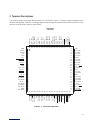
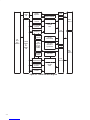
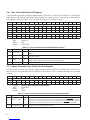
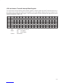
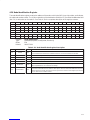
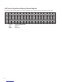
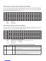
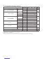
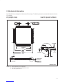
2 Terminal Descriptions
This section provides the terminal descriptions for the TSB12LV26. Figure 2–1 shows the signal assigned to each
terminal in the package. Table 2–1 is a listing of signal names arranged in terminal number order, and Table 2–2 lists
terminals in alphanumeric order by signal names.
1
2
3
4
5
6
7
8
9
10
11
12
13
14
15
16
17
18
19
20
21
22
23
24
25
76
77
78
79
80
81
82
83
84
85
86
87
88
89
90
91
92
93
94
95
96
97
98
99
100
75
74
73
72
71
70
69
68
67
66
65
64
63
62
61
60
59
58
57
56
55
54
53
52
51
50
49
48
47
46
45
44
43
42
41
40
39
38
37
36
35
34
33
32
31
30
29
28
27
26 REG18
PHY_SCLK
GND
PHY_DATA1
PHY_DATA2
PHY_DATA5
GND
PHY_DATA6
PHY_DATA7
PCI_AD25
PCI_AD24
PCI_C/BE3
PCI_IDSEL
GND
PCI_AD18
PCI_AD17
PCI_AD16
GND
REG18
PZ PACKAGE
(TOP VIEW)
PHY_DATA0
PCI_AD21
PHY_LREQ
PHY_DATA3
PHY_DATA4
PCI_AD19
GPIO2
GPIO3
SCL
SDA
VCCP
PCI_CLKRUN
PCI_INTA
3.3 VCC
G_RST
GND
PCI_CLK
PCI_GNT
VCCP
PCI_AD30
3.3 VCC
PCI_AD29
PCI_AD28
PCI_AD27
GND
PCI_AD26
3.3 VCC
PCI_REQ
PCI_PME
PCI_AD31
GND GND
PCI_AD1
PCI_AD2
3.3 VCC
PCI_AD5
PCI_AD7
PCI_AD8
PCI_AD9
GND
PCI_AD12
PCI_AD14
PCI_AD15
PCI_C/BE1
PCI_AD0
PCI_AD3
PCI_AD4
PCI_AD6
PCI_C/BE0
VCCP
PCI_AD10
PCI_AD11
PCI_AD13
3.3 VCC
PCI_PAR
PCI_SERR
PCI_RST
CYCLEOUT
CYCLEIN
REG_EN
CCP
V
CC
3.3 V
PHY_CTL1
PHY_CTL0
CC
3.3 V
PHY_LINKON
PHY_LPS
PCI_AD22
PCI_AD23
PCI_AD20
CCP
V
PCI_C/BE2
PCI_FRAME
PCI_IRDY
PCI_TRDY
PCI_DEVSEL
PCI_STOP
PCI_PERR
CC
3.3 V
CC
3.3 V
CC
3.3 V
Figure 2–1. Terminal Assignments

2–2
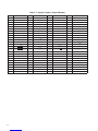
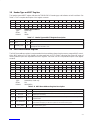
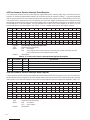
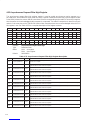
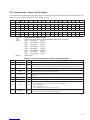
Table 2–1. Signals Sorted by Terminal Number
NO. TERMINAL NAME NO. TERMINAL NAME NO. TERMINAL NAME NO. TERMINAL NAME
1 GND 26 PCI_AD25 51 PCI_SERR 76 PCI_RST
2 GPIO2 27 PCI_AD24 52 PCI_PAR 77 CYCLEOUT
3 GPIO3 28 PCI_C/BE3 53 PCI_C/BE1 78 CYCLEIN
4 SCL 29 PCI_IDSEL 54 PCI_AD15 79 REG_EN
5 SDA 30 GND 55 3.3 VCC 80 3.3 VCC
6 VCCP 31 PCI_AD23 56 PCI_AD14 81 PHY_DATA7
7 PCI_CLKRUN 32 PCI_AD22 57 PCI_AD13 82 PHY_DATA6
8 PCI_INTA 33 PCI_AD21 58 PCI_AD12 83 GND
93.3 VCC 34 PCI_AD20 59 PCI_AD11 84 PHY_DATA5
10 G_RST 35 3.3 VCC 60 GND 85 PHY_DATA4
11 GND 36 PCI_AD19 61 PCI_AD10 86 PHY_DATA3
12 PCI_CLK 37 PCI_AD18 62 PCI_AD9 87 VCCP
13 3.3 VCC 38 PCI_AD17 63 VCCP 88 PHY_DATA2
14 PCI_GNT 39 VCCP 64 PCI_AD8 89 PHY_DATA1
15 PCI_REQ 40 PCI_AD16 65 PCI_C/BE0 90 PHY_DATA0
16 VCCP 41 PCI_C/BE2 66 PCI_AD7 91 3.3 VCC
17 PCI_PME 42 REG18 67 PCI_AD6 92 PHY_CTL1
18 PCI_AD31 43 PCI_FRAME 68 PCI_AD5 93 PHY_CTL0
19 PCI_AD30 44 PCI_IRDY 69 PCI_AD4 94 GND
20 3.3 VCC 45 PCI_TRDY 70 3.3 VCC 95 PHY_SCLK
21 PCI_AD29 46 3.3 VCC 71 PCI_AD3 96 3.3 VCC
22 PCI_AD28 47 PCI_DEVSEL 72 PCI_AD2 97 PHY_LREQ
23 PCI_AD27 48 PCI_STOP 73 PCI_AD1 98 PHY_LINKON
24 GND 49 PCI_PERR 74 PCI_AD0 99 PHY_LPS
25 PCI_AD26 50 GND 75 GND 100 REG18

2–3
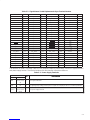
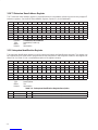
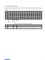
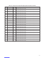
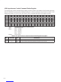
Table 2–2. Signal Names Sorted Alphanumerically to Terminal Number
TERMINAL NAME NO. TERMINAL NAME NO. TERMINAL NAME NO. TERMINAL NAME NO.
CYCLEIN 78 PCI_AD11 59 PCI_CLK 12 PHY_DATA7 81
CYCLEOUT 77 PCI_AD12 58 PCI_CLKRUN 7 PHY_LINKON 98
GND 1 PCI_AD13 57 PCI_DEVSEL 47 PHY_LPS 99
GND 11 PCI_AD14 56 PCI_FRAME 43 PHY_LREQ 97
GND 24 PCI_AD15 54 PCI_GNT 14 PHY_SCLK 95
GND 30 PCI_AD16 40 PCI_IDSEL 29 REG_EN 79
GND 50 PCI_AD17 38 PCI_INTA 8 REG18 42
GND 60 PCI_AD18 37 PCI_IRDY 44 REG18 100
GND 75 PCI_AD19 36 PCI_PAR 52 SCL 4
GND 83 PCI_AD20 34 PCI_PERR 49 SDA 5
GND 94 PCI_AD21 33 PCI_PME 17 VCCP 6
GPIO2 2 PCI_AD22 32 PCI_REQ 15 VCCP 16
GPIO3 3 PCI_AD23 31 PCI_RST 76 VCCP 39
G_RST 10 PCI_AD24 27 PCI_SERR 51 VCCP 63
PCI_AD0 74 PCI_AD25 26 PCI_STOP 48 VCCP 87
PCI_AD1 73 PCI_AD26 25 PCI_TRDY 45 3.3 VCC 9
PCI_AD2 72 PCI_AD27 23 PHY_CTL0 93 3.3 VCC 13
PCI_AD3 71 PCI_AD28 22 PHY_CTL1 92 3.3 VCC 20
PCI_AD4 69 PCI_AD29 21 PHY_DATA0 90 3.3 VCC 35
PCI_AD5 68 PCI_AD30 19 PHY_DATA1 89 3.3 VCC 46
PCI_AD6 67 PCI_AD31 18 PHY_DATA2 88 3.3 VCC 55
PCI_AD7 66 PCI_C/BE0 65 PHY_DATA3 86 3.3 VCC 70
PCI_AD8 64 PCI_C/BE1 53 PHY_DATA4 85 3.3 VCC 80
PCI_AD9 62 PCI_C/BE2 41 PHY_DATA5 84 3.3 VCC 91
PCI_AD10 61 PCI_C/BE3 28 PHY_DATA6 82 3.3 VCC 96
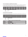
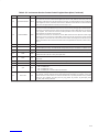
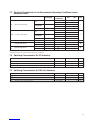
The terminals in Table 2–3 through Table 2–8 are grouped in tables by functionality, such as PCI system function
and power supply function. The terminal numbers are also listed for convenient reference.
Table 2–3. Power Supply Terminals
TERMINAL
I/O
DESCRIPTION
NAME NO.
I/O
DESCRIPTION
GND 1, 11, 24, 30,
50, 60, 75, 83,
94 IDevice ground terminals
VCCP 6, 16, 39, 63,
87 IPCI signaling clamp voltage power input. PCI signals are clamped per the
PCI Local Bus Specification
.
3.3 VCC 9, 13, 20, 35,
46, 55, 70, 80,
91, 96 I3.3-V power supply terminals

2–4
Table 2–4. PCI System Terminals
TERMINAL
I/O
DESCRIPTION
NAME NO.
I/O
DESCRIPTION
G_RST 10 I
Global power reset. This reset brings all of the TSB12LV26 internal registers to their default states, including
those registers not reset by PCI_RST. When G_RST is asserted, the device is completely nonfunctional.
When implementing wake capabilities from the 1394 host controller, it is necessary to implement two resets
to the TSB12LV26. G_RST should be a one-time power-on reset, and PCI_RST should be connected to the
PCI bus RST. If wake capabilities are not required, G_RST may be connected to the PCI bus RST (see
PCI_RST, terminal 76).
PCI_CLK 12 IPCI bus clock. Provides timing for all transactions on the PCI bus. All PCI signals are sampled at rising edge
of PCI_CLK.
PCI_INTA 8 O Interrupt signal. This output indicates interrupts from the TSB12LV26 to the host. This terminal is implemented
as open-drain.
PCI_RST 76 I
PCI reset. When this bus reset is asserted, the TSB12LV26 places all output buffers in a high impedance state
and resets all internal registers except device power management context- and vendor-specific bits initialized
by host power-on software. When PCI_RST is asserted, the device is completely nonfunctional.
If this terminal is implemented, then it should be connected to the PCI bus RST signal. Otherwise, it should
be pulled high to link VCC through a 4.7-kΩ resistor, or strapped to the G_RST terminal (see G_RST, terminal
10).

2–5
Table 2–5. PCI Address and Data Terminals
TERMINAL
I/O
DESCRIPTION
NAME NO.
I/O
DESCRIPTION
PCI_AD31
PCI_AD30
PCI_AD29
PCI_AD28
PCI_AD27
PCI_AD26
PCI_AD25
PCI_AD24
PCI_AD23
PCI_AD22
PCI_AD21
PCI_AD20
PCI_AD19
PCI_AD18
PCI_AD17
PCI_AD16
PCI_AD15
PCI_AD14
PCI_AD13
PCI_AD12
PCI_AD11
PCI_AD10
PCI_AD9
PCI_AD8
PCI_AD7
PCI_AD6
PCI_AD5
PCI_AD4
PCI_AD3
PCI_AD2
PCI_AD1
PCI_AD0
18
19
21
22
23
25
26
27
31
32
33
34
36
37
38
40
54
56
57
58
59
61
62
64
66
67
68
69
71
72
73
74
I/O PCI address/data bus. These signals make up the multiplexed PCI address and data bus on the PCI interface.
During the address phase of a PCI cycle, AD31–AD0 contain a 32-bit address or other destination information.
During the data phase, AD31–AD0 contain data.

2–6
Table 2–6. PCI Interface Control Terminals
TERMINAL
I/O
DESCRIPTION
NAME NO.
I/O
DESCRIPTION
PCI_C/BE0
PCI_C/BE1
PCI_C/BE2
PCI_C/BE3
65
53
41
28
I/O PCI bus commands and byte enables. The command and byte enable signals are multiplexed on the same PCI
terminals. During the address phase of a bus cycle PCI_C/BE3–PCI_C/BE0 defines the bus command. During
the data phase, this 4-bit bus is used as byte enables.
PCI_CLKRUN 7 I/O Clock run. This terminal provides clock control through the PCI_CLKRUN protocol. An internal pulldown
resistor is implemented on this terminal.
This terminal is implemented as open-drain.
PCI_DEVSEL 47 I/O PCI device select. The TSB12LV26 asserts this signal to claim a PCI cycle as the target device. As a PCI
initiator, the TSB12LV26 monitors this signal until a target responds. If no target responds before time-out
occurs, then the TSB12LV26 terminates the cycle with an initiator abort.
PCI_FRAME 43 I/O PCI cycle frame. This signal is driven by the initiator of a PCI bus cycle. PCI_FRAME is asserted to indicate
that a bus transaction is beginning, and data transfers continue while this signal is asserted. When PCI_FRAME
is deasserted, the PCI bus transaction is in the final data phase.
PCI_GNT 14 IPCI bus grant. This signal is driven by the PCI bus arbiter to grant the TSB12LV26 access to the PCI bus after
the current data transaction has completed. This signal may or may not follow a PCI bus request, depending
upon the PCI bus parking algorithm.
PCI_IDSEL 29 IInitialization device select. IDSEL selects the TSB12LV26 during configuration space accesses. IDSEL can be
connected to one of the upper 24 PCI address lines on the PCI bus.
PCI_IRDY 44 I/O PCI initiator ready. IRDY indicates the ability of the PCI bus initiator to complete the current data phase of the
transaction. A data phase is completed upon a rising edge of PCLK where both PCI_IRDY and PCI_TRDY are
asserted.
PCI_PAR 52 I/O
PCI parity. In all PCI bus read and write cycles, the TSB12LV26 calculates even parity across the AD and C/BE
buses. As an initiator during PCI cycles, the TSB12LV26 outputs this parity indicator with a one PCI_CLK delay.
As a target during PCI cycles, the calculated parity is compared to the initiator parity indicator; a miscompare
can result in a parity error assertion (PCI_PERR).
PCI_PERR 49 I/O PCI parity error indicator. This signal is driven by a PCI device to indicate that calculated parity does not match
PCI_PAR when PERR_ENB (bit 6) is set in the PCI command register (offset 04h, see Section 3.4).
PCI_PME 17 OPower management event. This terminal indicates wake events to the host.
PCI_REQ 15 OPCI bus request. Asserted by the TSB12LV26 to request access to the bus as an initiator. The host arbiter
asserts the PCI_GNT signal when the TSB12LV26 has been granted access to the bus.
PCI_SERR 51 O
PCI system error. When SERR_ENB (bit 8) in the PCI command register (offset 04h, see Section 3.4) is set
the output is pulsed, indicating an address parity error has occurred. The TSB12LV26 needs not be the target
of the PCI cycle to assert this signal.
This terminal is implemented as open-drain.
PCI_STOP 48 I/O PCI cycle stop signal. This signal is driven by a PCI target to request the initiator to stop the current PCI bus
transaction. This signal is used for target disconnects, and is commonly asserted by target devices which do
not support burst data transfers.
PCI_TRDY 45 I/O PCI target ready. PCI_TRDY indicates the ability of the PCI bus targer to complete the current data phase of
the transaction. A data phase is completed upon a rising edge of PCI_CLK where both PCI_IRDY and
PCI_TRDY are asserted.

2–7
Table 2–7. IEEE 1394 PHY/Link Terminals
TERMINAL
I/O
DESCRIPTION
NAME NO.
I/O
DESCRIPTION
PHY_CTL1
PHY_CTL0 92
93 I/O PHY-link interface control. These bidirectional signals control passage of information between the two devices.
The TSB12LV26 can only drive these terminals after the PHY has granted permission following a link request
(PHY_LREQ).
PHY_DATA7
PHY_DATA6
PHY_DATA5
PHY_DATA4
PHY_DATA3
PHY_DATA2
PHY_DATA1
PHY_DATA0
81
82
84
85
86
88
89
90
I/O
PHY-link interface data. These bidirectional signals pass data between the TSB12LV26 and the PHY device.
These terminals are driven by the TSB12LV26 on transmissions and are driven by the PHY on reception. Only
PHY_DATA1–PHY_DATA0 are valid for 100-Mbit speeds, PHY_DATA3–PHY_DATA0 are valid for 200-Mbit
speeds, and PHY_DATA7–PHY_DATA0 are valid for 400-Mbit speeds.
PHY_LINKON 98 I/O
LinkOn wake indication. The PHY_LINKON signal is pulsed by the PHY to activate the link, and 3.3-V signaling
is required.
When connected to the TSB41LV0X C/LKON terminal, a 1-kΩ series resistor is required between the link and
PHY.
PHY_LPS 99 I/O Link power status. The PHY_LPS signal is asserted when the link is powered on, and 3.3-V signaling is
required.
PHY_LREQ 97 OLink request. This signal is driven by the TSB12LV26 to initiate a request for the PHY to perform some service.
PHY_SCLK 95 ISystem clock. This input from the PHY provides a 49.152-MHz clock signal for data synchronization.
Table 2–8. Miscellaneous Terminals
TERMINAL
I/O
DESCRIPTION
NAME NO.
I/O
DESCRIPTION
CYCLEOUT 77 I/O This terminal provides an 8-kHz cycle timer synchronization signal.
CYCLEIN 78 I/O The CYCLEIN terminal allows an external 8-kHz clock to be used as a cycle timer for synchronization with other
system devices.
If this terminal is not implemented, then it should be pulled high to the link VCC through a 4.7-kΩ resistor.
GPIO2 2 I/O General-purpose I/O [2]. This terminal defaults as an input and if it is not implemented, then it is recommended
that it be pulled low to ground with a 220-Ω resistor.
GPIO3 3 I/O General-purpose I/O [3]. This terminal defaults as an input and if it is not implemented, then it is recommended
that it be pulled low to ground with a 220-Ω resistor.
REG_EN 79 IRegulator enable. This terminal is pulled low to ground through a 220-Ω resistor.
REG18 42
100 IThe REG18 terminals are connected to a 0.01 µF capacitor which, in turn, is connected to ground. The
capacitor provides a local bypass for the internal core voltage.
SCL 4 I/O
Serial clock. The TSB12LV26 determines whether a two-wire serial ROM is implemented at reset. If a two-wire
serial ROM is implemented, then this terminal provides the SCL serial clock signaling.
This terminal is implemented as open-drain, and for normal operation (a ROM is implemented in the design),
this terminal should be pulled high to the ROM VCC with a 2.7-kΩ resistor. Otherwise, it should be pulled low
to ground with a 220-Ω resistor.
SDA 5 I/O
Serial data. The TSB12LV26 determines whether a two-wire serial ROM is implemented at reset. If a two-wire
serial ROM is detected, then this terminal provides the SDA serial data signaling. This terminal must be wired
low to indicate no serial ROM is present.
This terminal is implemented as open-drain, and for normal operation (a ROM is implemented in the design),
this terminal should be pulled high to the ROM VCC with a 2.7-kΩ resistor. Otherwise, it should be pulled low
to ground with a 220-Ω resistor.

Page is loading ...
Page is loading ...
Page is loading ...
Page is loading ...
Page is loading ...
Page is loading ...
Page is loading ...
Page is loading ...
Page is loading ...
Page is loading ...
Page is loading ...
Page is loading ...
Page is loading ...
Page is loading ...
Page is loading ...
Page is loading ...
Page is loading ...
Page is loading ...
Page is loading ...
Page is loading ...
Page is loading ...
Page is loading ...
Page is loading ...
Page is loading ...
Page is loading ...
Page is loading ...
Page is loading ...
Page is loading ...
Page is loading ...
Page is loading ...
Page is loading ...
Page is loading ...
Page is loading ...
Page is loading ...
Page is loading ...
Page is loading ...
Page is loading ...
Page is loading ...
Page is loading ...
Page is loading ...
Page is loading ...
Page is loading ...
Page is loading ...
Page is loading ...
Page is loading ...
Page is loading ...
Page is loading ...
Page is loading ...
Page is loading ...
Page is loading ...
Page is loading ...
Page is loading ...
Page is loading ...
Page is loading ...
Page is loading ...
Page is loading ...
Page is loading ...
Page is loading ...
Page is loading ...
Page is loading ...
Page is loading ...
Page is loading ...
Page is loading ...
Page is loading ...
Page is loading ...
Page is loading ...
Page is loading ...
Page is loading ...
Page is loading ...
Page is loading ...
Page is loading ...
-
 1
1
-
 2
2
-
 3
3
-
 4
4
-
 5
5
-
 6
6
-
 7
7
-
 8
8
-
 9
9
-
 10
10
-
 11
11
-
 12
12
-
 13
13
-
 14
14
-
 15
15
-
 16
16
-
 17
17
-
 18
18
-
 19
19
-
 20
20
-
 21
21
-
 22
22
-
 23
23
-
 24
24
-
 25
25
-
 26
26
-
 27
27
-
 28
28
-
 29
29
-
 30
30
-
 31
31
-
 32
32
-
 33
33
-
 34
34
-
 35
35
-
 36
36
-
 37
37
-
 38
38
-
 39
39
-
 40
40
-
 41
41
-
 42
42
-
 43
43
-
 44
44
-
 45
45
-
 46
46
-
 47
47
-
 48
48
-
 49
49
-
 50
50
-
 51
51
-
 52
52
-
 53
53
-
 54
54
-
 55
55
-
 56
56
-
 57
57
-
 58
58
-
 59
59
-
 60
60
-
 61
61
-
 62
62
-
 63
63
-
 64
64
-
 65
65
-
 66
66
-
 67
67
-
 68
68
-
 69
69
-
 70
70
-
 71
71
-
 72
72
-
 73
73
-
 74
74
-
 75
75
-
 76
76
-
 77
77
-
 78
78
-
 79
79
-
 80
80
-
 81
81
-
 82
82
-
 83
83
-
 84
84
-
 85
85
-
 86
86
-
 87
87
-
 88
88
-
 89
89
-
 90
90
-
 91
91


