
UM10139
LPC214x User manual
Rev. 4 — 23 April 2012 User manual
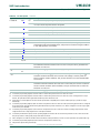
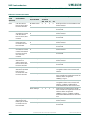
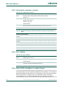
Document information
Info Content
Keywords LPC2141, LPC2142, LPC2144, LPC2146, LPC2148, LPC2000, LPC214x,
ARM, ARM7, embedded, 32-bit, microcontroller, USB 2.0, USB device
Abstract LPC214x User Manual

UM10139 All information provided in this document is subject to legal disclaimers. © NXP B.V. 2012. All rights reserved.
User manual Rev. 4 — 23 April 2012 2 of 354
Contact information
For more information, please visit: http://www.nxp.com
For sales office addresses, please send an email to: [email protected]
NXP Semiconductors
UM10139
LPC2141/2/4/6/8
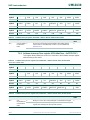
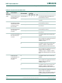
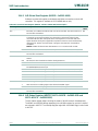
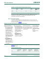
Revision history
Rev Date Description
4 20120423 Modifications:
• Device revision register added (see Section 21.8.11).
• Bit PCUSB in the PCONP register must be set to one to access the USB SRAM (see
Table 31
).
3 20101004 Modifications:
• New document template applied.
• I2C chapter: multiple errors corrected (Chapter 14 “LPC214x I2C-bus interface
I2C0/1”).
• IAP call example updated (Section 21.9).
• WDFEED register description updated Section 16.4.3 “Watchdog Feed register
(WDFEED - 0xE000 0008)”.
• RTC usage note updated (Section 18.5 “RTC usage notes”).
• CTCR register bit description corrected (Section 18.4.4 “Clock Tick Counter Register
(CTCR - 0xE002 4004)”).
• PINSEL2 register description updated (Section 6.4.3 “Pin function Select register 2
(PINSEL2 - 0xE002 C014)”).
• PWM TCR register bit 3 description updated (Section 16.4.2 “PWM Timer Control
Register (PWMTCR - 0xE001 4004)”).
• U0IER register bit description corrected (Section 10.3.6 “UART0 Interrupt Enable
Register (U0IER - 0xE000 C004, when DLAB = 0)”).
• U1IER register bit description corrected (Section 11.3.6 “UART1 Interrupt Enable
Register (U1IER - 0xE001 0004, when DLAB = 0)”).
• Pin description updated for VBAT, VREF, and RTCX1/2 (Section 5.2 “Pin description for
LPC2141/2/4/6/8”).
• SSP CR0 register corrected (Section 13.4.1 “SSP Control Register 0 (SSPCR0 -
0xE006 8000)”).
• ADC maximum voltage updated (Table 278 “ADC pin description”).
• Minimum DLL value for use with fractional divider corrected (Section 10.3.4 “UART0
Fractional Divider Register (U0FDR - 0xE000 C028)” and Section 11.3.4 “UART1
Fractional Divider Register (U1FDR - 0xE001 0028)”).
• CRP levels updated (Section 21.7 “Code Read Protection (CRP)”).
• Numerous editorial updates throughout the user manual.
2 20061030 LPC2141/2/4/6/8 user manual
1 20050815 Initial version

UM10139 All information provided in this document is subject to legal disclaimers. © NXP B.V. 2012. All rights reserved.
User manual Rev. 4 — 23 April 2012 3 of 354
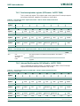
1.1 Introduction
The LPC2141/2/4/6/8 microcontrollers are based on a 32/16 bit ARM7TDMI-S CPU with
real-time emulation and embedded trace support, that combines the microcontroller with
embedded high speed flash memory ranging from 32 kB to 512 kB. A 128-bit wide
memory interface and a unique accelerator architecture enable 32-bit code execution at
the maximum clock rate. For critical code size applications, the alternative 16-bit Thumb
mode reduces code by more than 30 % with minimal performance penalty.
Due to their tiny size and low power consumption, LPC2141/2/4/6/8 are ideal for
applications where miniaturization is a key requirement, such as access control and
point-of-sale. A blend of serial communications interfaces ranging from a USB 2.0 Full
Speed device, multiple UARTs, SPI, SSP to I
2
Cs, and on-chip SRAM of 8 kB up to 40 kB,
make these devices very well suited for communication gateways and protocol
converters, soft modems, voice recognition and low end imaging, providing both large
buffer size and high processing power. Various 32-bit timers, single or dual 10-bit ADC(s),
10-bit DAC, PWM channels and 45 fast GPIO lines with up to nine edge or level sensitive
external interrupt pins make these microcontrollers particularly suitable for industrial
control and medical systems.
1.2 Features
• 16/32-bit ARM7TDMI-S microcontroller in a tiny LQFP64 package.
• 8 to 40 kB of on-chip static RAM and 32 to 512 kB of on-chip flash program memory.
128 bit wide interface/accelerator enables high speed 60 MHz operation.
• In-System/In-Application Programming (ISP/IAP) via on-chip boot-loader software.
Single flash sector or full chip erase in 400 ms and programming of 256 bytes in 1 ms.
• EmbeddedICE RT and Embedded Trace interfaces offer real-time debugging with the
on-chip RealMonitor software and high speed tracing of instruction execution.
• USB 2.0 Full Speed compliant Device Controller with 2 kB of endpoint RAM.
In addition, the LPC2146/8 provide 8 kB of on-chip RAM accessible to USB by DMA.
• One or two (LPC2141/2 vs. LPC2144/6/8) 10-bit A/D converters provide a total of 6/14
analog inputs, with conversion times as low as 2.44 s per channel.
• Single 10-bit D/A converter provides variable analog output.
• Two 32-bit timers/external event counters (with four capture and four compare
channels each), PWM unit (six outputs) and watchdog.
• Low power real-time clock with independent power and dedicated 32 kHz clock input.
• Multiple serial interfaces including two UARTs (16C550), two Fast I
2
C-bus
(400 kbit/s), SPI and SSP with buffering and variable data length capabilities.
• Vectored interrupt controller with configurable priorities and vector addresses.
• Up to 45 of 5 V tolerant fast general purpose I/O pins in a tiny LQFP64 package.
• Up to nine edge or level sensitive external interrupt pins available.
UM10139
Chapter 1: Introductory information
Rev. 4 — 23 April 2012 User manual

UM10139 All information provided in this document is subject to legal disclaimers. © NXP B.V. 2012. All rights reserved.
User manual Rev. 4 — 23 April 2012 4 of 354
NXP Semiconductors
UM10139
Chapter 1: Introductory information
• 60 MHz maximum CPU clock available from programmable on-chip PLL with settling
time of 100 s.
• On-chip integrated oscillator operates with an external crystal in range from 1 MHz to
30 MHz and with an external oscillator up to 50 MHz.
• Power saving modes include Idle and Power-down.
• Individual enable/disable of peripheral functions as well as peripheral clock scaling for
additional power optimization.
• Processor wake-up from Power-down mode via external interrupt, USB, Brown-Out
Detect (BOD) or Real-Time Clock (RTC).
• Single power supply chip with Power-On Reset (POR) and BOD circuits:
– CPU operating voltage range of 3.0 V to 3.6 V (3.3 V 10 %) with 5 V tolerant I/O
pads.
1.3 Applications
• Industrial control
• Medical systems
• Access control
• Point-of-sale
• Communication gateway
• Embedded soft modem
• General purpose applications
1.4 Device information
[1] While the USB DMA is the primary user of the additional 8 kB RAM, this RAM is also accessible at any time by the CPU as a general
purpose RAM for data and code storage.
1.5 Architectural overview
The LPC2141/2/4/6/8 consists of an ARM7TDMI-S CPU with emulation support, the
ARM7 Local Bus for interface to on-chip memory controllers, the AMBA Advanced
High-performance Bus (AHB) for interface to the interrupt controller, and the ARM
Table 1. LPC2141/2/4/6/8 device information
Device Number
of pins
On-chip
SRAM
Endpoint
USB RAM
On-chip
FLASH
Number of
10-bit ADC
channels
Number of
10-bit DAC
channels
Note
LPC2141 64 8kB 2kB 32kB 6 - -
LPC2142 64 16 kB 2 kB 64 kB 6 1 -
LPC2144 64 16 kB 2 kB 128 kB 14 1 UART1 with full
modem interface
LPC2146 64 32 kB + 8 kB
[1]
2 kB 256 kB 14 1 UART1 with full
modem interface
LPC2148 64 32 kB + 8 kB
[1]
2 kB 512 kB 14 1 UART1 with full
modem interface

UM10139 All information provided in this document is subject to legal disclaimers. © NXP B.V. 2012. All rights reserved.
User manual Rev. 4 — 23 April 2012 5 of 354
NXP Semiconductors
UM10139
Chapter 1: Introductory information
Peripheral Bus (APB, a compatible superset of ARM’s AMBA Advanced Peripheral Bus)
for connection to on-chip peripheral functions. The LPC2141/24/6/8 configures the
ARM7TDMI-S processor in little-endian byte order.
AHB peripherals are allocated a 2 megabyte range of addresses at the very top of the
4 gigabyte ARM memory space. Each AHB peripheral is allocated a 16 kB address space
within the AHB address space. LPC2141/2/4/6/8 peripheral functions (other than the
interrupt controller) are connected to the APB bus. The AHB to APB bridge interfaces the
APB bus to the AHB bus. APB peripherals are also allocated a 2 megabyte range of
addresses, beginning at the 3.5 gigabyte address point. Each APB peripheral is allocated
a 16 kB address space within the APB address space.
The connection of on-chip peripherals to device pins is controlled by a Pin Connect Block
(see chapter "Pin Connect Block" on page 58). This must be configured by software to fit
specific application requirements for the use of peripheral functions and pins.
1.6 ARM7TDMI-S processor
The ARM7TDMI-S is a general purpose 32-bit microprocessor, which offers high
performance and very low power consumption. The ARM architecture is based on
Reduced Instruction Set Computer (RISC) principles, and the instruction set and related
decode mechanism are much simpler than those of microprogrammed Complex
Instruction Set Computers. This simplicity results in a high instruction throughput and
impressive real-time interrupt response from a small and cost-effective processor core.
Pipeline techniques are employed so that all parts of the processing and memory systems
can operate continuously. Typically, while one instruction is being executed, its successor
is being decoded, and a third instruction is being fetched from memory.
The ARM7TDMI-S processor also employs a unique architectural strategy known as
THUMB, which makes it ideally suited to high-volume applications with memory
restrictions, or applications where code density is an issue.
The key idea behind THUMB is that of a super-reduced instruction set. Essentially, the
ARM7TDMI-S processor has two instruction sets:
• The standard 32-bit ARM instruction set.
• A 16-bit THUMB instruction set.
The THUMB set’s 16-bit instruction length allows it to approach twice the density of
standard ARM code while retaining most of the ARM’s performance advantage over a
traditional 16-bit processor using 16-bit registers. This is possible because THUMB code
operates on the same 32-bit register set as ARM code.
THUMB code is able to provide up to 65% of the code size of ARM, and 160% of the
performance of an equivalent ARM processor connected to a 16-bit memory system.
The ARM7TDMI-S processor is described in detail in the ARM7TDMI-S Datasheet that
can be found on official ARM website.

UM10139 All information provided in this document is subject to legal disclaimers. © NXP B.V. 2012. All rights reserved.
User manual Rev. 4 — 23 April 2012 6 of 354
NXP Semiconductors
UM10139
Chapter 1: Introductory information
1.7 On-chip flash memory system
The LPC2141/2/4/6/8 incorporate a 32 kB, 64 kB, 128 kB, 256 kB, and 512 kB Flash
memory system, respectively. This memory may be used for both code and data storage.
Programming of the Flash memory may be accomplished in several ways: over the serial
built-in JTAG interface, using In System Programming (ISP) and UART0, or by means of
In Application Programming (IAP) capabilities. The application program, using the IAP
functions, may also erase and/or program the Flash while the application is running,
allowing a great degree of flexibility for data storage field firmware upgrades, etc. When
the LPC2141/2/4/6/8 on-chip bootloader is used, 32 kB, 64 kB, 128 kB, 256 kB, and
500 kB of Flash memory is available for user code.
The LPC2141/2/4/6/8 Flash memory provides minimum of 100,000 erase/write cycles and
20 years of data-retention.
1.8 On-chip Static RAM (SRAM)
On-chip Static RAM (SRAM) may be used for code and/or data storage. The on-chip
SRAM may be accessed as 8-bits, 16-bits, and 32-bits. The LPC2141/2/4/6/8 provide
8/16/32 kB of static RAM, respectively.
The LPC2141/2/4/6/8 SRAM is designed to be accessed as a byte-addressed memory.
Word and halfword accesses to the memory ignore the alignment of the address and
access the naturally-aligned value that is addressed (so a memory access ignores
address bits 0 and 1 for word accesses, and ignores bit 0 for halfword accesses).
Therefore valid reads and writes require data accessed as halfwords to originate from
addresses with address line 0 being 0 (addresses ending with 0, 2, 4, 6, 8, A, C, and E in
hexadecimal notation) and data accessed as words to originate from addresses with
address lines 0 and 1 being 0 (addresses ending with 0, 4, 8, and C in hexadecimal
notation). This rule applies to both off and on-chip memory usage.
The SRAM controller incorporates a write-back buffer in order to prevent CPU stalls
during back-to-back writes. The write-back buffer always holds the last data sent by
software to the SRAM. This data is only written to the SRAM when another write is
requested by software (the data is only written to the SRAM when software does another
write). If a chip reset occurs, actual SRAM contents will not reflect the most recent write
request (i.e. after a "warm" chip reset, the SRAM does not reflect the last write operation).
Any software that checks SRAM contents after reset must take this into account. Two
identical writes to a location guarantee that the data will be present after a Reset.
Alternatively, a dummy write operation before entering idle or power-down mode will
similarly guarantee that the last data written will be present in SRAM after a subsequent
Reset.

UM10139 All information provided in this document is subject to legal disclaimers. © NXP B.V. 2012. All rights reserved.
User manual Rev. 4 — 23 April 2012 7 of 354
NXP Semiconductors
UM10139
Chapter 1: Introductory information
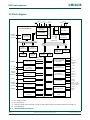
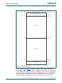
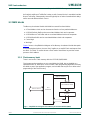
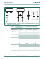
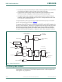
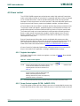
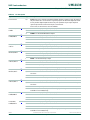
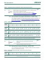
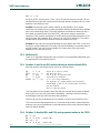
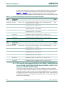
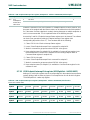
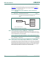
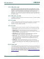
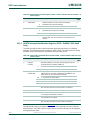
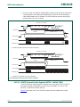
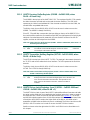
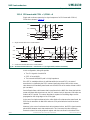
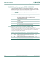
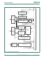
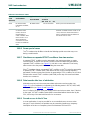
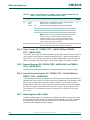
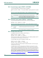
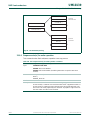
1.9 Block diagram
(1) Pins shared with GPIO.
(2) LPCC2144/6/8 only.
(3) USB DMA controller with 8 kB of RAM accessible as general purpose RAM and/or DMA is available in LPC2146/8 only.
(4) LPC2142/4/6/8 only.
Fig 1. LPC2141/2/4/6/8 block diagram
SCL0,1
P0[31:28],
P0[25:0]
P1[31:16]
P0[31:28],
P0[25:0]
P1[31:16]
SDA0,1
XTAL2
XTAL1
SCK0,1
MOSI0,1
MISO0,1
EINT[3:0]
AD0[7:6],
AD0[4:0]
PWM[6:1]
SSEL0,1
TXD0,1
RXD0,1
AHB BRIDGE
PLL0
PLL1
UART0/UART1
REAL TIME CLOCK
PWM0
ARM7TDMI-S
RESET
LPC2141/42/44/46/48
8 CAP
8 MAT
AD1[7:0]
(2)
AOUT
(4)
DSR1
(2)
,CTS1
(2)
RTS1
(2)
, DTR1
(2)
DCD1
(2)
, RI1
(2)
002aab560
TRST
(1)
TMS
(1)
TCK
(1)
TDI
(1)
TDO
(1)
trace
signals
FAST GENERAL
PURPOSE I/O
INTERNAL
SRAM
CONTROLLER
INTERNAL
FLASH
CONTROLLER
8/16/32 kB
SRAM
32/64/128/
256/512 kB
FLASH
EXTERNAL
INTERRUPTS
CAPTURE/
COMPARE
TIMER 0/TIMER 1
A/D CONVERTERS
0 AND 1
(2)
D/A CONVERTER
(4)
GENERAL
PURPOSE I/O
SYSTEM
CONTROL
WATCHDOG
TIMER
RTCX2
RTCX1
SPI AND SSP
SERIAL INTERFACES
I
2
C SERIAL
INTERFACES 0 AND 1
APB (ARM
peripheral bus)
AHB TO APB
BRIDGE
APB
DIVIDER
AHB
DECODER
AMBA AHB
(Advanced High-performance Bus)
VECTORED
INTERRUPT
CONTROLLER
SYSTEM
FUNCTIONS
system
clock
EMULATION
TRACE MODULE
TEST/DEBUG
INTERFACE
ARM7 local bus
V
BAT
8 kB RAM
SHARED WITH
USB DMA
(3)
D+
D-
UP_LED
CONNECT
V
BUS
USB 2.0 FULL-SPEED
DEVICE CONTROLLER
WITH DMA
(3)
USB
clock

UM10139 All information provided in this document is subject to legal disclaimers. © NXP B.V. 2012. All rights reserved.
User manual Rev. 4 — 23 April 2012 8 of 354
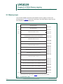
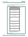
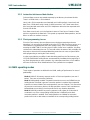
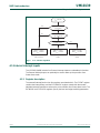
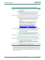
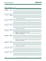
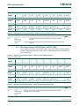
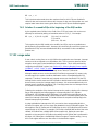
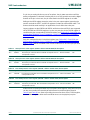
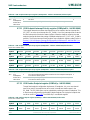
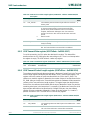
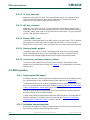
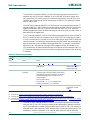
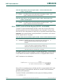
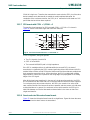
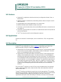
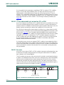
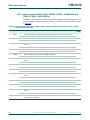
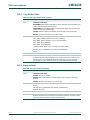
2.1 Memory maps
The LPC2141/2/4/6/8 incorporates several distinct memory regions, shown in the
following figures. Figure 2
shows the overall map of the entire address space from the
user program viewpoint following reset.
UM10139
Chapter 2: LPC214x Memory mapping
Rev. 4 — 23 April 2012 User manual
Set bit PUSB in the PCONP register (Table 31) to access the 8 kB USB SRAM.
Fig 2. System memory map
TOTAL OF 32 kB ON-CHIP NON-VOLATILE MEMORY (LPC2141)
0xC000 0000
0x8000 0000
0x0000 0000
0.0 GB
1.0 GB
2.0 GB
3.75 GB
4.0 GB
3.0 GB
TOTAL OF 64 kB ON-CHIP NON-VOLATILE MEMORY (LPC2142)
RESERVED ADDRESS SPACE
8 kB ON-CHIP STATIC RAM (LPC2141)
16 kB ON-CHIP STATIC RAM (LPC2142/2144)
32 kB ON-CHIP STATIC RAM (LPC2146/2148)
RESERVED ADDRESS SPACE
BOOT BLOCK
(12 kB REMAPPED FROM ON-CHIP FLASH MEMORY)
RESERVED ADDRESS SPACE
AHB PERIPHERALS
APB PERIPHERALS
3.5 GB
0x4000 4000
0x4000 3FFF
0x4000 8000
0x4000 7FFF
0xE000 0000
0xF000 0000
0xFFFF FFFF
TOTAL OF 128 kB ON-CHIP NON-VOLATILE MEMORY (LPC2144)
TOTAL OF 256 kB ON-CHIP NON-VOLATILE MEMORY (LPC2146)
TOTAL OF 512 kB ON-CHIP NON-VOLATILE MEMORY (LPC2148)
0x4000 2000
0x4000 1FFF
0x0000 8000
0x0000 7FFF
0x0001 0000
0x0000 FFFF
0x0002 0000
0x0001 FFFF
0x0004 0000
0x0003 FFFF
0x0008 0000
0x0007 FFFF
8 kB ON-CHIP USB DMA RAM (LPC2146/2148)
0x7FD0 0000
0x7FCF FFFF
0x7FD0 2000
0x7FD0 1FFF
RESERVED ADDRESS SPACE
0x7FFF D000
0x7FFF CFFF
0x4000 0000
0x3FFF FFFF

UM10139 All information provided in this document is subject to legal disclaimers. © NXP B.V. 2012. All rights reserved.
User manual Rev. 4 — 23 April 2012 9 of 354
NXP Semiconductors
UM10139
Chapter 2: LPC214x Memory mapping
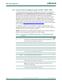
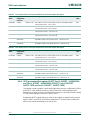
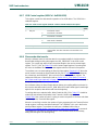
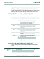
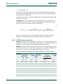
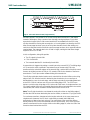
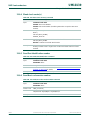
Figures 3 through 4 and Table 2 show different views of the peripheral address space.
Both the AHB and APB peripheral areas are 2 megabyte spaces which are divided up into
128 peripherals. Each peripheral space is 16 kilobytes in size. This allows simplifying the
address decoding for each peripheral. All peripheral register addresses are word aligned
(to 32-bit boundaries) regardless of their size. This eliminates the need for byte lane
mapping hardware that would be required to allow byte (8-bit) or half-word (16-bit)
Fig 3. Peripheral memory map
RESERVED
RESERVED
0xF000 0000
0xEFFF FFFF
APB PERIPHERALS
0xE020 0000
0xE01F FFFF
0xE000 0000
AHB PERIPHERALS
0xFFFF FFFF
0xFFE0 0000
0xFFDF FFFF
3.75 GB
3.5 GB
3.5 GB + 2 MB
4.0 GB - 2 MB
4.0 GB

UM10139 All information provided in this document is subject to legal disclaimers. © NXP B.V. 2012. All rights reserved.
User manual Rev. 4 — 23 April 2012 10 of 354
NXP Semiconductors
UM10139
Chapter 2: LPC214x Memory mapping
accesses to occur at smaller boundaries. An implication of this is that word and half-word
registers must be accessed all at once. For example, it is not possible to read or write the
upper byte of a word register separately.
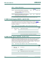
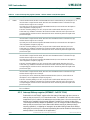
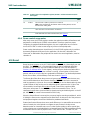
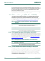
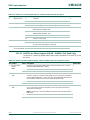
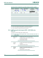
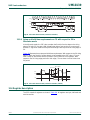
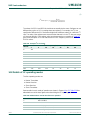
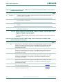
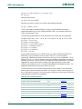
AHB section is 128 x 16 kB blocks (totaling 2 MB).
APB section is 128 x 16 kB blocks (totaling 2MB).
Fig 4. AHB peripheral map
VECTORED INTERRUPT CONTROLLER
(AHB PERIPHERAL #0)
0xFFFF F000 (4G - 4K)
0xFFFF C000
0xFFFF 8000
(AHB PERIPHERAL #125)
(AHB PERIPHERAL #124)
(AHB PERIPHERAL #3)
(AHB PERIPHERAL #2)
(AHB PERIPHERAL #1)
(AHB PERIPHERAL #126)
0xFFFF 4000
0xFFFF 0000
0xFFE1 0000
0xFFE0 C000
0xFFE0 8000
0xFFE0 4000
0xFFE0 0000

UM10139 All information provided in this document is subject to legal disclaimers. © NXP B.V. 2012. All rights reserved.
User manual Rev. 4 — 23 April 2012 11 of 354
NXP Semiconductors
UM10139
Chapter 2: LPC214x Memory mapping
2.2 LPC2141/2142/2144/2146/2148 memory re-mapping and boot block
2.2.1 Memory map concepts and operating modes
The basic concept on the LPC2141/2/4/6/8 is that each memory area has a "natural"
location in the memory map. This is the address range for which code residing in that area
is written. The bulk of each memory space remains permanently fixed in the same
location, eliminating the need to have portions of the code designed to run in different
address ranges.
Because of the location of the interrupt vectors on the ARM7 processor (at addresses
0x0000 0000 through 0x0000 001C, as shown in Table 3
below), a small portion of the
Boot Block and SRAM spaces need to be re-mapped in order to allow alternative uses of
interrupts in the different operating modes described in Table 4
. Re-mapping of the
interrupts is accomplished via the Memory Mapping Control feature (Section 4.7 “
Memory
mapping control” on page 32).
Table 2. APB peripherals and base addresses
APB peripheral Base address Peripheral name
0 0xE000 0000 Watchdog timer
1 0xE000 4000 Timer 0
2 0xE000 8000 Timer 1
3 0xE000 C000 UART0
4 0xE001 0000 UART1
5 0xE001 4000 PWM
6 0xE001 8000 Not used
7 0xE001 C000 I
2
C0
8 0xE002 0000 SPI0
9 0xE002 4000 RTC
10 0xE002 8000 GPIO
11 0xE002 C000 Pin connect block
12 0xE003 0000 Not used
13 0xE003 4000 ADC0
14 - 22 0xE003 8000
0xE005 8000
Not used
23 0xE005 C000 I
2
C1
24 0xE006 0000 ADC1
25 0xE006 4000 Not used
26 0xE006 8000 SSP
27 0xE006 C000 DAC
28 - 35 0xE007 0000
0xE008 C000
Not used
36 0xE009 0000 USB
37 - 126 0xE009 4000
0xE01F 8000
Not used
127 0xE01F C000 System Control Block

UM10139 All information provided in this document is subject to legal disclaimers. © NXP B.V. 2012. All rights reserved.
User manual Rev. 4 — 23 April 2012 12 of 354
NXP Semiconductors
UM10139
Chapter 2: LPC214x Memory mapping
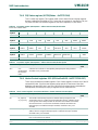
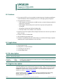
2.2.2 Memory re-mapping
In order to allow for compatibility with future derivatives, the entire Boot Block is mapped
to the top of the on-chip memory space. In this manner, the use of larger or smaller flash
modules will not require changing the location of the Boot Block (which would require
changing the Boot Loader code itself) or changing the mapping of the Boot Block interrupt
vectors. Memory spaces other than the interrupt vectors remain in fixed locations.
Figure 5
shows the on-chip memory mapping in the modes defined above.
The portion of memory that is re-mapped to allow interrupt processing in different modes
includes the interrupt vector area (32 bytes) and an additional 32 bytes, for a total of
64 bytes. The re-mapped code locations overlay addresses 0x0000 0000 through
0x0000 003F. A typical user program in the Flash memory can place the entire FIQ
handler at address 0x0000 001C without any need to consider memory boundaries. The
vector contained in the SRAM, external memory, and Boot Block must contain branches to
the actual interrupt handlers, or to other instructions that accomplish the branch to the
interrupt handlers.
There are three reasons this configuration was chosen:
1. To give the FIQ handler in the Flash memory the advantage of not having to take a
memory boundary caused by the remapping into account.
Table 3. ARM exception vector locations
Address Exception
0x0000 0000 Reset
0x0000 0004 Undefined Instruction
0x0000 0008 Software Interrupt
0x0000 000C Prefetch Abort (instruction fetch memory fault)
0x0000 0010 Data Abort (data access memory fault)
0x0000 0014 Reserved
Note: Identified as reserved in ARM documentation, this location is used
by the Boot Loader as the Valid User Program key. This is described in
detail in "Flash Memory System and Programming" chapter on page 296.
0x0000 0018 IRQ
0x0000 001C FIQ
Table 4. LPC2141/2/4/6/8 memory mapping modes
Mode Activation Usage
Boot
Loader
mode
Hardware
activation by
any Reset
The Boot Loader always executes after any reset. The Boot Block
interrupt vectors are mapped to the bottom of memory to allow
handling exceptions and using interrupts during the Boot Loading
process.
User
Flash
mode
Software
activation by
Boot code
Activated by Boot Loader when a valid User Program Signature is
recognized in memory and Boot Loader operation is not forced.
Interrupt vectors are not re-mapped and are found in the bottom of the
Flash memory.
User RAM
mode
Software
activation by
User program
Activated by a User Program as desired. Interrupt vectors are
re-mapped to the bottom of the Static RAM.

UM10139 All information provided in this document is subject to legal disclaimers. © NXP B.V. 2012. All rights reserved.
User manual Rev. 4 — 23 April 2012 13 of 354
NXP Semiconductors
UM10139
Chapter 2: LPC214x Memory mapping
2. Minimize the need to for the SRAM and Boot Block vectors to deal with arbitrary
boundaries in the middle of code space.
3. To provide space to store constants for jumping beyond the range of single word
branch instructions.
Re-mapped memory areas, including the Boot Block and interrupt vectors, continue to
appear in their original location in addition to the re-mapped address.
Details on re-mapping and examples can be found in Section 4.7 “
Memory mapping
control” on page 32.

UM10139 All information provided in this document is subject to legal disclaimers. © NXP B.V. 2012. All rights reserved.
User manual Rev. 4 — 23 April 2012 14 of 354
NXP Semiconductors
UM10139
Chapter 2: LPC214x Memory mapping
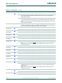
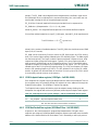
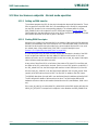
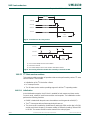
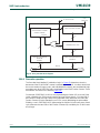
Remark: Memory regions are not drawn to scale.
Fig 5. Map of lower memory is showing re-mapped and re-mappable areas (LPC2148
with 512 kB Flash)
12 kB BOOT BLOCK
(RE-MAPPED FROM TOP OF FLASH MEMORY)
RESERVED ADDRESSING SPACE
32 kB ON-CHIP SRAM
0.0 GB
ACTIVE INTERRUPT VECTORS (FROM FLASH, SRAM, OR BOOT
BLOCK)
0x8000 0000
0x4000 8000
0x4000 7FFF
0x4000 0000
0x3FFF FFFF
0x0000 0000
0x7FFF FFFF
1.0 GB
2.0 GB - 12 kB
2.0 GB
(BOOT BLOCK INTERRUPT VECTORS)
(SRAM INTERRUPT VECTORS)
512 kB FLASH MEMORY
(12 kB BOOT BLOCK RE-MAPPED TO HIGHER ADDRESS RANGE)
0x0008 0000
0x0007 FFFF
RESERVED ADDRESSING SPACE
0x7FFF D000
0x7FFF CFFF

UM10139 All information provided in this document is subject to legal disclaimers. © NXP B.V. 2012. All rights reserved.
User manual Rev. 4 — 23 April 2012 15 of 354
NXP Semiconductors
UM10139
Chapter 2: LPC214x Memory mapping
2.3 Prefetch abort and data abort exceptions
The LPC2141/2/4/6/8 generates the appropriate bus cycle abort exception if an access is
attempted for an address that is in a reserved or unassigned address region. The regions
are:
• Areas of the memory map that are not implemented for a specific ARM derivative. For
the LPC2141/2/4/6/8, this is:
– Address space between On-Chip Non-Volatile Memory and On-Chip SRAM,
labelled "Reserved Address Space" in Figure 2
. For 32 kB Flash device this is
memory address range from 0x0000 8000 to 0x3FFF FFFF, for 64 kB Flash device
this is memory address range from 0x0001 0000 to 0x3FFF FFFF, for 128 kB
Flash device this is memory address range from 0x0002 0000 to 0x3FFF FFFF, for
256 kB Flash device this is memory address range from 0x0004 0000 to
0x3FFF FFFF while for 512 kB Flash device this range is from 0x0008 0000 to
0x3FFF FFFF.
– Address space between On-Chip Static RAM and the Boot Block. Labelled
"Reserved Address Space" in Figure 2
. For 8 kB SRAM device this is memory
address range from 0x4000 2000 to 0x7FFF CFFF, for 16 kB SRAM device this is
memory address range from 0x4000 4000 to 0x7FFF CFFF. For 32 kB SRAM
device this range is from 0x4000 8000 to 0x7FCF FFFF where the 8 kB USB DMA
RAM starts, and from 0x7FD0 2000 to 0x7FFF CFFF.
– Address space between 0x8000 0000 and 0xDFFF FFFF, labelled "Reserved
Adress Space".
– Reserved regions of the AHB and APB spaces. See Figure 3
.
• Unassigned AHB peripheral spaces. See Figure 4.
• Unassigned APB peripheral spaces. See Table 2.
For these areas, both attempted data access and instruction fetch generate an exception.
In addition, a Prefetch Abort exception is generated for any instruction fetch that maps to
an AHB or APB peripheral address.
Within the address space of an existing APB peripheral, a data abort exception is not
generated in response to an access to an undefined address. Address decoding within
each peripheral is limited to that needed to distinguish defined registers within the
peripheral itself. For example, an access to address 0xE000 D000 (an undefined address
within the UART0 space) may result in an access to the register defined at address
0xE000 C000. Details of such address aliasing within a peripheral space are not defined
in the LPC2141/2/4/6/8 documentation and are not a supported feature.
Note that the ARM core stores the Prefetch Abort flag along with the associated
instruction (which will be meaningless) in the pipeline and processes the abort only if an
attempt is made to execute the instruction fetched from the illegal address. This prevents
accidental aborts that could be caused by prefetches that occur when code is executed
very near a memory boundary.

UM10139 All information provided in this document is subject to legal disclaimers. © NXP B.V. 2012. All rights reserved.
User manual Rev. 4 — 23 April 2012 16 of 354
3.1 Introduction
The MAM block in the LPC2141/2/4/6/8 maximizes the performance of the ARM
processor when it is running code in Flash memory, but does so using a single Flash
bank.
3.2 Operation
Simply put, the Memory Accelerator Module (MAM) attempts to have the next ARM
instruction that will be needed in its latches in time to prevent CPU fetch stalls. The
LPC2141/2/4/6/8 uses one bank of Flash memory, compared to the two banks used on
predecessor devices. It includes three 128-bit buffers called the Prefetch Buffer, the
Branch Trail Buffer and the data buffer. When an Instruction Fetch is not satisfied by either
the Prefetch or Branch Trail Buffer, nor has a prefetch been initiated for that line, the ARM
is stalled while a fetch is initiated for the 128-bit line. If a prefetch has been initiated but not
yet completed, the ARM is stalled for a shorter time. Unless aborted by a data access, a
prefetch is initiated as soon as the Flash has completed the previous access. The
prefetched line is latched by the Flash module, but the MAM does not capture the line in
its prefetch buffer until the ARM core presents the address from which the prefetch has
been made. If the core presents a different address from the one from which the prefetch
has been made, the prefetched line is discarded.
The Prefetch and Branch Trail buffers each include four 32-bit ARM instructions or eight
16-bit Thumb instructions. During sequential code execution, typically the Prefetch Buffer
contains the current instruction and the entire Flash line that contains it.
The MAM differentiates between instruction and data accesses. Code and data accesses
use separate 128-bit buffers. 3 of every 4 sequential 32-bit code or data accesses "hit" in
the buffer without requiring a Flash access (7 of 8 sequential 16-bit accesses, 15 of every
16 sequential byte accesses). The fourth (eighth, 16th) sequential data access must
access Flash, aborting any prefetch in progress. When a Flash data access is concluded,
any prefetch that had been in progress is re-initiated.
Timing of Flash read operations is programmable and is described later in this section.
In this manner, there is no code fetch penalty for sequential instruction execution when the
CPU clock period is greater than or equal to one fourth of the Flash access time. The
average amount of time spent doing program branches is relatively small (less than 25%)
and may be minimized in ARM (rather than Thumb) code through the use of the
conditional execution feature present in all ARM instructions. This conditional execution
may often be used to avoid small forward branches that would otherwise be necessary.
Branches and other program flow changes cause a break in the sequential flow of
instruction fetches described above. The Branch Trail Buffer captures the line to which
such a non-sequential break occurs. If the same branch is taken again, the next
instruction is taken from the Branch Trail Buffer. When a branch outside the contents of
UM10139
Chapter 3: LPC214x Memory accelerator module
Rev. 4 — 23 April 2012 User manual

UM10139 All information provided in this document is subject to legal disclaimers. © NXP B.V. 2012. All rights reserved.
User manual Rev. 4 — 23 April 2012 17 of 354
NXP Semiconductors
UM10139
Chapter 3: LPC214x Memory accelerator module
the Prefetch and Branch Trail Buffer is taken, a stall of several clocks is needed to load the
Branch Trail buffer. Subsequently, there will typically be no further instructionfetch delays
until a new and different branch occurs.
3.3 MAM blocks
The Memory Accelerator Module is divided into several functional blocks:
• A Flash Address Latch and an incrementor function to form prefetch addresses
• A 128-bit Prefetch Buffer and an associated Address latch and comparator
• A 128-bit Branch Trail Buffer and an associated Address latch and comparator
• A 128-bit Data Buffer and an associated Address latch and comparator
• Control logic
• Wait logic
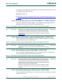
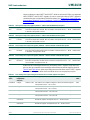
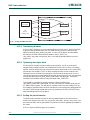
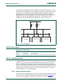
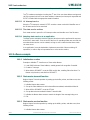
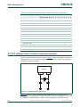
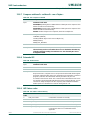
Figure 6
shows a simplified block diagram of the Memory Accelerator Module data paths.
In the following descriptions, the term “fetch” applies to an explicit Flash read request from
the ARM. “Pre-fetch” is used to denote a Flash read of instructions beyond the current
processor fetch address.
3.3.1 Flash memory bank
There is one bank of Flash memory with the LPC2141/2/4/6/8 MAM.
Flash programming operations are not controlled by the MAM, but are handled as a
separate function. A “boot block” sector contains Flash programming algorithms that may
be called as part of the application program, and a loader that may be run to allow serial
programming of the Flash memory.
Fig 6. Simplified block diagram of the Memory Accelerator Module (MAM)
BUS
INTERFACE
BUFFERS
MEMORY ADDRESS
ARM LOCAL BUS
FLASH MEMORY BANK

UM10139 All information provided in this document is subject to legal disclaimers. © NXP B.V. 2012. All rights reserved.
User manual Rev. 4 — 23 April 2012 18 of 354
NXP Semiconductors
UM10139
Chapter 3: LPC214x Memory accelerator module
3.3.2 Instruction latches and data latches
Code and Data accesses are treated separately by the Memory Accelerator Module.
There is a 128-bit Latch, a 15-bit Address
Latch, and a 15-bit comparator associated with each buffer (prefetch, branch trail, and
data). Each 128-bit latch holds 4 words (4 ARM instructions, or 8 Thumb instructions).
Also associated with each buffer are 32 4:1 Multiplexers that select the requested word
from the 128-bit line.
Each Data access that is not in the Data latch causes a Flash fetch of 4 words of data,
which are captured in the Data latch. This speeds up sequential Data operations, but has
little or no effect on random accesses.
3.3.3 Flash programming issues
Since the Flash memory does not allow accesses during programming and erase
operations, it is necessary for the MAM to force the CPU to wait if a memory access to a
Flash address is requested while the Flash module is busy. (This is accomplished by
asserting the ARM7TDMI-S local bus signal CLKEN.) Under some conditions, this delay
could result in a Watchdog time-out. The user will need to be aware of this possibility and
take steps to insure that an unwanted Watchdog reset does not cause a system failure
while programming or erasing the Flash memory.
In order to preclude the possibility of stale data being read from the Flash memory, the
LPC2141/2/4/6/8 MAM holding latches are automatically invalidated at the beginning of
any Flash programming or erase operation. Any subsequent read from a Flash address
will cause a new fetch to be initiated after the Flash operation has completed.
3.4 MAM operating modes
Three modes of operation are defined for the MAM, trading off performance for ease of
predictability:
Mode 0: MAM off. All memory requests result in a Flash read operation (see note 2
below). There are no instruction prefetches.
Mode 1: MAM partially enabled. Sequential instruction accesses are fulfilled from the
holding latches if the data is present. Instruction prefetch is enabled. Non-sequential
instruction accesses initiate Flash read operations (see note 2 below). This means that
all branches cause memory fetches. All data operations cause a Flash read because
buffered data access timing is hard to predict and is very situation dependent.
Mode 2: MAM fully enabled. Any memory request (code or data) for a value that is
contained in one of the corresponding holding latches is fulfilled from the latch.
Instruction prefetch is enabled. Flash read operations are initiated for instruction
prefetch and code or data values not available in the corresponding holding latches.

UM10139 All information provided in this document is subject to legal disclaimers. © NXP B.V. 2012. All rights reserved.
User manual Rev. 4 — 23 April 2012 19 of 354
NXP Semiconductors
UM10139
Chapter 3: LPC214x Memory accelerator module
[1] Instruction prefetch is enabled in modes 1 and 2.
[2] The MAM actually uses latched data if it is available, but mimics the timing of a Flash read operation. This
saves power while resulting in the same execution timing. The MAM can truly be turned off by setting the
fetch timing value in MAMTIM to one clock.
[1] The MAM actually uses latched data if it is available, but mimics the timing of a Flash read operation. This
saves power while resulting in the same execution timing. The MAM can truly be turned off by setting the
fetch timing value in MAMTIM to one clock.
3.5 MAM configuration
After reset the MAM defaults to the disabled state. Software can turn memory access
acceleration on or off at any time. This allows most of an application to be run at the
highest possible performance, while certain functions can be run at a somewhat slower
but more predictable rate if more precise timing is required.
3.6 Register description
All registers, regardless of size, are on word address boundaries. Details of the registers
appear in the description of each function.
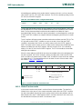
Table 5. MAM responses to program accesses of various types
Program Memory Request Type MAM Mode
0 1 2
Sequential access, data in latches Initiate Fetch
[2]
Use Latched
Data
[1]
Use Latched
Data
[1]
Sequential access, data not in latches Initiate Fetch Initiate Fetch
[1]
Initiate Fetch
[1]
Non-sequential access, data in latches Initiate Fetch
[2]
Initiate Fetch
[1][2]
Use Latched
Data
[1]
Non-sequential access, data not in latches Initiate Fetch Initiate Fetch
[1]
Initiate Fetch
[1]
Table 6. MAM responses to data and DMA accesses of various types
Data Memory Request Type MAM Mode
0 1 2
Sequential access, data in latches Initiate Fetch
[1]
Initiate Fetch
[1]
Use Latched
Data
Sequential access, data not in latches Initiate Fetch Initiate Fetch Initiate Fetch
Non-sequential access, data in latches Initiate Fetch
[1]
Initiate Fetch
[1]
Use Latched
Data
Non-sequential access, data not in latches Initiate Fetch Initiate Fetch Initiate Fetch

UM10139 All information provided in this document is subject to legal disclaimers. © NXP B.V. 2012. All rights reserved.
User manual Rev. 4 — 23 April 2012 20 of 354
NXP Semiconductors
UM10139
Chapter 3: LPC214x Memory accelerator module
[1] Reset value reflects the data stored in used bits only. It does not include reserved bits content.
3.7 MAM Control Register (MAMCR - 0xE01F C000)
Two configuration bits select the three MAM operating modes, as shown in Table 8.
Following Reset, MAM functions are disabled. Changing the MAM operating mode causes
the MAM to invalidate all of the holding latches, resulting in new reads of Flash
information as required.
3.8 MAM Timing register (MAMTIM - 0xE01F C004)
The MAM Timing register determines how many CCLK cycles are used to access the
Flash memory. This allows tuning MAM timing to match the processor operating
frequency. Flash access times from 1 clock to 7 clocks are possible. Single clock Flash
accesses would essentially remove the MAM from timing calculations. In this case the
MAM mode may be selected to optimize power usage.
Table 7. Summary of MAM registers
Name Description Access Reset
value
[1]
Address
MAMCR Memory Accelerator Module Control Register.
Determines the MAM functional mode, that is, to
what extent the MAM performance enhancements
are enabled. See Table 8
.
R/W 0x0 0xE01F C000
MAMTIM Memory Accelerator Module Timing control.
Determines the number of clocks used for Flash
memory fetches (1 to 7 processor clocks).
R/W 0x07 0xE01F C004
Table 8. MAM Control Register (MAMCR - address 0xE01F C000) bit description
Bit Symbol Value Description Reset
value
1:0 MAM_mode
_control
00 MAM functions disabled 0
01 MAM functions partially enabled
10 MAM functions fully enabled
11 Reserved. Not to be used in the application.
7:2 - - Reserved, user software should not write ones to reserved
bits. The value read from a reserved bit is not defined.
NA
Table 9. MAM Timing register (MAMTIM - address 0xE01F C004) bit description
Bit Symbol Value Description Reset
value
2:0 MAM_fetch_
cycle_timing
000 0 - Reserved. 07
001 1 - MAM fetch cycles are 1 processor clock (CCLK) in
duration
010 2 - MAM fetch cycles are 2 CCLKs in duration
011 3 - MAM fetch cycles are 3 CCLKs in duration
100 4 - MAM fetch cycles are 4 CCLKs in duration
101 5 - MAM fetch cycles are 5 CCLKs in duration
Page is loading ...
Page is loading ...
Page is loading ...
Page is loading ...
Page is loading ...
Page is loading ...
Page is loading ...
Page is loading ...
Page is loading ...
Page is loading ...
Page is loading ...
Page is loading ...
Page is loading ...
Page is loading ...
Page is loading ...
Page is loading ...
Page is loading ...
Page is loading ...
Page is loading ...
Page is loading ...
Page is loading ...
Page is loading ...
Page is loading ...
Page is loading ...
Page is loading ...
Page is loading ...
Page is loading ...
Page is loading ...
Page is loading ...
Page is loading ...
Page is loading ...
Page is loading ...
Page is loading ...
Page is loading ...
Page is loading ...
Page is loading ...
Page is loading ...
Page is loading ...
Page is loading ...
Page is loading ...
Page is loading ...
Page is loading ...
Page is loading ...
Page is loading ...
Page is loading ...
Page is loading ...
Page is loading ...
Page is loading ...
Page is loading ...
Page is loading ...
Page is loading ...
Page is loading ...
Page is loading ...
Page is loading ...
Page is loading ...
Page is loading ...
Page is loading ...
Page is loading ...
Page is loading ...
Page is loading ...
Page is loading ...
Page is loading ...
Page is loading ...
Page is loading ...
Page is loading ...
Page is loading ...
Page is loading ...
Page is loading ...
Page is loading ...
Page is loading ...
Page is loading ...
Page is loading ...
Page is loading ...
Page is loading ...
Page is loading ...
Page is loading ...
Page is loading ...
Page is loading ...
Page is loading ...
Page is loading ...
Page is loading ...
Page is loading ...
Page is loading ...
Page is loading ...
Page is loading ...
Page is loading ...
Page is loading ...
Page is loading ...
Page is loading ...
Page is loading ...
Page is loading ...
Page is loading ...
Page is loading ...
Page is loading ...
Page is loading ...
Page is loading ...
Page is loading ...
Page is loading ...
Page is loading ...
Page is loading ...
Page is loading ...
Page is loading ...
Page is loading ...
Page is loading ...
Page is loading ...
Page is loading ...
Page is loading ...
Page is loading ...
Page is loading ...
Page is loading ...
Page is loading ...
Page is loading ...
Page is loading ...
Page is loading ...
Page is loading ...
Page is loading ...
Page is loading ...
Page is loading ...
Page is loading ...
Page is loading ...
Page is loading ...
Page is loading ...
Page is loading ...
Page is loading ...
Page is loading ...
Page is loading ...
Page is loading ...
Page is loading ...
Page is loading ...
Page is loading ...
Page is loading ...
Page is loading ...
Page is loading ...
Page is loading ...
Page is loading ...
Page is loading ...
Page is loading ...
Page is loading ...
Page is loading ...
Page is loading ...
Page is loading ...
Page is loading ...
Page is loading ...
Page is loading ...
Page is loading ...
Page is loading ...
Page is loading ...
Page is loading ...
Page is loading ...
Page is loading ...
Page is loading ...
Page is loading ...
Page is loading ...
Page is loading ...
Page is loading ...
Page is loading ...
Page is loading ...
Page is loading ...
Page is loading ...
Page is loading ...
Page is loading ...
Page is loading ...
Page is loading ...
Page is loading ...
Page is loading ...
Page is loading ...
Page is loading ...
Page is loading ...
Page is loading ...
Page is loading ...
Page is loading ...
Page is loading ...
Page is loading ...
Page is loading ...
Page is loading ...
Page is loading ...
Page is loading ...
Page is loading ...
Page is loading ...
Page is loading ...
Page is loading ...
Page is loading ...
Page is loading ...
Page is loading ...
Page is loading ...
Page is loading ...
Page is loading ...
Page is loading ...
Page is loading ...
Page is loading ...
Page is loading ...
Page is loading ...
Page is loading ...
Page is loading ...
Page is loading ...
Page is loading ...
Page is loading ...
Page is loading ...
Page is loading ...
Page is loading ...
Page is loading ...
Page is loading ...
Page is loading ...
Page is loading ...
Page is loading ...
Page is loading ...
Page is loading ...
Page is loading ...
Page is loading ...
Page is loading ...
Page is loading ...
Page is loading ...
Page is loading ...
Page is loading ...
Page is loading ...
Page is loading ...
Page is loading ...
Page is loading ...
Page is loading ...
Page is loading ...
Page is loading ...
Page is loading ...
Page is loading ...
Page is loading ...
Page is loading ...
Page is loading ...
Page is loading ...
Page is loading ...
Page is loading ...
Page is loading ...
Page is loading ...
Page is loading ...
Page is loading ...
Page is loading ...
Page is loading ...
Page is loading ...
Page is loading ...
Page is loading ...
Page is loading ...
Page is loading ...
Page is loading ...
Page is loading ...
Page is loading ...
Page is loading ...
Page is loading ...
Page is loading ...
Page is loading ...
Page is loading ...
Page is loading ...
Page is loading ...
Page is loading ...
Page is loading ...
Page is loading ...
Page is loading ...
Page is loading ...
Page is loading ...
Page is loading ...
Page is loading ...
Page is loading ...
Page is loading ...
Page is loading ...
Page is loading ...
Page is loading ...
Page is loading ...
Page is loading ...
Page is loading ...
Page is loading ...
Page is loading ...
Page is loading ...
Page is loading ...
Page is loading ...
Page is loading ...
Page is loading ...
Page is loading ...
Page is loading ...
Page is loading ...
Page is loading ...
Page is loading ...
Page is loading ...
Page is loading ...
Page is loading ...
Page is loading ...
Page is loading ...
Page is loading ...
Page is loading ...
Page is loading ...
Page is loading ...
Page is loading ...
Page is loading ...
Page is loading ...
Page is loading ...
Page is loading ...
Page is loading ...
Page is loading ...
Page is loading ...
Page is loading ...
Page is loading ...
Page is loading ...
Page is loading ...
Page is loading ...
Page is loading ...
Page is loading ...
Page is loading ...
Page is loading ...
Page is loading ...
Page is loading ...
Page is loading ...
Page is loading ...
Page is loading ...
Page is loading ...
Page is loading ...
Page is loading ...
Page is loading ...
Page is loading ...
Page is loading ...
Page is loading ...
Page is loading ...
Page is loading ...
Page is loading ...
Page is loading ...
Page is loading ...
Page is loading ...
Page is loading ...
Page is loading ...
Page is loading ...
Page is loading ...
Page is loading ...
Page is loading ...
Page is loading ...
Page is loading ...
Page is loading ...
Page is loading ...
Page is loading ...
Page is loading ...
-
 1
1
-
 2
2
-
 3
3
-
 4
4
-
 5
5
-
 6
6
-
 7
7
-
 8
8
-
 9
9
-
 10
10
-
 11
11
-
 12
12
-
 13
13
-
 14
14
-
 15
15
-
 16
16
-
 17
17
-
 18
18
-
 19
19
-
 20
20
-
 21
21
-
 22
22
-
 23
23
-
 24
24
-
 25
25
-
 26
26
-
 27
27
-
 28
28
-
 29
29
-
 30
30
-
 31
31
-
 32
32
-
 33
33
-
 34
34
-
 35
35
-
 36
36
-
 37
37
-
 38
38
-
 39
39
-
 40
40
-
 41
41
-
 42
42
-
 43
43
-
 44
44
-
 45
45
-
 46
46
-
 47
47
-
 48
48
-
 49
49
-
 50
50
-
 51
51
-
 52
52
-
 53
53
-
 54
54
-
 55
55
-
 56
56
-
 57
57
-
 58
58
-
 59
59
-
 60
60
-
 61
61
-
 62
62
-
 63
63
-
 64
64
-
 65
65
-
 66
66
-
 67
67
-
 68
68
-
 69
69
-
 70
70
-
 71
71
-
 72
72
-
 73
73
-
 74
74
-
 75
75
-
 76
76
-
 77
77
-
 78
78
-
 79
79
-
 80
80
-
 81
81
-
 82
82
-
 83
83
-
 84
84
-
 85
85
-
 86
86
-
 87
87
-
 88
88
-
 89
89
-
 90
90
-
 91
91
-
 92
92
-
 93
93
-
 94
94
-
 95
95
-
 96
96
-
 97
97
-
 98
98
-
 99
99
-
 100
100
-
 101
101
-
 102
102
-
 103
103
-
 104
104
-
 105
105
-
 106
106
-
 107
107
-
 108
108
-
 109
109
-
 110
110
-
 111
111
-
 112
112
-
 113
113
-
 114
114
-
 115
115
-
 116
116
-
 117
117
-
 118
118
-
 119
119
-
 120
120
-
 121
121
-
 122
122
-
 123
123
-
 124
124
-
 125
125
-
 126
126
-
 127
127
-
 128
128
-
 129
129
-
 130
130
-
 131
131
-
 132
132
-
 133
133
-
 134
134
-
 135
135
-
 136
136
-
 137
137
-
 138
138
-
 139
139
-
 140
140
-
 141
141
-
 142
142
-
 143
143
-
 144
144
-
 145
145
-
 146
146
-
 147
147
-
 148
148
-
 149
149
-
 150
150
-
 151
151
-
 152
152
-
 153
153
-
 154
154
-
 155
155
-
 156
156
-
 157
157
-
 158
158
-
 159
159
-
 160
160
-
 161
161
-
 162
162
-
 163
163
-
 164
164
-
 165
165
-
 166
166
-
 167
167
-
 168
168
-
 169
169
-
 170
170
-
 171
171
-
 172
172
-
 173
173
-
 174
174
-
 175
175
-
 176
176
-
 177
177
-
 178
178
-
 179
179
-
 180
180
-
 181
181
-
 182
182
-
 183
183
-
 184
184
-
 185
185
-
 186
186
-
 187
187
-
 188
188
-
 189
189
-
 190
190
-
 191
191
-
 192
192
-
 193
193
-
 194
194
-
 195
195
-
 196
196
-
 197
197
-
 198
198
-
 199
199
-
 200
200
-
 201
201
-
 202
202
-
 203
203
-
 204
204
-
 205
205
-
 206
206
-
 207
207
-
 208
208
-
 209
209
-
 210
210
-
 211
211
-
 212
212
-
 213
213
-
 214
214
-
 215
215
-
 216
216
-
 217
217
-
 218
218
-
 219
219
-
 220
220
-
 221
221
-
 222
222
-
 223
223
-
 224
224
-
 225
225
-
 226
226
-
 227
227
-
 228
228
-
 229
229
-
 230
230
-
 231
231
-
 232
232
-
 233
233
-
 234
234
-
 235
235
-
 236
236
-
 237
237
-
 238
238
-
 239
239
-
 240
240
-
 241
241
-
 242
242
-
 243
243
-
 244
244
-
 245
245
-
 246
246
-
 247
247
-
 248
248
-
 249
249
-
 250
250
-
 251
251
-
 252
252
-
 253
253
-
 254
254
-
 255
255
-
 256
256
-
 257
257
-
 258
258
-
 259
259
-
 260
260
-
 261
261
-
 262
262
-
 263
263
-
 264
264
-
 265
265
-
 266
266
-
 267
267
-
 268
268
-
 269
269
-
 270
270
-
 271
271
-
 272
272
-
 273
273
-
 274
274
-
 275
275
-
 276
276
-
 277
277
-
 278
278
-
 279
279
-
 280
280
-
 281
281
-
 282
282
-
 283
283
-
 284
284
-
 285
285
-
 286
286
-
 287
287
-
 288
288
-
 289
289
-
 290
290
-
 291
291
-
 292
292
-
 293
293
-
 294
294
-
 295
295
-
 296
296
-
 297
297
-
 298
298
-
 299
299
-
 300
300
-
 301
301
-
 302
302
-
 303
303
-
 304
304
-
 305
305
-
 306
306
-
 307
307
-
 308
308
-
 309
309
-
 310
310
-
 311
311
-
 312
312
-
 313
313
-
 314
314
-
 315
315
-
 316
316
-
 317
317
-
 318
318
-
 319
319
-
 320
320
-
 321
321
-
 322
322
-
 323
323
-
 324
324
-
 325
325
-
 326
326
-
 327
327
-
 328
328
-
 329
329
-
 330
330
-
 331
331
-
 332
332
-
 333
333
-
 334
334
-
 335
335
-
 336
336
-
 337
337
-
 338
338
-
 339
339
-
 340
340
-
 341
341
-
 342
342
-
 343
343
-
 344
344
-
 345
345
-
 346
346
-
 347
347
-
 348
348
-
 349
349
-
 350
350
-
 351
351
-
 352
352
-
 353
353
-
 354
354


NXP LPC2146FBD64 User guide
- Type
- User guide
- This manual is also suitable for
Ask a question and I''ll find the answer in the document
Finding information in a document is now easier with AI
Related papers
Other documents
-
NXP Semiconductors UM10237 User manual
-
 Zeroplus I2C-SPI User manual
-
Quatech DS-1000 Owner's manual
-
 PEAK-System PCAN-GPS Microcontroller Operating instructions
-
 Cypress CY7C64113C User manual
-
-
Analog Devices ADuCM320 Hardware Reference Manual
-
Garmin LIDAR-Litev3 Owner's manual
-
Maverick EP7312 User manual
-


