
UM10308
P89LPC9331/9341/9351/9361 user manual
Rev. 4.1 — 20 August 2012 User manual
Document information
Info Content
Keywords P89LPC9331/9341/9351/9361
Abstract Technical information for the P89LPC9331/9341/9351/9361 device

UM10308 All information provided in this document is subject to legal disclaimers. © NXP B.V. 2012. All rights reserved.
User manual Rev. 4.1 — 20 August 2012 2 of 163
Contact information
For more information, please visit: http://www.nxp.com
For sales office addresses, please send an email to: [email protected]
NXP Semiconductors
UM10308
P89LPC9331/9341/9351/9361 user manual
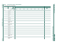
Revision history
Rev Date Description
4.1 20120820
• Table 5 and Table 127; updated reset value of DEECON register.
4 20101014
• Section 2.3; updated oscillator information.
• Section 16.1; updated oscillator information.
• Section 16.3; updated oscillator information.
• Section 16.5; updated oscillator information.
• Section 18; corrected data EEPROM row fill information.
• Table 11; updated oscillator information.
• Table 124; updated oscillator information.
3 20090617 Added information for the P89LPC9361 device.
2 20090505 Added information for the P89LPC9331 and P89LPC9341 devices.
1 20081118 Initial version.

UM10308 All information provided in this document is subject to legal disclaimers. © NXP B.V. 2012. All rights reserved.
User manual Rev. 4.1 — 20 August 2012 3 of 163
NXP Semiconductors
UM10308
P89LPC9331/9341/9351/9361 user manual
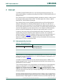
1. Introduction
The P89LPC9331/9341/9351/9361 are single-chip microcontrollers designed for
applications demanding high-integration, low cost solutions over a wide range of
performance requirements. The P89LPC9331/9341/9351/9361 are based on a high
performance processor architecture that executes instructions in two to four clocks, six
times the rate of standard 80C51 devices. Many system-level functions have been
incorporated into the P89LPC9331/9341/9351/9361 in order to reduce component count,
board space, and system cost.
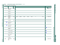
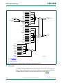
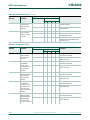
1.1 Pin configuration
Table 1. Product comparison overview
Device Flash
Memory
Sector
size
ADC1 ADC0 PGA0 PGA1 Temp
Sensor
CCU DATA
EEPROM
P89LPC9331 4 kB 1 kB X X - - X - -
P89LPC9341 4 kB 1 kB X X - - X - -
P89LPC93518kB1 kBXXXXXXX
P89LPC936116kB1 kBXXXXXXX
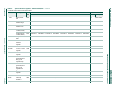
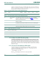
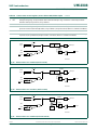
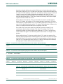
Fig 1. P89LPC9331/9341 TSSOP28 pin configuration
P89LPC9331FDH/
P89LPC9341FDH
002aae462
1
2
3
4
5
6
7
8
9
10
11
12
13
14
16
15
18
17
20
19
22
21
24
23
26
25
28
27
P2.0/AD03/DAC0
P2.1/AD02
P0.0/CMP2/KBI0/AD01
P1.7/AD00
P1.6
P1.5/RST
V
SS
P3.1/XTAL1
P3.0/XTAL2/CLKOUT
P1.4/INT1
P1.3/INT0/SDA
P1.2/T0/SCL
P2.2/MOSI
P2.3/MISO
P2.7
P2.6
P0.1/CIN2B/KBI1/AD10
P0.2/CIN2A/KBI2/AD11
P0.3/CIN1B/KBI3/AD12
P0.4/CIN1A/KBI4/DAC1/AD13
P0.5/CMPREF/KBI5
V
DD
P0.6/CMP1/KBI6
P0.7/T1/KBI7
P1.0/TXD
P1.1/RXD
P2.5/SPICLK
P2.4/SS

UM10308 All information provided in this document is subject to legal disclaimers. © NXP B.V. 2012. All rights reserved.
User manual Rev. 4.1 — 20 August 2012 4 of 163
NXP Semiconductors
UM10308
P89LPC9331/9341/9351/9361 user manual
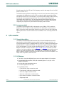
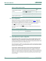
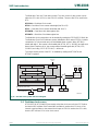
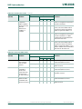
Fig 2. P89LPC9351/9361 TSSOP28 pin configuration
Fig 3. PLCC28 pin configuration
P89LPC9351FDH/
P89LPC9361FDH
002aad557
1
2
3
4
5
6
7
8
9
10
11
12
13
14
16
15
18
17
20
19
22
21
24
23
26
25
28
27
P2.0/ICB/DAC0/AD03
P2.1/OCD/AD02
P0.0/CMP2/KBI0/AD01
P1.7/OCC/AD00
P1.6/OCB
P1.5/RST
V
SS
P3.1/XTAL1
P3.0/XTAL2/CLKOUT
P1.4/INT1
P1.3/INT0/SDA
P1.2/T0/SCL
P2.2/MOSI
P2.3/MISO
P2.7/ICA
P2.6/OCA
P0.1/CIN2B/KBI1/AD10
P0.2/CIN2A/KBI2/AD11
P0.3/CIN1B/KBI3/AD12
P0.4/CIN1A/KBI4/DAC1/AD13
P0.5/CMPREF/KBI5
V
DD
P0.6/CMP1/KBI6
P0.7/T1/KBI7
P1.0/TXD
P1.1/RXD
P2.5/SPICLK
P2.4/SS
P89LPC9351FA
002aad558
5
6
7
8
9
10
11
25
24
23
22
21
20
19
12
13
14
15
16
17
18
4
3
2
1
28
27
26
P1.6/OCB
P1.5/RST
V
SS
P3.1/XTAL1
P3.0/XTAL2/CLKOUT
P1.4/INT1
P1.3/INT0/SDA
P1.7/OCC/AD00
P0.0/CMP2/KBI0/AD01
P2.1/OCD/AD02
P2.0/ICB/DAC0/AD03
P2.7/ICA
P2.6/OCA
P0.1/CIN2B/KBI1/AD10
P0.2/CIN2A/KBI2/AD11
P0.3/CIN1B/KBI3/AD12
P0.4/CIN1A/KBI4/DAC1/AD13
P0.5/CMPREF/KBI5
V
DD
P0.6/CMP1/KBI6
P0.7/T1/KBI7
P1.2/T0/SCL
P2.2/MOSI
P2.3/MISO
P2.4/SS
P2.5/SPICLK
P1.1/RXD
P1.0/TXD

UM10308 All information provided in this document is subject to legal disclaimers. © NXP B.V. 2012. All rights reserved.
User manual Rev. 4.1 — 20 August 2012 5 of 163
NXP Semiconductors
UM10308
P89LPC9331/9341/9351/9361 user manual
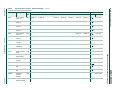
1.2 Pin description
Table 2. Pin description
Symbol Pin Type Description
PLCC28,
TSSOP28
P0.0 to P0.7 I/O Port 0: Port 0 is an 8-bit I/O port with a user-configurable output type. During reset
Port 0 latches are configured in the input only mode with the internal pull-up
disabled. The operation of Port 0 pins as inputs and outputs depends upon the port
configuration selected. Each port pin is configured independently. Refer to Section
5.1 “Port configurations” for details.
The Keypad Interrupt feature operates with Port 0 pins.
All pins have Schmitt trigger inputs.
Port 0 also provides various special functions as described below:
P0.0/CMP2/
KBI0/AD01
3I/OP0.0 — Port 0 bit 0.
O CMP2 — Comparator 2 output
I KBI0 — Keyboard input 0.
I AD01 — ADC0 channel 1 analog input.
P0.1/CIN2B/
KBI1/AD10
26 I/O P0.1 — Port 0 bit 1.
I CIN2B — Comparator 2 positive input B.
I KBI1 — Keyboard input 1.
I AD10 — ADC1 channel 0 analog input.
P0.2/CIN2A/
KBI2/AD11
25 I/O P0.2 — Port 0 bit 2.
I CIN2A — Comparator 2 positive input A.
I KBI2 — Keyboard input 2.
I AD11 — ADC1 channel 1 analog input.
P0.3/CIN1B/
KBI3/AD12
24 I/O P0.3 — Port 0 bit 3. High current source.
I CIN1B — Comparator 1 positive input B.
I KBI3 — Keyboard input 3.
I AD12 — ADC1 channel 2 analog input.
P0.4/CIN1A/
KBI4/DAC1/AD13
23 I/O P0.4 — Port 0 bit 4. High current source.
I CIN1A — Comparator 1 positive input A.
I KBI4 — Keyboard input 4.
O DAC1 — Digital-to-analog converter output 1.
I AD13 — ADC1 channel 3 analog input.
P0.5/CMPREF/
KBI5
22 I/O P0.5 — Port 0 bit 5. High current source.
I CMPREF — Comparator reference (negative) input.
I KBI5 — Keyboard input 5.
P0.6/CMP1/KBI6 20 I/O P0.6 — Port 0 bit 6. High current source.
O CMP1 — Comparator 1 output.
I KBI6 — Keyboard input 6.
P0.7/T1/KBI7 19 I/O P0.7 — Port 0 bit 7. High current source.
I/O
T1 — T
imer/counter 1 external count input or overflow output.
I KBI7 — Keyb
oard input 7.

UM10308 All information provided in this document is subject to legal disclaimers. © NXP B.V. 2012. All rights reserved.
User manual Rev. 4.1 — 20 August 2012 6 of 163
NXP Semiconductors
UM10308
P89LPC9331/9341/9351/9361 user manual
P1.0 to P1.7 I/O, I
[1]
Port 1: Port 1 is an 8-bit I/O port with a user-configurable output type, except for
three pins as noted below. During reset Port 1 latches are configured in the input
only mode with the internal pull-up disabled. The operation of the configurable
Port 1 pins as inputs and outputs depends upon the port configuration selected.
Each of the configurable port pins are programmed independently. Refer to
Section 5.1 “
Port configurations” for details. P1.2 to P1.3 are open drain when
used as outputs. P1.5 is input only.
All pins have Schmitt trigger inputs.
Port 1 also provides various special functions as described below:
P1.0/TXD 18 I/O P1.0 — Port 1 bit 0.
O TXD — Transmitter output for serial port.
P1.1/RXD 17 I/O P1.1 — Port 1 bit 1.
I RXD — Receiver input for serial port.
P1.2/T0/SCL 12 I/O P1.2 — Port 1 bit 2 (open-drain when used as output).
I/O T0 — Timer/counter 0 external count input or overflow output (open-drain when
used as output).
I/O SCL — I
2
C-bus serial clock input/output.
P1.3/INT0
/SDA 11 I/O P1.3 — Port 1 bit 3 (open-drain when used as output).
I INT0
— External interrupt 0 input.
I/O SDA — I
2
C-bus serial data input/output.
P1.4/INT1
10 I/O P1.4 — Port 1 bit 4. High current source.
I INT1
— External interrupt 1 input.
P1.5/RST
6IP1.5 — Port 1 bit 5 (input only).
I RST
— External Reset input during power-on or if selected via UCFG1. When
functioning as a reset input, a LOW on this pin resets the microcontroller, causing
I/O ports and peripherals to take on their default states, and the processor begins
execution at address 0. Also used during a power-on sequence to force ISP mode.
P1.6/OCB 5 I/O P1.6 — Port 1 bit 6. High current source.
O OCB — Output Compare B. (P89LPC9351/9361)
P1.7/OCC/AD00 4 I/O P1.7 — Port 1 bit 7. High current source.
O OCC — Output Compare C. (P89LPC9351/9361)
I AD00 — ADC0 channel 0 analog input.
P2.0 to P2.7 I/O Port 2: Port 2 is an 8-bit I/O port with a user-configurable output type. During reset
Port 2 latches are configured in the input only mode with the internal pull-up
disabled. The operation of Port 2 pins as inputs and outputs depends upon the port
configuration selected. Each port pin is configured independently. Refer to Section
5.1 “Port configurations” for details.
All pins have Schmitt trigger inputs.
Port 2 also provides various special functions as described below:
P2.0/ICB/DAC0
/AD03
1I/OP2.0 — Port 2 bit 0.
I ICB — Input Capture B. (P89LPC9351/9361)
O DAC0 — Digital-to-analog converter output.
I AD03 — ADC0 channel 3 analog input.
Table 2. Pin description
…continued
Symbol Pin Type Description
PLCC28,
TSSOP28

UM10308 All information provided in this document is subject to legal disclaimers. © NXP B.V. 2012. All rights reserved.
User manual Rev. 4.1 — 20 August 2012 7 of 163
NXP Semiconductors
UM10308
P89LPC9331/9341/9351/9361 user manual
[1] Input/output for P1.0 to P1.4, P1.6, P1.7. Input for P1.5.
P2.1/OCD/AD02 2 I/O P2.1 — Port 2 bit 1.
O OCD — Output Compare D. (P89LPC9351/9361)
I AD02 — ADC0 channel 2 analog input.
P2.2/MOSI 13 I/O P2.2 — Port 2 bit 2.
I/O MOSI — SPI master out slave in. When configured as master, this pin is output;
when configured as slave, this pin is input.
P2.3/MISO 14 I/O P2.3 — Port 2 bit 3.
I/O MISO — When configured as master, this pin is input, when configured as slave,
this pin is output.
P2.4/SS
15 I/O P2.4 — Port 2 bit 4.
I SS
— SPI Slave select.
P2.5/SPICLK 16 I/O P2.5 — Port 2 bit 5.
I/O SPICLK — SPI clock. When configured as master, this pin is output; when
configured as slave, this pin is input.
P2.6/OCA 27 I/O P2.6 — Port 2 bit 6.
O OCA — Output Compare A. (P89LPC9351/9361)
P2.7/ICA 28 I/O P2.7 — Port 2 bit 7.
I ICA — Input Capture A. (P89LPC9351/9361)
P3.0 to P3.1 I/O Port 3: Port 3 is a 2-bit I/O port with a user-configurable output type. During reset
Port 3 latches are configured in the input only mode with the internal pull-up
disabled. The operation of Port 3 pins as inputs and outputs depends upon the port
configuration selected. Each port pin is configured independently. Refer to Section
5.1 “Port configurations” for details.
All pins have Schmitt trigger inputs.
Port 3 also provides various special functions as described below:
P3.0/XTAL2/
CLKOUT
9I/OP3.0 — Port 3 bit 0.
O XTAL2 — Output from the oscillator amplifier (when a crystal oscillator option is
selected via the flash configuration.
O CLKOUT — CPU clock divided by 2 when enabled via SFR bit (ENCLK -TRIM.6).
It can be used if the CPU clock is the internal RC oscillator, watchdog oscillator or
external clock input, except when XTAL1/XTAL2 are used to generate clock source
for the RTC/system timer.
P3.1/XTAL1 8 I/O P3.1 — Port 3 bit 1.
I XTAL1 — Input to the oscillator circuit and internal clock generator circuits (when
selected via the flash configuration). It can be a port pin if internal RC oscillator or
watchdog oscillator is used as the CPU clock source, and if XTAL1/XTAL2 are not
used to generate the clock for the RTC/system timer.
V
SS
7IGround: 0 V reference.
V
DD
21 I Power supply: This is the power supply voltage for normal operation as well as
Idle and Power-down modes.
Table 2. Pin description
…continued
Symbol Pin Type Description
PLCC28,
TSSOP28

UM10308 All information provided in this document is subject to legal disclaimers. © NXP B.V. 2012. All rights reserved.
User manual Rev. 4.1 — 20 August 2012 8 of 163
NXP Semiconductors
UM10308
P89LPC9331/9341/9351/9361 user manual
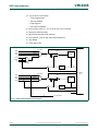
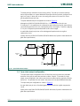
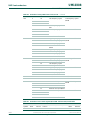
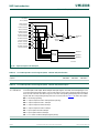
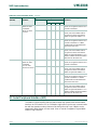
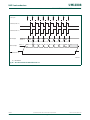
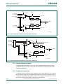
1.3 Functional diagram
Fig 4. Functional diagram (P89LPC9331/9341)
V
DD
V
SS
PORT 0
PORT 3
TXD
RXD
T0
INT0
INT1
RST
SCL
SDA
002aae461
CMP2
CIN2B
CIN2A
CIN1B
CIN1A
CMPREF
CMP1
T1
XTAL2
XTAL1
KBI0
KBI1
KBI2
KBI3
KBI4
KBI5
KBI6
KBI7
DAC1
MOSI
MISO
SS
SPICLK
AD10
AD11
AD12
AD13
AD01
PORT 1
AD00
PORT 2
P89LPC9331/
P89LPC9341
AD03
AD02
DAC0
CLKOUT
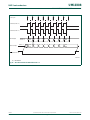
Fig 5. Functional diagram (P89LPC9351/9361)
V
DD
V
SS
PORT 0
PORT 3
TXD
RXD
T0
INT0
INT1
RST
SCL
SDA
002aad556
CMP2
CIN2B
CIN2A
CIN1B
CIN1A
CMPREF
CMP1
T1
XTAL2
XTAL1
KBI0
KBI1
KBI2
KBI3
KBI4
KBI5
KBI6
KBI7
DAC1
MOSI
MISO
SS
SPICLK
AD10
AD11
AD12
AD13
AD01
PORT 1
PORT 2
P89LPC9351/
P89LPC9361
OCB
OCC
ICB
OCD
OCA
ICA
AD00
AD03
AD02
DAC0
CLKOUT

UM10308 All information provided in this document is subject to legal disclaimers. © NXP B.V. 2012. All rights reserved.
User manual Rev. 4.1 — 20 August 2012 9 of 163
NXP Semiconductors
UM10308
P89LPC9331/9341/9351/9361 user manual
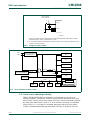
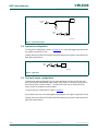
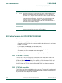
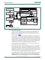
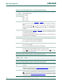
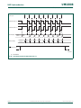
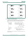
1.4 Block diagram
(1) P89LPC9351/9361
(2) PGA1 on P89LPC9351/9361
(3) PGA0 on P89LPC9351/9361
Fig 6. Block diagram
ACCELERATED 2-CLOCK 80C51 CPU
4 kB/8 kB/16 kB
CODE FLASH
256-BYTE
DATA RAM
PORT 2
CONFIGURABLE I/Os
PORT 1
CONFIGURABLE I/Os
PORT 0
CONFIGURABLE I/Os
KEYPAD
INTERRUPT
PROGRAMMABLE
OSCILLATOR DIVIDER
CPU
clock
CONFIGURABLE
OSCILLATOR
ON-CHIP RC
OSCILLATOR
WITH CLOCK
DOUBLER
internal bus
POWER MONITOR
(POWER-ON RESET,
BROWNOUT RESET)
002aad555
UART
ANALOG
COMPARATORS
512-BYTE
AUXILIARY RAM
(1)
I
2
C-BUS
512-BYTE
DATA EEPROM
(1)
PORT 3
CONFIGURABLE I/Os
CCU (CAPTURE/
COMPARE UNIT)
(1)
P89LPC9331/9341/9351/9361
WATCHDOG TIMER
AND OSCILLATOR
TIMER 0
TIMER 1
REAL-TIME CLOCK/
SYSTEM TIMER
SPI
ADC1/DAC1
(2)
ADC0/TEMP
SENSOR/DAC0
(3)
P3[1:0]
P2[7:0]
P1[7:0]
P0[7:0]
TXD
RXD
SCL
SDA
T0
T1
CMP2
CIN2B
CIN2A
CMP1
CIN1A
CIN1B
OCA
OCB
OCC
OCD
ICA
AD10
AD11
AD12
AD13
DAC1
AD00
AD01
AD02
AD03
DAC0
ICB
SPICLK
MOSI
MISO
SS
CRYSTAL
OR
RESONATOR
XTAL2
XTAL1

UM10308 All information provided in this document is subject to legal disclaimers. © NXP B.V. 2012. All rights reserved.
User manual Rev. 4.1 — 20 August 2012 10 of 163
NXP Semiconductors
UM10308
P89LPC9331/9341/9351/9361 user manual
1.5 Special function registers
Remark: SFR accesses are restricted in the following ways:
• User must not attempt to access any SFR locations not defined.
• Accesses to any defined SFR locations must be strictly for the functions for the SFRs.
• SFR bits labeled ‘-’, ‘0’ or ‘1’ can only be written and read as follows:
– ‘-’ Unless otherwise specified, must be written with ‘0’, but can return any value
when read (even if it was written with ‘0’). It is a reserved bit and may be used in
future derivatives.
– ‘0’ must be written with ‘0’, and will return a ‘0’ when read.
– ‘1’ must be written with ‘1’, and will return a ‘1’ when read.

xxxxxxxxxxxxxxxxxxxxx xxxxxxxxxxxxxxxxxxxxxxxxxx xxxxxxx x x x xxxxxxxxxxxxxxxxxxxxxxxxxxxxxx xxxxxxxxxxxxxxxxxxx xx xx xxxxx
xxxxxxxxxxxxxxxxxxxxxxxxxxx xxxxxxxxxxxxxxxxxxx xxxxxx xxxxxxxxxxxxxxxxxxxxxxxxxxxxxxxxxxx xxxxxxxxxxxx x x
xxxxxxxxxxxxxxxxxxxxx xxxxxxxxxxxxxxxxxxxxxxxxxxxxxx xxxxx xxxxxxxxxxxxxxxxxxxxxxxxxxxxxxxxxxxxxxxxxxxxxxxxxx xxxxxxxx
xxxxxxxxxxxxxxxxxxxxxxxxx xxxxxxxxxxxxxxxxxxxx xxx
UM10308 All information provided in this document is subject to legal disclaimers. © NXP B.V. 2012. All rights reserved.
User manual Rev. 4.1 — 20 August 2012 11 of 163
NXP Semiconductors
UM10308
P89LPC9331/9341/9351/9361 user manual
Table 3. Special function registers - P89LPC9331/9341
* indicates SFRs that are bit addressable.
Name Description SFR
addr.
Bit functions and addresses Reset value
MSB LSB Hex Binary
Bit address E7 E6 E5 E4 E3 E2 E1 E0
ACC* Accumulator E0H 00 0000 0000
ADCON0 A/D control
register 0
8EH ENBI0 ENADCI0 TMM0 EDGE0 ADCI0 ENADC0 ADCS01 ADCS00 00 0000 0000
ADCON1 A/D control
register 1
97H ENBI1 ENADCI1 TMM1 EDGE1 ADCI1 ENADC1 ADCS11 ADCS10 00 0000 0000
ADINS A/D input
select
A3H ADI13 ADI12 ADI11 ADI10 ADI03 ADI02 ADI01 ADI00 00 0000 0000
ADMODA A/D mode
register A
C0H BNDI1 BURST1 SCC1 SCAN1 BNDI0 BURST0 SCC0 SCAN0 00 0000 0000
ADMODB A/D mode
register B
A1H CLK2 CLK1 CLK0 INBND0 ENDAC1 ENDAC0 BSA1 BSA0 00 000x 0000
AD0BH A/D_0
boundary high
register
BBH FF 1111 1111
AD0BL A/D_0
boundary low
register
A6H 00 0000 0000
AD0DAT0 A/D_0 data
register 0
C5H 00 0000 0000
AD0DAT1 A/D_0 data
register 1
C6H 00 0000 0000
AD0DAT2 A/D_0 data
register 2
C7H 00 0000 0000
AD0DAT3 A/D_0 data
register 3
F4H 00 0000 0000
AD1BH A/D_1
boundary high
register
C4H FF 1111 1111
AD1BL A/D_1
boundary low
register
BCH 00 0000 0000

xxxxxxxxxxxxxxxxxxxxx xxxxxxxxxxxxxxxxxxxxxxxxxx xxxxxxx x x x xxxxxxxxxxxxxxxxxxxxxxxxxxxxxx xxxxxxxxxxxxxxxxxxx xx xx xxxxx
xxxxxxxxxxxxxxxxxxxxxxxxxxx xxxxxxxxxxxxxxxxxxx xxxxxx xxxxxxxxxxxxxxxxxxxxxxxxxxxxxxxxxxx xxxxxxxxxxxx x x
xxxxxxxxxxxxxxxxxxxxx xxxxxxxxxxxxxxxxxxxxxxxxxxxxxx xxxxx xxxxxxxxxxxxxxxxxxxxxxxxxxxxxxxxxxxxxxxxxxxxxxxxxx xxxxxxxx
xxxxxxxxxxxxxxxxxxxxxxxxx xxxxxxxxxxxxxxxxxxxx xxx
UM10308 All information provided in this document is subject to legal disclaimers. © NXP B.V. 2012. All rights reserved.
User manual Rev. 4.1 — 20 August 2012 12 of 163
NXP Semiconductors
UM10308
P89LPC9331/9341/9351/9361 user manual
AD1DAT0 A/D_1 data
register 0
D5H 00 0000 0000
AD1DAT1 A/D_1 data
register 1
D6H 00 0000 0000
AD1DAT2 A/D_1 data
register 2
D7H 00 0000 0000
AD1DAT3 A/D_1 data
register 3
F5H 00 0000 0000
AUXR1 Auxiliary
function
register
A2H CLKLP EBRR ENT1 ENT0 SRST 0 - DPS 00 0000 00x0
Bit address F7 F6 F5 F4 F3 F2 F1 F0
B* B register F0H 00 0000 0000
BRGR0
[2]
Baud rate
generator 0
rate low
BEH 00 0000 0000
BRGR1
[2]
Baud rate
generator 0
rate high
BFH 00 0000 0000
BRGCON Baud rate
generator 0
control
BDH------SBRGSBRGEN00
[2]
xxxx xx00
CMP1 Comparator 1
control register
ACH - - CE1 CP1 CN1 OE1 CO1 CMF1 00
[1]
xx00 0000
CMP2 Comparator 2
control register
ADH - - CE2 CP2 CN2 OE2 CO2 CMF2 00
[1]
xx00 0000
DIVM CPU clock
divide-by-M
control
95H 00 0000 0000
DPTR Data pointer
(2 bytes)
DPH Data pointer
high
83H 00 0000 0000
Table 3. Special function registers - P89LPC9331/9341
…continued
* indicates SFRs that are bit addressable.
Name Description SFR
addr.
Bit functions and addresses Reset value
MSB LSB Hex Binary

xxxxxxxxxxxxxxxxxxxxx xxxxxxxxxxxxxxxxxxxxxxxxxx xxxxxxx x x x xxxxxxxxxxxxxxxxxxxxxxxxxxxxxx xxxxxxxxxxxxxxxxxxx xx xx xxxxx
xxxxxxxxxxxxxxxxxxxxxxxxxxx xxxxxxxxxxxxxxxxxxx xxxxxx xxxxxxxxxxxxxxxxxxxxxxxxxxxxxxxxxxx xxxxxxxxxxxx x x
xxxxxxxxxxxxxxxxxxxxx xxxxxxxxxxxxxxxxxxxxxxxxxxxxxx xxxxx xxxxxxxxxxxxxxxxxxxxxxxxxxxxxxxxxxxxxxxxxxxxxxxxxx xxxxxxxx
xxxxxxxxxxxxxxxxxxxxxxxxx xxxxxxxxxxxxxxxxxxxx xxx
UM10308 All information provided in this document is subject to legal disclaimers. © NXP B.V. 2012. All rights reserved.
User manual Rev. 4.1 — 20 August 2012 13 of 163
NXP Semiconductors
UM10308
P89LPC9331/9341/9351/9361 user manual
DPL Data pointer
low
82H 00 0000 0000
FMADRH Program flash
address high
E7H 00 0000 0000
FMADRL Program flash
address low
E6H 00 0000 0000
FMCON Program flash
control (Read)
E4H BUSY - - - HVA HVE SV OI 70 0111 0000
Program flash
control (Write)
E4H FMCMD.7 FMCMD.6 FMCMD.5 FMCMD.4 FMCMD.3 FMCMD.2 FMCMD.1 FMCMD.0
FMDATA Program flash
data
E5H 00 0000 0000
I2ADR I
2
C-bus slave
address
register
DBH I2ADR.6 I2ADR.5 I2ADR.4 I2ADR.3 I2ADR.2 I2ADR.1 I2ADR.0 GC 00 0000 0000
Bit address DF DE DD DC DB DA D9 D8
I2CON* I
2
C-bus control
register
D8H - I2EN STA STO SI AA - CRSEL 00 x000 00x0
I2DAT I
2
C-bus data
register
DAH
I2SCLH Serial clock
generator/SCL
duty cycle
register high
DDH 00 0000 0000
I2SCLL Serial clock
generator/SCL
duty cycle
register low
DCH 00 0000 0000
I2STAT I
2
C-bus status
register
D9H STA.4 STA.3 STA.2 STA.1 STA.0 0 0 0 F8 11111000
Bit address AF AE AD AC AB AA A9 A8
IEN0* Interrupt
enable 0
A8H EA EWDRT EBO ES/ESR ET1 EX1 ET0 EX0 00 0000 0000
Bit address EF EE ED EC EB EA E9 E8
Table 3. Special function registers - P89LPC9331/9341
…continued
* indicates SFRs that are bit addressable.
Name Description SFR
addr.
Bit functions and addresses Reset value
MSB LSB Hex Binary

xxxxxxxxxxxxxxxxxxxxx xxxxxxxxxxxxxxxxxxxxxxxxxx xxxxxxx x x x xxxxxxxxxxxxxxxxxxxxxxxxxxxxxx xxxxxxxxxxxxxxxxxxx xx xx xxxxx
xxxxxxxxxxxxxxxxxxxxxxxxxxx xxxxxxxxxxxxxxxxxxx xxxxxx xxxxxxxxxxxxxxxxxxxxxxxxxxxxxxxxxxx xxxxxxxxxxxx x x
xxxxxxxxxxxxxxxxxxxxx xxxxxxxxxxxxxxxxxxxxxxxxxxxxxx xxxxx xxxxxxxxxxxxxxxxxxxxxxxxxxxxxxxxxxxxxxxxxxxxxxxxxx xxxxxxxx
xxxxxxxxxxxxxxxxxxxxxxxxx xxxxxxxxxxxxxxxxxxxx xxx
UM10308 All information provided in this document is subject to legal disclaimers. © NXP B.V. 2012. All rights reserved.
User manual Rev. 4.1 — 20 August 2012 14 of 163
NXP Semiconductors
UM10308
P89LPC9331/9341/9351/9361 user manual
IEN1* Interrupt
enable 1
E8H EAD EST - - ESPI EC EKBI EI2C 00
[1]
00x0 0000
Bit address BF BE BD BC BB BA B9 B8
IP0* Interrupt
priority 0
B8H - PWDRT PBO PS/PSR PT1 PX1 PT0 PX0 00
[1]
x000 0000
IP0H Interrupt
priority 0 high
B7H - PWDRTH PBOH PSH/
PSRH
PT1H PX1H PT0H PX0H 00
[1]
x000 0000
Bit address FF FE FD FC FB FA F9 F8
IP1* Interrupt
priority 1
F8H PAD PST - - PSPI PC PKBI PI2C 00
[1]
00x0 0000
IP1H Interrupt
priority 1 high
F7H PADH PSTH - - PSPIH PCH PKBIH PI2CH 00
[1]
00x0 0000
KBCON Keypad control
register
94H------PATN
_SEL
KBIF 00
[1]
xxxx xx00
KBMASK Keypad
interrupt mask
register
86H 00 0000 0000
KBPATN Keypad pattern
register
93H FF 1111 1111
Bit address 87 86 85 84 83 82 81 80
P0* Port 0 80H T1/KB7 CMP1
/KB6
CMPREF
/KB5
CIN1A
/KB4
CIN1B
/KB3
CIN2A
/KB2
CIN2B
/KB1
CMP2
/KB0
[1]
Bit address 97 96 95 94 93 92 91 90
P1* Port 1 90H - - RST
INT1 INT0/SDA T0/SCL RXD TXD
[1]
Bit address A7 A6 A5 A4 A3 A2 A1 A0
P2* Port 2 A0H - - SPICLK SS
MISO MOSI - -
[1]
Bit address B7 B6 B5 B4 B3 B2 B1 B0
P3*Port3B0H------XTAL1XTAL2
[1]
P0M1 Port 0 output
mode 1
84H (P0M1.7) (P0M1.6) (P0M1.5) (P0M1.4) (P0M1.3) (P0M1.2) (P0M1.1) (P0M1.0) FF
[1]
1111 1111
P0M2 Port 0 output
mode 2
85H (P0M2.7) (P0M2.6) (P0M2.5) (P0M2.4) (P0M2.3) (P0M2.2) (P0M2.1) (P0M2.0) 00
[1]
0000 0000
Table 3. Special function registers - P89LPC9331/9341
…continued
* indicates SFRs that are bit addressable.
Name Description SFR
addr.
Bit functions and addresses Reset value
MSB LSB Hex Binary

xxxxxxxxxxxxxxxxxxxxx xxxxxxxxxxxxxxxxxxxxxxxxxx xxxxxxx x x x xxxxxxxxxxxxxxxxxxxxxxxxxxxxxx xxxxxxxxxxxxxxxxxxx xx xx xxxxx
xxxxxxxxxxxxxxxxxxxxxxxxxxx xxxxxxxxxxxxxxxxxxx xxxxxx xxxxxxxxxxxxxxxxxxxxxxxxxxxxxxxxxxx xxxxxxxxxxxx x x
xxxxxxxxxxxxxxxxxxxxx xxxxxxxxxxxxxxxxxxxxxxxxxxxxxx xxxxx xxxxxxxxxxxxxxxxxxxxxxxxxxxxxxxxxxxxxxxxxxxxxxxxxx xxxxxxxx
xxxxxxxxxxxxxxxxxxxxxxxxx xxxxxxxxxxxxxxxxxxxx xxx
UM10308 All information provided in this document is subject to legal disclaimers. © NXP B.V. 2012. All rights reserved.
User manual Rev. 4.1 — 20 August 2012 15 of 163
NXP Semiconductors
UM10308
P89LPC9331/9341/9351/9361 user manual
P1M1 Port 1 output
mode 1
91H (P1M1.7) (P1M1.6) - (P1M1.4) (P1M1.3) (P1M1.2) (P1M1.1) (P1M1.0) D3
[1]
11x1 xx11
P1M2 Port 1 output
mode 2
92H (P1M2.7) (P1M2.6) - (P1M2.4) (P1M2.3) (P1M2.2) (P1M2.1) (P1M2.0) 00
[1]
00x0 xx00
P2M1 Port 2 output
mode 1
A4H (P2M1.7) (P2M1.6) (P2M1.5) (P2M1.4) (P2M1.3) (P2M1.2) (P2M1.1) (P2M1.0) FF
[1]
1111 1111
P2M2 Port 2 output
mode 2
A5H (P2M2.7) (P2M2.6) (P2M2.5) (P2M2.4) (P2M2.3) (P2M2.2) (P2M2.1) (P2M2.0) 00
[1]
0000 0000
P3M1 Port 3 output
mode 1
B1H------(P3M1.1)(P3M1.0)03
[1]
xxxx xx11
P3M2 Port 3 output
mode 2
B2H------(P3M2.1)(P3M2.0)00
[1]
xxxx xx00
PCON Power control
register
87H SMOD1 SMOD0 - BOI GF1 GF0 PMOD1 PMOD0 00 0000 0000
PCONA Power control
register A
B5H RTCPD - VCPD ADPD I2PD SPPD SPD - 00
[1]
0000 0000
Bit address D7 D6 D5 D4 D3 D2 D1 D0
PSW* Program status
word
D0H CY AC F0 RS1 RS0 OV F1 P 00 0000 0000
PT0AD Port 0 digital
input disable
F6H - - PT0AD.5 PT0AD.4 PT0AD.3 PT0AD.2 PT0AD.1 - 00 xx00 000x
RSTSRC Reset source
register
DFH - BOIF BOF POF R_BK R_WD R_SF R_EX
[3]
RTCCON RTC control D1H RTCF RTCS1 RTCS0 - - - ERTC RTCEN 60
[1][6]
011x xx00
RTCH RTC register
high
D2H 00
[6]
0000 0000
RTCL RTC register
low
D3H 00
[6]
0000 0000
SADDR Serial port
address
register
A9H 00 0000 0000
SADEN Serial port
address enable
B9H 00 0000 0000
Table 3. Special function registers - P89LPC9331/9341 …continued
* indicates SFRs that are bit addressable.
Name Description SFR
addr.
Bit functions and addresses Reset value
MSB LSB Hex Binary

xxxxxxxxxxxxxxxxxxxxx xxxxxxxxxxxxxxxxxxxxxxxxxx xxxxxxx x x x xxxxxxxxxxxxxxxxxxxxxxxxxxxxxx xxxxxxxxxxxxxxxxxxx xx xx xxxxx
xxxxxxxxxxxxxxxxxxxxxxxxxxx xxxxxxxxxxxxxxxxxxx xxxxxx xxxxxxxxxxxxxxxxxxxxxxxxxxxxxxxxxxx xxxxxxxxxxxx x x
xxxxxxxxxxxxxxxxxxxxx xxxxxxxxxxxxxxxxxxxxxxxxxxxxxx xxxxx xxxxxxxxxxxxxxxxxxxxxxxxxxxxxxxxxxxxxxxxxxxxxxxxxx xxxxxxxx
xxxxxxxxxxxxxxxxxxxxxxxxx xxxxxxxxxxxxxxxxxxxx xxx
UM10308 All information provided in this document is subject to legal disclaimers. © NXP B.V. 2012. All rights reserved.
User manual Rev. 4.1 — 20 August 2012 16 of 163
NXP Semiconductors
UM10308
P89LPC9331/9341/9351/9361 user manual
SBUF Serial Port data
buffer register
99H xx xxxx xxxx
Bit address 9F 9E 9D 9C 9B 9A 99 98
SCON* Serial port
control
98H SM0/FE SM1 SM2 REN TB8 RB8 TI RI 00 0000 0000
SSTAT Serial port
extended
status register
BAH DBMOD INTLO CIDIS DBISEL FE BR OE STINT 00 0000 0000
SP Stack pointer 81H 07 0000 0111
SPCTL SPI control
register
E2H SSIG SPEN DORD MSTR CPOL CPHA SPR1 SPR0 04 0000 0100
SPSTAT SPI status
register
E1HSPIFWCOL------0000xxxxxx
SPDAT SPI data
register
E3H 00 0000 0000
TAMOD Timer 0 and 1
auxiliary mode
8FH - - - T1M2 - - - T0M2 00 xxx0 xxx0
Bit address 8F 8E 8D 8C 8B 8A 89 88
TCON* Timer 0 and 1
control
88H TF1 TR1 TF0 TR0 IE1 IT1 IE0 IT0 00 0000 0000
TH0 Timer 0 high 8CH 00 0000 0000
TH1 Timer 1 high 8DH 00 0000 0000
TL0 Timer 0 low 8AH 00 0000 0000
TL1 Timer 1 low 8BH 00 0000 0000
TMOD Timer 0 and 1
mode
89H T1GATE T1C/T T1M1 T1M0 T0GATE T0C/T T0M1 T0M0 00 0000 0000
TRIM Internal
oscillator trim
register
96H RCCLK ENCLK TRIM.5 TRIM.4 TRIM.3 TRIM.2 TRIM.1 TRIM.0
[5][6]
WDCON Watchdog
control register
A7H PRE2 PRE1 PRE0 - - WDRUN WDTOF WDCLK
[4][6]
Table 3. Special function registers - P89LPC9331/9341 …continued
* indicates SFRs that are bit addressable.
Name Description SFR
addr.
Bit functions and addresses Reset value
MSB LSB Hex Binary

xxxxxxxxxxxxxxxxxxxxx xxxxxxxxxxxxxxxxxxxxxxxxxx xxxxxxx x x x xxxxxxxxxxxxxxxxxxxxxxxxxxxxxx xxxxxxxxxxxxxxxxxxx xx xx xxxxx
xxxxxxxxxxxxxxxxxxxxxxxxxxx xxxxxxxxxxxxxxxxxxx xxxxxx xxxxxxxxxxxxxxxxxxxxxxxxxxxxxxxxxxx xxxxxxxxxxxx x x
xxxxxxxxxxxxxxxxxxxxx xxxxxxxxxxxxxxxxxxxxxxxxxxxxxx xxxxx xxxxxxxxxxxxxxxxxxxxxxxxxxxxxxxxxxxxxxxxxxxxxxxxxx xxxxxxxx
xxxxxxxxxxxxxxxxxxxxxxxxx xxxxxxxxxxxxxxxxxxxx xxx
UM10308 All information provided in this document is subject to legal disclaimers. © NXP B.V. 2012. All rights reserved.
User manual Rev. 4.1 — 20 August 2012 17 of 163
NXP Semiconductors
UM10308
P89LPC9331/9341/9351/9361 user manual
[1] All ports are in input only (high-impedance) state after power-up.
[2] BRGR1 and BRGR0 must only be written if BRGEN in BRGCON SFR is logic 0. If any are written while BRGEN = 1, the result is unpredictable.
[3] The RSTSRC register reflects the cause of the P89LPC9331/9341 reset except BOIF bit. Upon a power-up reset, all reset source flags are cleared except POF and BOF; the
power-on reset value is x011 0000.
[4] After reset, the value is 1110 01x1, i.e., PRE2 to PRE0 are all logic 1, WDRUN = 1 and WDCLK = 1. WDTOF bit is logic 1 after watchdog reset and is logic 0 after power-on reset.
Other resets will not affect WDTOF.
[5] On power-on reset and watchdog reset, the TRIM SFR is initialized with a factory preprogrammed value. Other resets will not cause initialization of the TRIM register.
[6] The only reset sources that affect these SFRs are power-on reset and watchdog reset.
WDL Watchdog load C1H FF 1111 1111
WFEED1 Watchdog
feed 1
C2H
WFEED2 Watchdog
feed 2
C3H
Table 3. Special function registers - P89LPC9331/9341 …continued
* indicates SFRs that are bit addressable.
Name Description SFR
addr.
Bit functions and addresses Reset value
MSB LSB Hex Binary

xxxxxxxxxxxxxxxxxxxxx xxxxxxxxxxxxxxxxxxxxxxxxxx xxxxxxx x x x xxxxxxxxxxxxxxxxxxxxxxxxxxxxxx xxxxxxxxxxxxxxxxxxx xx xx xxxxx
xxxxxxxxxxxxxxxxxxxxxxxxxxx xxxxxxxxxxxxxxxxxxx xxxxxx xxxxxxxxxxxxxxxxxxxxxxxxxxxxxxxxxxx xxxxxxxxxxxx x x
xxxxxxxxxxxxxxxxxxxxx xxxxxxxxxxxxxxxxxxxxxxxxxxxxxx xxxxx xxxxxxxxxxxxxxxxxxxxxxxxxxxxxxxxxxxxxxxxxxxxxxxxxx xxxxxxxx
xxxxxxxxxxxxxxxxxxxxxxxxx xxxxxxxxxxxxxxxxxxxx xxx
UM10308 All information provided in this document is subject to legal disclaimers. © NXP B.V. 2012. All rights reserved.
User manual Rev. 4.1 — 20 August 2012 18 of 163
NXP Semiconductors
UM10308
P89LPC9331/9341/9351/9361 user manual
[1] Extended SFRs are physically located on-chip but logically located in external data memory address space (XDATA). The MOVX A,@DPTR and MOVX @DPTR,A instructions are
used to access these extended SFRs.
[2] The BOICFG1/0 will be copied from UCFG1.5 and UCFG1.3 when power-on reset.
[3] CLKCON register reset value comes from UCFG1 and UCFG2. The reset value of CLKCON.2 to CLKCON.0 come from UCFG1.2 to UCFG1.0 and reset value of CLKDBL bit
comes from UCFG2.7.
Table 4. Extended special function registers - P89LPC9331/9341
[1]
Name Description SFR
addr.
Bit functions and addresses Reset value
MSB LSB Hex Binary
BODCFG BOD
configuration
register
FFC8H - - - - - - BOICFG1 BOICFG0
[2]
CLKCON CLOCK Control
register
FFDEH CLKOK - - XTALWD CLKDBL FOSC2 FOSC1 FOSC0
[3]
TPSCON Temperature
sensor control
register
FFCAH - - - - TSEL1 TSEL0 - - 00 0000 0000
RTCDATH Real-time clock
data register
high
FFBFH 00 0000 0000
RTCDATL Real-time clock
data register low
FFBEH 00 0000 0000

xxxxxxxxxxxxxxxxxxxxx xxxxxxxxxxxxxxxxxxxxxxxxxx xxxxxxx x x x xxxxxxxxxxxxxxxxxxxxxxxxxxxxxx xxxxxxxxxxxxxxxxxxx xx xx xxxxx
xxxxxxxxxxxxxxxxxxxxxxxxxxx xxxxxxxxxxxxxxxxxxx xxxxxx xxxxxxxxxxxxxxxxxxxxxxxxxxxxxxxxxxx xxxxxxxxxxxx x x
xxxxxxxxxxxxxxxxxxxxx xxxxxxxxxxxxxxxxxxxxxxxxxxxxxx xxxxx xxxxxxxxxxxxxxxxxxxxxxxxxxxxxxxxxxxxxxxxxxxxxxxxxx xxxxxxxx
xxxxxxxxxxxxxxxxxxxxxxxxx xxxxxxxxxxxxxxxxxxxx xxx
UM10308 All information provided in this document is subject to legal disclaimers. © NXP B.V. 2012. All rights reserved.
User manual Rev. 4.1 — 20 August 2012 19 of 163
NXP Semiconductors
UM10308
P89LPC9331/9341/9351/9361 user manual
Table 5. Special function registers - P89LPC9351/9361
* indicates SFRs that are bit addressable.
Name Description SFR
addr.
Bit functions and addresses Reset value
MSB LSB Hex Binary
Bit address E7 E6 E5 E4 E3 E2 E1 E0
ACC* Accumulator E0H 00 0000 0000
ADCON0 A/D control
register 0
8EH ENBI0 ENADCI0 TMM0 EDGE0 ADCI0 ENADC0 ADCS01 ADCS00 00 0000 0000
ADCON1 A/D control
register 1
97H ENBI1 ENADCI1 TMM1 EDGE1 ADCI1 ENADC1 ADCS11 ADCS10 00 0000 0000
ADINS A/D input select A3H ADI13 ADI12 ADI11 ADI10 ADI03 ADI02 ADI01 ADI00 00 0000 0000
ADMODA A/D mode
register A
C0H BNDI1 BURST1 SCC1 SCAN1 BNDI0 BURST0 SCC0 SCAN0 00 0000 0000
ADMODB A/D mode
register B
A1H CLK2 CLK1 CLK0 INBND0 ENDAC1 ENDAC0 BSA1 BSA0 00 000x 0000
AD0BH A/D_0 boundary
high register
BBH FF 1111 1111
AD0BL A/D_0 boundary
low register
A6H 00 0000 0000
AD0DAT0 A/D_0 data
register 0
C5H 00 0000 0000
AD0DAT1 A/D_0 data
register 1
C6H 00 0000 0000
AD0DAT2 A/D_0 data
register 2
C7H 00 0000 0000
AD0DAT3 A/D_0 data
register 3
F4H 00 0000 0000
AD1BH A/D_1 boundary
high register
C4H FF 1111 1111
AD1BL A/D_1 boundary
low register
BCH 00 0000 0000
AD1DAT0 A/D_1 data
register 0
D5H 00 0000 0000
AD1DAT1 A/D_1 data
register 1
D6H 00 0000 0000
AD1DAT2 A/D_1 data
register 2
D7H 00 0000 0000

xxxxxxxxxxxxxxxxxxxxx xxxxxxxxxxxxxxxxxxxxxxxxxx xxxxxxx x x x xxxxxxxxxxxxxxxxxxxxxxxxxxxxxx xxxxxxxxxxxxxxxxxxx xx xx xxxxx
xxxxxxxxxxxxxxxxxxxxxxxxxxx xxxxxxxxxxxxxxxxxxx xxxxxx xxxxxxxxxxxxxxxxxxxxxxxxxxxxxxxxxxx xxxxxxxxxxxx x x
xxxxxxxxxxxxxxxxxxxxx xxxxxxxxxxxxxxxxxxxxxxxxxxxxxx xxxxx xxxxxxxxxxxxxxxxxxxxxxxxxxxxxxxxxxxxxxxxxxxxxxxxxx xxxxxxxx
xxxxxxxxxxxxxxxxxxxxxxxxx xxxxxxxxxxxxxxxxxxxx xxx
UM10308 All information provided in this document is subject to legal disclaimers. © NXP B.V. 2012. All rights reserved.
User manual Rev. 4.1 — 20 August 2012 20 of 163
NXP Semiconductors
UM10308
P89LPC9331/9341/9351/9361 user manual
AD1DAT3 A/D_1 data
register 3
F5H 00 0000 0000
AUXR1 Auxiliary function
register
A2H CLKLP EBRR ENT1 ENT0 SRST 0 - DPS 00 0000 00x0
Bit address F7 F6 F5 F4 F3 F2 F1 F0
B* B register F0H 00 0000 0000
BRGR0
[2]
Baud rate
generator 0 rate
low
BEH 00 0000 0000
BRGR1
[2]
Baud rate
generator 0 rate
high
BFH 00 0000 0000
BRGCON Baud rate
generator 0
control
BDH------SBRGSBRGEN00
[2]
xxxx xx00
CCCRA Capture compare
A control register
EAH ICECA2 ICECA1 ICECA0 ICESA ICNFA FCOA OCMA1 OCMA0 00 0000 0000
CCCRB Capture compare
B control register
EBH ICECB2 ICECB1 ICECB0 ICESB ICNFB FCOB OCMB1 OCMB0 00 0000 0000
CCCRC Capture compare
C control register
ECH-----FCOCOCMC1OCMC000xxxx x000
CCCRD Capture compare
D control register
EDH-----FCODOCMD1OCMD000xxxx x000
CMP1 Comparator 1
control register
ACH - - CE1 CP1 CN1 OE1 CO1 CMF1 00
[1]
xx00 0000
CMP2 Comparator 2
control register
ADH - - CE2 CP2 CN2 OE2 CO2 CMF2 00
[1]
xx00 0000
DEECON Data EEPROM
control register
F1H EEIF HVERR ECTL1 ECTL0 - EWERR1 EWERR0 EADR8 80 1000 0000
DEEDAT Data EEPROM
data register
F2H 00 0000 0000
DEEADR Data EEPROM
address register
F3H 00 0000 0000
Table 5. Special function registers - P89LPC9351/9361
* indicates SFRs that are bit addressable.
Name Description SFR
addr.
Bit functions and addresses Reset value
MSB LSB Hex Binary
Page is loading ...
Page is loading ...
Page is loading ...
Page is loading ...
Page is loading ...
Page is loading ...
Page is loading ...
Page is loading ...
Page is loading ...
Page is loading ...
Page is loading ...
Page is loading ...
Page is loading ...
Page is loading ...
Page is loading ...
Page is loading ...
Page is loading ...
Page is loading ...
Page is loading ...
Page is loading ...
Page is loading ...
Page is loading ...
Page is loading ...
Page is loading ...
Page is loading ...
Page is loading ...
Page is loading ...
Page is loading ...
Page is loading ...
Page is loading ...
Page is loading ...
Page is loading ...
Page is loading ...
Page is loading ...
Page is loading ...
Page is loading ...
Page is loading ...
Page is loading ...
Page is loading ...
Page is loading ...
Page is loading ...
Page is loading ...
Page is loading ...
Page is loading ...
Page is loading ...
Page is loading ...
Page is loading ...
Page is loading ...
Page is loading ...
Page is loading ...
Page is loading ...
Page is loading ...
Page is loading ...
Page is loading ...
Page is loading ...
Page is loading ...
Page is loading ...
Page is loading ...
Page is loading ...
Page is loading ...
Page is loading ...
Page is loading ...
Page is loading ...
Page is loading ...
Page is loading ...
Page is loading ...
Page is loading ...
Page is loading ...
Page is loading ...
Page is loading ...
Page is loading ...
Page is loading ...
Page is loading ...
Page is loading ...
Page is loading ...
Page is loading ...
Page is loading ...
Page is loading ...
Page is loading ...
Page is loading ...
Page is loading ...
Page is loading ...
Page is loading ...
Page is loading ...
Page is loading ...
Page is loading ...
Page is loading ...
Page is loading ...
Page is loading ...
Page is loading ...
Page is loading ...
Page is loading ...
Page is loading ...
Page is loading ...
Page is loading ...
Page is loading ...
Page is loading ...
Page is loading ...
Page is loading ...
Page is loading ...
Page is loading ...
Page is loading ...
Page is loading ...
Page is loading ...
Page is loading ...
Page is loading ...
Page is loading ...
Page is loading ...
Page is loading ...
Page is loading ...
Page is loading ...
Page is loading ...
Page is loading ...
Page is loading ...
Page is loading ...
Page is loading ...
Page is loading ...
Page is loading ...
Page is loading ...
Page is loading ...
Page is loading ...
Page is loading ...
Page is loading ...
Page is loading ...
Page is loading ...
Page is loading ...
Page is loading ...
Page is loading ...
Page is loading ...
Page is loading ...
Page is loading ...
Page is loading ...
Page is loading ...
Page is loading ...
Page is loading ...
Page is loading ...
Page is loading ...
Page is loading ...
Page is loading ...
Page is loading ...
Page is loading ...
Page is loading ...
Page is loading ...
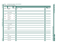
-
 1
1
-
 2
2
-
 3
3
-
 4
4
-
 5
5
-
 6
6
-
 7
7
-
 8
8
-
 9
9
-
 10
10
-
 11
11
-
 12
12
-
 13
13
-
 14
14
-
 15
15
-
 16
16
-
 17
17
-
 18
18
-
 19
19
-
 20
20
-
 21
21
-
 22
22
-
 23
23
-
 24
24
-
 25
25
-
 26
26
-
 27
27
-
 28
28
-
 29
29
-
 30
30
-
 31
31
-
 32
32
-
 33
33
-
 34
34
-
 35
35
-
 36
36
-
 37
37
-
 38
38
-
 39
39
-
 40
40
-
 41
41
-
 42
42
-
 43
43
-
 44
44
-
 45
45
-
 46
46
-
 47
47
-
 48
48
-
 49
49
-
 50
50
-
 51
51
-
 52
52
-
 53
53
-
 54
54
-
 55
55
-
 56
56
-
 57
57
-
 58
58
-
 59
59
-
 60
60
-
 61
61
-
 62
62
-
 63
63
-
 64
64
-
 65
65
-
 66
66
-
 67
67
-
 68
68
-
 69
69
-
 70
70
-
 71
71
-
 72
72
-
 73
73
-
 74
74
-
 75
75
-
 76
76
-
 77
77
-
 78
78
-
 79
79
-
 80
80
-
 81
81
-
 82
82
-
 83
83
-
 84
84
-
 85
85
-
 86
86
-
 87
87
-
 88
88
-
 89
89
-
 90
90
-
 91
91
-
 92
92
-
 93
93
-
 94
94
-
 95
95
-
 96
96
-
 97
97
-
 98
98
-
 99
99
-
 100
100
-
 101
101
-
 102
102
-
 103
103
-
 104
104
-
 105
105
-
 106
106
-
 107
107
-
 108
108
-
 109
109
-
 110
110
-
 111
111
-
 112
112
-
 113
113
-
 114
114
-
 115
115
-
 116
116
-
 117
117
-
 118
118
-
 119
119
-
 120
120
-
 121
121
-
 122
122
-
 123
123
-
 124
124
-
 125
125
-
 126
126
-
 127
127
-
 128
128
-
 129
129
-
 130
130
-
 131
131
-
 132
132
-
 133
133
-
 134
134
-
 135
135
-
 136
136
-
 137
137
-
 138
138
-
 139
139
-
 140
140
-
 141
141
-
 142
142
-
 143
143
-
 144
144
-
 145
145
-
 146
146
-
 147
147
-
 148
148
-
 149
149
-
 150
150
-
 151
151
-
 152
152
-
 153
153
-
 154
154
-
 155
155
-
 156
156
-
 157
157
-
 158
158
-
 159
159
-
 160
160
-
 161
161
-
 162
162
-
 163
163


Ask a question and I''ll find the answer in the document
Finding information in a document is now easier with AI
Related papers
Other documents
-
OKI MSM83C154S User manual
-
Lucent Technologies MN102F85K User manual
-
NXP Semiconductors P89LPC9321 UM10310 User manual
-
Atos LF050-IN Owner's manual
-
 MitraStar Technology ZMYV2ACDB100 User manual
-
 ThermoProbe TL2-A Instructions For Use Manual
-
Silicon Labs EFM8SB2 Reference guide
-
Tandy 600 Programmer's Reference Manual
-
-
 Cobalt Digital Inc 9341 User manual


