
MPC8260ESS7UMAD/D
12/2002
Rev. 0.1
Enhanced SS7
Microcode Specification
Addendum to MPC8260 RevB ROM Microcode Additions
Fr
eescale S
emiconduct
or
, I
Freescale Semiconductor, Inc.
For More Information On This Product,
Go to: www.freescale.com
nc...

Fr
eescale S
emiconduct
or
, I
Freescale Semiconductor, Inc.
For More Information On This Product,
Go to: www.freescale.com
nc...

MOTOROLA
Enhanced SS7 Microcode Specification
1
PRELIMINARY—SUBJECT TO CHANGE WITHOUT NOTICE
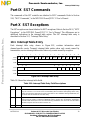
About This Document
This document describes additional functionality available only with the enhanced SS7
RAM microcode package supplement to the SS7 microcode available in ROM on the
MPC8260.
Definitions
SS7
SS7 microcode is standard on all MPC8260 devices (beginning with HiP3 Rev. B.3) and
supports MTP-2 features according to the following standards:
• ITU-T Q.703
— Section 3: Signal unit delimitation
— Section 4: Acceptance procedure
— Section 10: Signaling link error monitoring
• ANSI T1.111
• Japanese JT Q.703
Enhanced SS7
The enhanced SS7 microcode is a product (product #: MPC8260SW-ESS7) that can only
be obtained by contacting your local Motorola sales office. In addition to the above
standards, it supports the following:
• ITU-T Q.703 Annex A (provides for high speed SS7 channels at T1/E1 rates)
— Section A.1.x
— Section A.4.x
— Section A.10.x
• Chinese 2M GB standard (supports SS7 at a speed of 2Mbps for the Chinese market)
— Section 4.2.1: Signal unit delimitation and alignment
— Section 4.2.2: Error detection
— Section 4.2.5: Signalling link error monitoring
— Section 4.2.8: Signal unit format
— Section 4.2.9.8: EIM and AERM
Fr
eescale S
emiconduct
or
, I
Freescale Semiconductor, Inc.
For More Information On This Product,
Go to: www.freescale.com
nc...

2
Enhanced SS7 Microcode Specification
MOTOROLA
PRELIMINARY—SUBJECT TO CHANGE WITHOUT NOTICE
References
Dual-Port RAM Limitations
The enhanced SS7 microcode requires 8Kbyte of RAM. On MPC8260 HiP3 silicon
(beginning with Rev. B.3), this microcode package occupies the first 8Kbytes of DPRAM.
Therefore, MCC1 channels are not available.
On MPC826xA HiP4 silicon, which has an additional 32 Kbytes of DPRAM, the enhanced
SS7 microcode package does not affect MCC1 channels.
References
Users of this document should also be familiar with the following:
•
MPC8260 PowerQUICC II User’s Manual
(Doc ID: MPC8260UM/D)
— Errata to the
MPC8260 User’s Manual
(Doc ID: MPC8260UMAD/D)
•
MPC8260 RevB ROM Microcode Additions
(Doc ID: MPC8260BMCUMAD/D)
The above are available for free download. Go to www.motorola.com/semiconductors.
Document Revision History
Part I Introduction
Based on the HDLC protocol, the signalling system #7 (SS7) protocol is used to manage
public switching networks. The SS7 protocol operates on signal units (SU), which are
analogous to HDLC frames. The physical, data-link, and network-layer functions of the
SS7 protocol are collectively called the message transfer part (MTP). The enhanced SS7
microcode on the MPC8260 enables applications that require multi-channel SS7
processing.
The enhanced SS7 controller is implemented using the MCC hardware with microcode
running on the CPM. Each MCC implements the following layer 2 (data-link) functions of
the MTP:
• Signal unit (SU) retransmission
• Automatic fill-in signal unit (FISU) transmission
• Short SU filtering
• Duplicate fill-in and link-status signal unit (FISU/LSSU) filtering
• Octet counting
Document Revision Changes
0 • Initial version
0.1 • Change to description of proving in Section 7.3.4.2, “Japanese SS7:”
Fr
eescale S
emiconduct
or
, I
Freescale Semiconductor, Inc.
For More Information On This Product,
Go to: www.freescale.com
nc...

MOTOROLA
Enhanced SS7 Microcode Specification
3
PRELIMINARY—SUBJECT TO CHANGE WITHOUT NOTICE
References
• Signal unit error rate monitoring
• Extended sequence number
• errored interval monitoring
• Good frame counter and bad frame counting
• Initial alignment (Supports Alignment Error Rate Monitoring)
Note, however, that host software is needed to handle the following higher-level functions
of the MTP layer 2 not supported by the SS7 controller:
• Link state control
• Flow control
Part II Enhanced SS7 Controller Features
The primary features of the enhanced SS7 controller are as follows:
• Support for up to 4 independent channels (AnnexA/GB) on MCCs
— Refer to “Dual-Port RAM Limitations” note on page 2
• Independent mapping for receive and transmit
• Standard HDLC features
— Flag/Abort/Idle generation/detection
— Zero insertion/deletion
— 16-bit CRC-CCITT generation/checking
— Detection of non-octet aligned signal units
— Programmable number of flags between signal units
• Maintenance of errored interval monitor (EIM) (not applicable in Japanese mode)
• Maintenance of signal unit error monitor (SUERM)
• Maintenance of alignment error rate monitor (AERM)
• Maintenance of separate counters for error-free and bad frames
• Detection and stripping of long signal units
• Discard of short signal units (those that are less than 5 octets or less than 8 if
extended sequence number is used for Annex A/GB standards)
• Transmission of signal units with a programmable delay (applies to JT-Q.703
standard)
• Automatic transmission of fill-in signal units (FISU)
• Automatic retransmission of signal units (for link-status signal unit (LSSU)
retransmission)
Fr
eescale S
emiconduct
or
, I
Freescale Semiconductor, Inc.
For More Information On This Product,
Go to: www.freescale.com
nc...

4
Enhanced SS7 Microcode Specification
MOTOROLA
PRELIMINARY—SUBJECT TO CHANGE WITHOUT NOTICE
References
• Automatic discard of identical FISUs and LSSUs using a user-defined mask
• Octet counting mode in case of long signal units and receiver overrun
• Five circular interrupt tables with programmable size and overflow
identification—one for transmit and four for receive.
• Global or individual channel loop modes
• Efficient bus usage (no bus usage for inactive channels or for active channels with
nothing to send)
• Efficient control of interrupts to the CPU
• Supports external BD tables
• Uses on-chip dual-port RAM for parameter storage
• Uses 64-bit data transactions for reading and writing data in BDs
Part III SS7 Data Structure Organization
The enhanced SS7 controller uses the same data structures as MCC. Refer to Section 27.2,
“MCC Data Structures Organization,” in the
MPC8260 PowerQUICC II User’s Manual
.
Part IV Global SS7 Parameters
The global parameters of enhanced SS7 controller are identical to MCC global parameters.
Refer to Section 27.3, “Global MCC Parameters,” in the
MPC8260 PowerQUICC II User’s
Manual
.
Part V Channel Extra Parameters
The extra parameters of enhanced SS7 channels are identical to the MCC channel extra
parameters. Refer to Section 27.4, “Channel Extra Parameters,” in the
MPC8260
PowerQUICC II User’s Manual
.
Part VI Super Channel Table
The super channel table of enhanced SS7 controller is identical to MCC super channel
table. Refer to Section 27.5, “Super Channel Table,” in the
MPC8260 PowerQUICC II
User’s Manual
.
Fr
eescale S
emiconduct
or
, I
Freescale Semiconductor, Inc.
For More Information On This Product,
Go to: www.freescale.com
nc...

MOTOROLA
Enhanced SS7 Microcode Specification
5
PRELIMINARY—SUBJECT TO CHANGE WITHOUT NOTICE
References
Part VII Channel-Specific Parameters
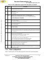
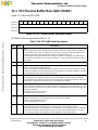
Table 7-1 describes channel-specific parameters for enhanced SS7. Note that a given
parameter location may have a different definition depending on the standard used
(ITU-T/ANSI or AnnexA/GB/Japanese standard).
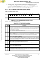
Table 7-1. Channel-Specific Parameters for SS7
Offset
1
Name
2
Width Description
0x00
TSTATE
Word Tx internal state. The user must write to TSTATE 0xHH80_0000. HH is the TSTATE
High Byte. Refer to Section 27.6.1, “Internal Transmitter State (TSTATE)” in the
MPC8260 PowerQUICC II User’s Manual
.
0x04
ZISTATE
Word Zero-insertion machine state.(User-initialized to 0x10000207 for regular channel, and
0x30000207 for reversed bit order channel).
0x08
ZIDATA0
Word Zero-insertion high word data buffer (User-initialized to 0xFFFFFFFF)
0x0C
ZIDATA1
Word Zero-insertion low word data buffer (User-initialized to 0xFFFFFFFF)
0x10 TBDFlags Hword TxBD flags. Used by the CP (read-only for the user).
0x12 TBDCNT Hword Tx internal byte count. Number of remaining bytes in buffer, used by the CP (read-only
for the user).
0x14 TBDPTR Word Tx internal data pointer. Points to current absolute data address of channel, used by
the CP (read-only for the user).
0x18
ECHAMR
Word Extended channel mode register. Refer to Section 7.1, “Extended Channel Mode
Register (ECHAMR).”
0x1C TCRC Word Temporary transmit CRC. Temporary value of CRC calculation result, used by the CP
(read-only for the user).
0x20
RSTATE
Word Rx internal state. To start a receiver channel the user must write to RSTATE
0xHH80_0000. HH is the RSTATE High Byte. Refer to Section 27.6.4, “Internal
Receiver State (RSTATE)” in the
MPC8260 PowerQUICC II User’s Manual.
0x24
ZDSTATE
Word Zero-deletion machine state (User-initialized to 0x00FFFFE0 for regular channel, and
0x20FFFFE0 for reversed bit order channel)
0x28
ZDDATA0
Word Zero-deletion high word data buffer (User-initialized to 0xFFFFFFFF)
0x2C
ZDDATA1
Word Zero-deletion low word data buffer (User-initialized to 0xFFFFFFFF)
0x30 RBDFlags Hword RxBD flags. Used by the CP (read-only for the user).
0x32 RBDCNT Hword Rx internal byte count. Number of remaining bytes in buffer, used by the CP
(read-only for the user).
0x34 RBDPTR Word Rx internal data pointer. Points to current absolute data address of channel, used by
the CP (read-only for the user).
0x38
MFLR
Hword Maximum frame length register. Defines the longest expected frame for this channel.
(64-Kbyte maximum). The remainder of a frame that is larger than MFLR is discarded
and the LG flag is set in the last frame’s BD. An interrupt request might be generated
(RXF and RXB) depending on the interrupt mask. A frame’s length is considered to
be everything between flags, including CRC. No more data is written into the current
buffer when the MFLR violation is detected.
0x3A MAX_cnt Hword Max_length counter. Used by the CP (read-only for the user).
Fr
eescale S
emiconduct
or
, I
Freescale Semiconductor, Inc.
For More Information On This Product,
Go to: www.freescale.com
nc...

6
Enhanced SS7 Microcode Specification
MOTOROLA
PRELIMINARY—SUBJECT TO CHANGE WITHOUT NOTICE
References
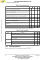
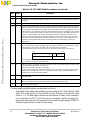
0x3C RCRC Word Temporary receive CRC. Used by the CP (read-only for the user).
0x40
N
Hword Applies to ITU-T/ANSI (including ITU-T Annex A) SS7 only. Interrupt threshold in octet
counting mode (N=16). Refer to Section 7.2, “Signal Unit Error Monitor (SUERM).”
N_cnt
Hword Applies to ITU-T/ANSI (including ITU-T Annex A) SS7 only. Temporary down counter
for N (user initialized to the value of N).
JTSTTmp Word Applies to Japanese SS7 only. Temporary storage for Time-Stamp Register Value.
Used by the CP to implement a 24-ms delay before sending FISU.
0x44
D
Hword Signal unit to signal unit error ratio (SUERM parameter, user initialized to 256). Refer
to Section 7.2, “Signal Unit Error Monitor (SUERM).” For Japanese SS7 refer to
Section 7.2.1, “SUERM in Japanese SS7.” For EIM refer to Section 7.3.2, “EIM
Implementation.”
0x46
D_cnt
Hword Applies to ITU-T/ANSI SS7 only. Temporary down-counter for D (user initialized to the
value of D). D_cnt is decremented only when receive buffers are available.
JTTDelay
Applies to Japanese SS7 only. FISU retransmission delay (specified in units of 512
µs). According to the Japanese SS7 standard, the delay should be 24 ms and thus
JTTDelay should be programmed to 24 ms/512 µs = 46.875 (approximately 47).
Hence, the user should program JTTDelay to 0x2F and the RTSCR to generate a 1
µs time stamp period. Refer to Section 13.3.7, “RISC Time-Stamp Control Register
(RTSCR),” in the
MPC8260 PowerQUICC II User’s Manual
. According to SS7 Annex
A, the delay should be cleared (0x00).
0x48
Mask1
Word Mask for SU filtering, bytes 1-4. Refer to Section 7.3.7, “SU Filtering.”
0x4C
Mask2
Hword Mask for SU filtering, byte 5-6. Refer to Section 7.3.7, “SU Filtering.
0x4E
SS7_OPT
Hword SS7 configuration register. Refer to Section 7.3, “SS7 Configuration Register
(SS7_OPT).”
0x50 LRB1_Tmp Word Temporary storage. Used by CP for SU filtering.
0x54 LRB2_Tmp Hword Temporary storage. Used by CP for SU filtering.
0x56
SUERM
Hword Signal unit error rate monitor counter (user initialized to 0). Refer to Section 7.2,
“Signal Unit Error Monitor (SUERM).” For Japanese SS7, refer toSection 7.2.1,
“SUERM in Japanese SS7.” For errored interval monitor, refer to Section 7.3.2, “EIM
Implementation.”
0x58 LRB1 Word Four first bytes of last received signal unit. Used by CP for SU filtering. Refer to
Section 7.3.7, “SU Filtering.”
0x5C LRB2 Hword Fifth and sixth byte of last received signal unit. Used by CP for SU filtering. Refer to
Section 7.3.7, “SU Filtering.”
0x5E
T
Hword SUERM threshold value (user initialized to 64 for SUERM). Refer to Section 7.2,
“Signal Unit Error Monitor (SUERM).” For Japanese SS7, refer toSection 7.2.1,
“SUERM in Japanese SS7.” For errored interval monitor, refer to Section 7.3.2, “EIM
Implementation.” For AERM refer to Section 7.3.4, “AERM Implementation.”
0x60 LHDR Word The BSN, BIB, FSN, FIB fields of last transmitted signal unit and result of CRC. Used
by CP for automatic FISU transmission.
0x64 LHDR_Tmp Word Used by CP for automatic FISU transmission.
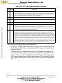
Table 7-1. Channel-Specific Parameters for SS7 (continued)
Offset
1
Name
2
Width Description
Fr
eescale S
emiconduct
or
, I
Freescale Semiconductor, Inc.
For More Information On This Product,
Go to: www.freescale.com
nc...

MOTOROLA
Enhanced SS7 Microcode Specification
7
PRELIMINARY—SUBJECT TO CHANGE WITHOUT NOTICE
Extended Channel Mode Register (ECHAMR)
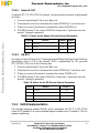
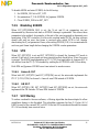
7.1 Extended Channel Mode Register (ECHAMR)
The extended channel mode register (ECHAMR) is a user-initialized register, is shown in
Figure 7-1. It includes both the interrupt mask bits and channel configuration bits.
0x68 EFSUC Word Error-free signal unit counter, user initialized to 0. The counter is incremented
whenever an error-free (no CRC error, no non-octet aligned error, no short or long
frame errors) signal unit is received.
0x6C SUEC Word Signal unit error counter, user initialized to 0. Incremented each time an SU is
received that contains an error. These errors are: short frame, long frame, CRC error,
and non-octet aligned error.
0x70 SS7STATE Word Internal state of SS7 controller. User initialized to 0.
0x74 JTSRTmp Word Used by the CP to implement signal unit error rate monitoring in Japanese SS7 and
errored interval monitoring in SS7 Annex A/GB.
0x78
JTRDelay
Hword Specified in units of 512 µs. SUERM delay in Japanese SS7 and the interval in
“errored interval monitor”; otherwise should be cleared. According to the Japanese
SS7 standard, the delay should be 24 ms and thus JTRDelay should be programmed
to 24 ms/512 µs = 46.875 (approximately 47). Hence, the user should program
JTRDelay to 0x2F and the RTSCR to generate a 1 µs time stamp period. Refer to
Section 13.3.7, “RISC Time-Stamp Control Register (RTSCR),” in the
MPC8260
PowerQUICC II User’s Manual.
For EIM, According to SS7 AnnexA/GB, the delay
should be 100ms and thus JTRDelay should be programmed to 100ms/512µs = 195.3
(approximately 195). Hence, the user should program JTRDelay to 0xC3. Refer to
Section 7.3.2, “EIM Implementation.”
0x7A
M
Hword ITU threshold for AERM. If M_cnt reaches M, an AERM interrupt is generated. Note
that M is normally programmed to 5.
0x7C
M_cnt
Hword Up-counter for M. Should be cleared during initialization.
0x7E
Mask_3
Hword Mask for SU filtering byte 7 and 8.
0x80 LRB3_Tmp Hword Temp storage for SU filtering.
0x82 LRB3 Hword Seventh and eighth byte of last received SU.
0x84
U
Hword Down counter for EIM in GB only. Refer to Section 7.3.2.2, “GB SS7.”
0x86–
0xFF
Reserved — Reserved, should be cleared.
1
The offset is relative to the dual-port RAM address + 64
x
CH_NUM.
SS7 (ITU 64k)channel specific parameters require twice the amount of dual-port RAM required for HDLC or
Transparent channel specific parameters. Therefore, for ITU 64k SS7, even channel numbers (0, 2, 4 etc.) must be
used.
Annex A/GB channel specific parameters require four times the amount of dual-port RAM required for HDLC or
Transparent channel specific parameters. Therefore, for Annex A/GB every fourth channel numbers (0, 4, 8, etc.) must
be used and all channel numbers in between must be left unused.
2
BOLD entries in the above table indicate parameters which MUST be initialized by the user. All other parameters are
managed by the microcode and should be initialized to zero unless otherwise stated.
Table 7-1. Channel-Specific Parameters for SS7 (continued)
Offset
1
Name
2
Width Description
Fr
eescale S
emiconduct
or
, I
Freescale Semiconductor, Inc.
For More Information On This Product,
Go to: www.freescale.com
nc...

8
Enhanced SS7 Microcode Specification
MOTOROLA
PRELIMINARY—SUBJECT TO CHANGE WITHOUT NOTICE
Extended Channel Mode Register (ECHAMR)
The interrupt mask provides bits for enabling/disabling each event defined in the interrupt
table entry. Other bits provide various channel configuration options.
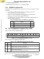
ECHAMR fields are described in Table 7-2.
0 1 2 3 4 5 6 7 8 9 10 11 12 13 14 15
Field MODE0 — OCT SUERM FISU — UN TXB — AERM NID IDL MRF RXF BSY RXB
Reset No reset value
R/W R/W
Offset 0x18
16 17 18 19 20 25 26 27 28 29 31
Field MODE1 POL — IDLM — TS RQN NOF
Reset No reset value 1 No reset value
R/W R/W
Offset 0x1A
Figure 7-1. Extended Channel Mode Register (ECHAMR)
Table 7-2. ECHAMR Fields Description
Bits Name Description
0,16 MODE0
MODE1
00 Transparent mode
01 HDLC mode
10 Reserved
11 SS #7 mode (This is the required bit setting for an MCC to perform SS7.)
1, 5,
8
0 Reserved, must be cleared.
2-4,
6-7,
9-15
INTMSK Interrupt mask bits. Refer to Section 10.1, “Interrupt Table Entry.”
17 POL Enable polling. POL enables the transmitter to poll the TxBDs.
0 Polling is disabled (The CPM does not access the external bus to check the R bit in the TxBD).
1 Polling is enabled.
POL can be used to optimize the use of the external bus. Software should always set POL at the
beginning of a transmit sequence of one or more frames. The CP clears POL when no more
buffers are ready in the transmit queue, i.e. when it finds a BD with R = 0 (for example, at the end
of a frame or at the end of a multi-frame transmission). To prevent a significant number of
useless transactions on the external bus, software should always prepare the new BD, or
multiple BDs, and set BD[R] before enabling polling.
18 1 Reserved, must be set.
Fr
eescale S
emiconduct
or
, I
Freescale Semiconductor, Inc.
For More Information On This Product,
Go to: www.freescale.com
nc...

MOTOROLA
Enhanced SS7 Microcode Specification
9
PRELIMINARY—SUBJECT TO CHANGE WITHOUT NOTICE
Signal Unit Error Monitor (SUERM)
7.2 Signal Unit Error Monitor (
SUERM)
The microcode maintains the signal unit error rate monitor as described in ITU-T Q.703
paragraph 10 and ANSI T1.111-1996 paragraph 10.
The microcode uses SUERM, N, N_cnt, D, D_cnt and T parameters for the leaky-bucket
implementation of the SU error monitor.
• After every N octets received while in octet counting mode, SUERM is incremented
and an interrupt request can be generated (SUERM) depending on the interrupt
mask.
• After D error-free frames have been received, SUERM is decremented. SUERM
will not be decremented below zero.
¥ If SUERM reaches T, the SUERM is cleared and an interrupt is generated.
19 IDLM Idle mode.
0 No idle patterns are transmitted between frames. After transmitting NOF+1 flags, the transmitter
starts sending the data of the frame. If the transmission is between frames and the frame buffers
are not ready, the transmitter sends flags until it can start transmitting the data.
1 At least one idle pattern is sent between adjacent frames. The NOF value shall be no smaller
than the PAD setting, see TxBD. If NOF = 0, this is identical to flag sharing in SS7. Mode flags
precede the actual data. When IDLM = 1, at least one idle pattern is sent between adjacent
frames. If the transmission is between frames and the frame buffer is not ready, the transmitter
sends idle characters. When data is ready, the NOF+1 flags are sent followed by the data frame.
If IDLE mode is selected and NOF = 1, the following sequence is sent:
......init value, FF, FF, flag, flag, data, ........
The init value before the idle will be ones.
For EIM, IDLM must be cleared
20-23 0 Reserved, must be cleared.
24 0 Reserved, must be cleared.
25 0 Reserved, must be cleared.
10 TS Receive time stamp. If this bit is set a 4 byte time stamp is written at the beginning of every data
buffer that the BD points to.If this bit is set the data buffer must start from an address equal to 8*n-4
(n is any integer larger than 0).
11–12 RQN Receive queue number. Specifies the receive interrupt queue number.
00 Queue number 0.
01 Queue number 1.
10 Queue number 2.
11 Queue number 3.
13–15 NOF Number of flags. NOF defines the minimum number of flags before frames:
000 - at least 1 flag
001 - at least 2 flags
....
111 - at least 8 flags
Table 7-2. ECHAMR Fields Description (continued)
Bits Name Description
Fr
eescale S
emiconduct
or
, I
Freescale Semiconductor, Inc.
For More Information On This Product,
Go to: www.freescale.com
nc...

10
Enhanced SS7 Microcode Specification
MOTOROLA
PRELIMINARY—SUBJECT TO CHANGE WITHOUT NOTICE
SS7 Configuration Register (SS7_OPT)
To disable SUERM, refer to Section 7.3.5, “Disabling SUERM.”
7.2.1 SUERM in Japanese SS7
The Japanese SS7 uses a time interval to monitor errors. If an error is present, it checks
every 24 ms.
• An error flag is set that indicates whether current frame is errored or not.
• For every JTRDelay an error flag is checked.
• If there is no error, decrement the counter SUERM by 1 (not below zero).
• If there is an error, increment the counter SUERM by D.
• If SUERM reaches T, the counter SUERM is cleared and a “signal unit error rate
monitor” interrupt is generated.
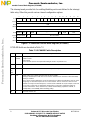
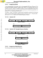
7.3 SS7 Configuration Register (SS7_OPT)
Figure 7-2 shows the SS7 configuration register.
Table 7-4 describes SS7 configuration register fields.
Table 7-3. Parameter Values for SUERM in Japanese SS7
Parameter Definition Value
T Threshold 285
D Upcount 16
JTRDelay Length of interval (24ms) 0x2F
0 1 2 3 4 5 6 7 8 9 10 11 12 15
Field — EN_GB EIM ExtSN AERM SUERM_DIS STD SF_DIS SU_FIL SEN_FIS O_ORN O_ITUT FISU_PAD
Reset No reset value
R/W R/W
Figure 7-2. SS7 Configuration Register (SS7_OPT)
Table 7-4. SS7 Configuration Register Fields Description
Bits Name Description
0 — Reserved, should be cleared.
1 EN_GB Enable GB features in EIM. Refer to Table 7-5 and to Section 7.3.2, “EIM Implementation.”
0 Disable GB features in EIM, only use AnnexA feature.
1 Enable GB features in EIM, EIM and STD must also be set.
2 EIM Errored interval monitor. Refer to Table 7-5 and to Section 7.3.2, “EIM Implementation.”
0 Disable Errored Interval Monitoring.
1 Enable Errored Interval Monitoring, STD must also be set.
Fr
eescale S
emiconduct
or
, I
Freescale Semiconductor, Inc.
For More Information On This Product,
Go to: www.freescale.com
nc...

MOTOROLA Enhanced SS7 Microcode Specification 11
PRELIMINARY—SUBJECT TO CHANGE WITHOUT NOTICE
SS7 Configuration Register (SS7_OPT)
7.3.1 Mode Configurations
Table 7-5 shows the SS7_OPT bit values required for various error monitoring modes.
3 ExtSN EXTended Sequence Number. Refer to Section 7.3.3, “ExtSN Implementation.”
0 Disable Extended Sequence Number.
1 Enable Extended Sequence Number.
4 AERM Alignment error rate monitor enable. Refer to Table 7-5 and to Section 7.3.4, “AERM
Implementation.”
0 Do not enable AERM.
1 Enable AERM.
5 SUERM_
DIS
Disable the error monitoring. Refer to Section 7.3.5, “Disabling SUERM.”
Disable the Japanese SUERM. Refer to Section 7.3.4, “AERM Implementation.”
Disable the errored interval monitor. Refer to Section 7.3.4, “AERM Implementation.”
0 Enable SUERM/Japanese SUERM/EIM.
1 Disable SUERM/Japanese SUERM/EIM.
6 STD Standard compliance. Refer to Table 7-5 and to Section 7.3.6, “STD.”
0 ITU-T/ANSI compliant
1 Japanese SS7 compliant/ITU-T Annex A/GB (EIM)
7 SF_DIS Discard short frames (less than 5 octets or 8 octets if Extended sequence number is enabled)
0 Do not discard short frames.
1 Discard short frames.
8 SU_FIL SU Filtering. Refer to Section 7.3.7, “SU Filtering.”
0 Disable SU filtering.
1 Enable SU filtering.
9 SEN_FIS Send FISU if first BD of frame is not ready.
0 Flags are sent if the current BD, which is the first BD of the frame, does not have its ready bit set.
1 FISUs are automatically sent if the current BD, which is the first BD of the frame, does not have
its ready bit set.
10 O_ORN In ITU-T mode, Enter octet counting mode (OCM) on overrun. Refer to Table 7-6 and to
Section 7.3.8, “Octet Counting Mode.”
0 Disable entering OCM if there are no receive BDs available.
1 Enter OCM if there are no receive BDs available,
In AnnexA/GB/Japanese mode, error counter may increase for current interval on overrun. Refer to
Table 7-6 and to Section 7.3.8, “Octet Counting Mode.”
0 Error counter will not increase if there are no receive BDs available.
1 Error counter will increase if there are no receive BDs available.
11 O_ITUT Enter octet counting mode (OCM) on ITU-T conditions (after an abort sequence or when an SU is
too long). Should be cleared if using the Japanese standard or Annex A/GB (EIM). Refer to
Table 7-6 and to Section 7.3.8, “Octet Counting Mode.”
0 Disable entering OCM on ITU-T conditions.
1 Enable entering OCM on ITU-T conditions.
12-15 FISU_PAD Padding of the automatically transmitted FISUs. If the SEN_FISU bit is set, the CP will use the value
of FISU_PAD as a number of pad character. Please refer to PAD parameter in 7.7.2, “SS7 Transmit
Buffer Descriptor (TxBD).
Table 7-4. SS7 Configuration Register Fields Description (continued)
Bits Name Description
Fr
eescale S
emiconduct
or
, I
Freescale Semiconductor, Inc.
For More Information On This Product,
Go to: www.freescale.com
nc...

12 Enhanced SS7 Microcode Specification MOTOROLA
PRELIMINARY—SUBJECT TO CHANGE WITHOUT NOTICE
SS7 Configuration Register (SS7_OPT)
Table 7-6 shows the SS7_OPT bit values required for Octet count mode.
7.3.2 EIM Implementation
Errored interval monitor (EIM) is implemented instead of SUERM.
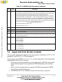
Table 7-5. Error Monitor Modes
Modes EN_GB EIM AERM STD
SUERM. SUERM is the default mode when using ITU-T Q.703. Refer to
Section 7.2, “Signal Unit Error Monitor (SUERM).”
0000
SUERM & AERM in Japanese mode. When STD is set the Japanese mode is
entered and another type of SUERM is used (refer to Section 7.2.1, “SUERM in
Japanese SS7”). Japanese AERM is requires different parameter settings. Refer
to Section 7.3.4.2, “Japanese SS7.”
0001
AERM. See 7.3.1.2, “AERM Implementation. There are no changes for AERM
implementation between standard SS7 and enhanced SS7 except that octet
count mode is not used. Refer to Section 7.3.4, “AERM Implementation.”
0010
Reserved 0011
Reserved 0100
EIM in AnnexA. Refer to the document ITU-T Q.703 (07/96) for Annex A. Also
refer to Section 7.3.2, “EIM Implementation.”
0101
EIM in GB. Refer to the document Chinese National No.7 Signaling System
2Mbit/s High Speed Link Technical Specification. Also refer to Section 7.3.2, “EIM
Implementation.”
1101
Reserved 0/1 1 1 0
Reserved 0/1 1 1 1
Table 7-6. Octet Count Mode
Modes Description O_ORN O_ITUT
SS7 Octet count mode is not used. 0 0
Octet count mode is entered when ABORT is received or SU is too long. 0 1
Octet count mode is entered when no Rx buffers are available. 1 0
Octet count mode is entered when ABORT or SU is too long or when no Rx
buffers are available.
11
Japanese SS7 Error counter does not increase when a Rx buffer is not available 0 0
Error counter does increase when a Rx buffer is not available. 1 0
Enhanced SS7
(Annex A /GB)
Error counter does not increase when a Rx buffer is not available. 0 0
Error counter does increase when a Rx buffer is not available. 1 0
Fr
eescale S
emiconduct
or
, I
Freescale Semiconductor, Inc.
For More Information On This Product,
Go to: www.freescale.com
nc...

MOTOROLA Enhanced SS7 Microcode Specification 13
PRELIMINARY—SUBJECT TO CHANGE WITHOUT NOTICE
SS7 Configuration Register (SS7_OPT)
7.3.2.1 Annex A SS7
As stated in ITU-T Q.703 (07/96) for Annex A, the errored interval monitor is implemented
as follows:
1. On every errored Signal Unit an error flag is set.
2. If the interval is error free; decrement the counter SUERM by 1 (not below zero)
3. If there is an error in the interval; increment the counter SUERM by D.
4. If SUERM reaches T, the counter SUERM is cleared and a “signal unit error rate
monitor” interrupt is generated.
7.3.2.2 GB SS7
According to Chinese National No.7 Signaling System 2Mbit/s High Speed Link Technical
Specification (refer as GB in this manual), EIM is implemented for GB (provided
SS7_OPT[EN_GB] is set) in the following way:
1. On every errored Signal Unit an error flag is set.
2. If the interval is error free, decrement the counter SUERM by U (not below zero).
3. If there is an error in the interval, increment the counter SUERM by D.
4. If SUERM reaches T, the counter SUERM is cleared and a “signal unit error rate
monitor” interrupt is generated.
7.3.3 ExtSN Implementation
The extended sequence number (ExtSN) option implements the ITU-T Q.703 (07/96)
Annex A/GB standard. The option extended sequence number uses 12 instead of 7 bits for
sequence numbering.
Table 7-7. Values for the Annex A Errored Interval Parameters
Parameter Definition 1.5 Mbit/s 2.0 Mbit/s
T Threshold 65 73
D Upcount 16 18
JTRDelay Length of interval (100ms) 0xC3 0xC3
Table 7-8. Values for the GB Errored Interval Parameters
Parameter Definition 2.0 Mbit/ s
T Threshold 794
D Upcount 198
U Downcount 11
JTRDelay Length of interval (100ms) 0xC3
Fr
eescale S
emiconduct
or
, I
Freescale Semiconductor, Inc.
For More Information On This Product,
Go to: www.freescale.com
nc...

14 Enhanced SS7 Microcode Specification MOTOROLA
PRELIMINARY—SUBJECT TO CHANGE WITHOUT NOTICE
SS7 Configuration Register (SS7_OPT)
7.3.4 AERM Implementation
The SS7 microcode implements the ITU Q.703 alignment error rate monitor (AERM). The
microcode uses the T, SUERM, M and M_cnt parameters. The M_cnt parameter is
incremented for every T errored frames. If M_cnt reaches M, an AERM interrupt is
generated to layer 3.
Note that in AERM mode no SUERM interrupt is generated. Also, the algorithm associated
with D and D_cnt is disabled as per the ITU specification.
7.3.4.1 Annex A/GB SS7
The EIM or STD options cannot be set when using ITU Q.703 AERM. Also note that the
octet count mode is not used in Annex A/GB.
To disable AERM and enter EIM, do the following:
1. Set SUERM_DIS bit in SS7_OPT.
2. Clear AERM bit in SS7_OPT.
3. Annex A: set up parameters (T, D, SUERM) for EIM.
GB: set up parameters (T, D, U, SUERM) for EIM.
4. Set EIM and STD bits in SS7_OPT.
5. Clear SUERM_DIS bit in SS7_OPT.
7.3.4.2 Japanese SS7
To meet the Japanese AERM requirements the user must change the parameters T and D.
Note that the interrupt generated is not AERM but SUERM.
During proving, do the following:
1. Set SS7_OPT register to 0b0000 001X XX00 XXXX. The value of X does not
matter because these bits do not affect the operation of the error counter.
2. Clear JTRdelay parameter to'0.'
3. Set parameters T(threshold) and D(up counter) to '1.'
4. Clear parameter SUERM (error counter) to '0.'
5. Set JTTDelay to value required to generate 24ms delay.
These settings allow FISU or LSSU transmission to be delayed by the required 24ms
(JTTDelay). They also allow the correct operation of the JT Q703 error counter and ensure
that an SUERM interrupt is generated on the first SU received in error.
After proving period, set the parameters (T and D) to values according to the Japanese
SUERM. See section Table 7-3.
Fr
eescale S
emiconduct
or
, I
Freescale Semiconductor, Inc.
For More Information On This Product,
Go to: www.freescale.com
nc...

MOTOROLA Enhanced SS7 Microcode Specification 15
PRELIMINARY—SUBJECT TO CHANGE WITHOUT NOTICE
SS7 Configuration Register (SS7_OPT)
To disable AERM and enter SUERM, do the following:
1. Set SUERM_DIS bit in SS7_OPT.
2. Set parameters (T, D & SUERM) for Japanese SUERM.
3. Clear SUERM_DIS bit in SS7_OPT.
7.3.5 Disabling SUERM
When SS7_OPT[SUERM_DIS] is set, the N_cnt and D_cnt parameters are not
decremented by the microcode and no SUERM interrupt is generated. This allows these
parameters to be updated, for example, at the end of the proving period in alignment error
monitoring. If the SS7 controller is in the octet counting mode (OCM), the user software
should wait until an error free frame is received upon which OCM is left, thereby
deactivating the N_cnt parameter. Hence, after setting SUERM_DIS, it is recommended to
wait one good frame length before changing the SUERM counter parameters.
7.3.6 STD
When SS7_OPT[STD] is set and SS7_OPT[EIM] is cleared, the Japanese SS7 mode is
entered. It will use it’s own signal unit error monitoring that checks every 24 ms if an error
is present. The AERM implementation in ITU Q.703 is not applicable on Japanese SS7. It
also differs from the ITU Q.703 standard by sending the AUTOFISU with a 24 ms delay.
Both EIM and Japanese SUERM use a time interval to monitor errors.
7.3.6.1 Annex A SS7
When both SS7_OPT[STD] and SS7_OPT[EIM] are set, the microcode implements the
ITU-T Q.703 (07/96) for Annex A. Annex A uses EIM instead of SUERM.
7.3.6.2 GB SS7
When SS7_OPT[EN_GB], SS7_OPT[STD] and SS7_OPT[EIM] are set, the microcode
implements the GB features. GB uses EIM instead of SUERM.
7.3.7 SU Filtering
To reduce overhead to the user software, a filtering algorithm has been adopted to allow
superfluous frames to be discarded. This algorithm compares the first 3–5 bytes (6-8 if
ExtSN is used) of the current FISU or LSSU to the last SU received and discards the current
SU if it has already been received twice.
Fr
eescale S
emiconduct
or
, I
Freescale Semiconductor, Inc.
For More Information On This Product,
Go to: www.freescale.com
nc...

16 Enhanced SS7 Microcode Specification MOTOROLA
PRELIMINARY—SUBJECT TO CHANGE WITHOUT NOTICE
SS7 Configuration Register (SS7_OPT)
7.3.7.1 Comparison Mask
A user programmable 8-byte mask exists in the parameter RAM map. When an SU is
received, the controller checks the contents of the LI field. If LI is between 0 and 2, the SU
(except for the CRC portion) is masked according to the user programmable mask and is
then compared to the last SU received. The state machine for the matching algorithm is in
Section 7.3.7.2, “Comparison State Machine.”
The Mask 1, Mask 2, and Mask 3 channel-specific parameters construct the 8-byte user
mask. The exact format and byte ordering are shown in Section 7.3.6.1.1, “Mask for SS7,”
and Section 7.3.7.1.2, “Mask for SS7 Extended Sequence Number.”
7.3.7.1.1 Mask for SS7
7.3.7.1.2 Mask for SS7 Extended Sequence Number
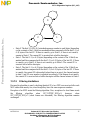
7.3.7.2 Comparison State Machine
The following state machine exists for filtering.
msb lsb
Byte 1 Byte 2 Byte 3 Byte 4
Figure 7-3. Mask 1
msb lsb
Reserved, should be cleared. Byte 5
Figure 7-4. Mask 2
msb lsb
Byte 1 Byte 2 Byte 3 Byte 4
Figure 7-5. Mask 1
msb lsb
Byte 5 Byte 6
Figure 7-6. Mask 2
msb lsb
Byte 7 Byte 8
Figure 7-7. Mask 3
Fr
eescale S
emiconduct
or
, I
Freescale Semiconductor, Inc.
For More Information On This Product,
Go to: www.freescale.com
nc...

MOTOROLA Enhanced SS7 Microcode Specification 17
PRELIMINARY—SUBJECT TO CHANGE WITHOUT NOTICE
SS7 Configuration Register (SS7_OPT)
• State 0. The first 3–5 (or 6–8 if extended sequence number is used) bytes (depending
on the contents of the LI field) are masked and then compared with the first 3–5 (or
6–8) bytes of the last SU. If there is a match, go to State 1; if there is not a match,
remain in State 0. The current SU is received into a buffer descriptor.
• State 1. The first 3–5 (or 6–8) bytes (depending on the content of the LI field) are
masked and then compared with the first 3–5 (or 6–8) bytes of the last SU. If there
is a match, go to State 2; if there is not a match, go to State 0. The current SU is
received into a buffer descriptor.
• State 2. The first 3–5 (or 6–8) bytes (depending on the content of the LI field) are
masked and then compared with the first 3–5 (or 6–8) bytes of the last SU. If there
is a match, the current SU is discarded (unless there is an error), the channel remains
in state 2, and SU error monitor is adjusted accordingly. If the frames do not match,
the current SU is received into a buffer descriptor and the channel returns to State 0.
7.3.7.3 Filtering Limitations
Because the algorithm is purely checking identical SUs, two FISUs are received after each
MSU rather than merely one, even though they have the same sequence numbers.
Reception of an MSU resets the filtering algorithm. Also, reception of a short frame resets
the filtering algorithm when SS7_OPT[SF_DIS] = 0; however, when
SS7_OPT[SF_DIS] = 1 (short frames are discarded), the filtering algorithm remains
unchanged.
1
0
2
Fr
eescale S
emiconduct
or
, I
Freescale Semiconductor, Inc.
For More Information On This Product,
Go to: www.freescale.com
nc...

18 Enhanced SS7 Microcode Specification MOTOROLA
PRELIMINARY—SUBJECT TO CHANGE WITHOUT NOTICE
SS7 Configuration Register (SS7_OPT)
7.3.7.4 Resetting the SU Filtering Mechanism
This command resets the filtering algorithm to ensure that the next SU is received, even if
it would normally have been filtered. This command could be issued periodically so that the
603e core can check to make sure that the link is up and not simply receiving flags.
To issue this MCC command, refer to Section 13.4, “Command Set,” in the MPC8260
PowerQUICC II User’s Manual. Use opcode 1110 (0xE).
7.3.8 Octet Counting Mode
When entering the octet counting mode (OCM), the CP loads the user defined N register to
its internal octet counter. While in the octet counting mode the CP decrements its internal
counter for every unstuffed octet received. When the internal counter is decremented to
zero, the CP increment the SUERM register and reload the N register into the internal count
register. In addition, an interrupt (OCT) might be generated depending on the interrupt
mask. The SS7 controller enters octet counting mode under the following circumstances:
• An ABORT character is received at any time and SS7_OPT[O_ITUT] is set.
• The SU currently being received has exceeded the length programmed in the MFLR
register and SS7_OPT[O_ITUT] is set.
• The receiver overruns and SS7_OPT[O_ORN] is set. Note that when no receive
buffers are available, only octets are counted (that is, D_cnt is not decremented after
receiving the frame).
The SS7 controller leaves octet counting mode when a valid signal unit is detected (with a
valid CRC and a length less than MFLR and greater than 4).
NOTE
Octet counting mode applies only to the ITU-T and ANSI
standards. The SS7 microcode does not work if both the
Japanese standard or Annex A/GB (EIM) and OCM features
are selected. Refer to Table 7-6.
Part VIII TDM Mapping
The mapping of SS7 channels to TDM channels is identical to mapping of MCC channels.
Refer to Section 27.8, “MCC Configuration Register,” in the MPC8260 PowerQUICC II
User’s Manual.
Fr
eescale S
emiconduct
or
, I
Freescale Semiconductor, Inc.
For More Information On This Product,
Go to: www.freescale.com
nc...
Page is loading ...
Page is loading ...
Page is loading ...
Page is loading ...
Page is loading ...
Page is loading ...
Page is loading ...
Page is loading ...
-
 1
1
-
 2
2
-
 3
3
-
 4
4
-
 5
5
-
 6
6
-
 7
7
-
 8
8
-
 9
9
-
 10
10
-
 11
11
-
 12
12
-
 13
13
-
 14
14
-
 15
15
-
 16
16
-
 17
17
-
 18
18
-
 19
19
-
 20
20
-
 21
21
-
 22
22
-
 23
23
-
 24
24
-
 25
25
-
 26
26
-
 27
27
-
 28
28


Ask a question and I''ll find the answer in the document
Finding information in a document is now easier with AI
Related papers
Other documents
-
Freescale Semiconductor MPC8265 User manual
-
Motorola DigitalDNA MPC180E User manual
-
-
 T'nB CSUBOMB2 Datasheet
-
 T'nB CSPUREWH Datasheet
-
Cisco Systems Doll VR-561 User manual
-
Dialogic NaturalAccess™ MTP2 Layer Developer's Reference Manual
-
-
-
 SkylinkHome LS-318 User manual


