Samsung SPINPOINT V40 Series User manual
- Category
- Internal hard drives
- Type
- User manual

Product Manual
3.5” Hard Disk Drives
SPINPOINT V40
JULY 7, 2001 (Rev 1.0)

ii SpinPoint V40 Product Manual

SpinPoint V40 Product Manual
iii
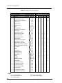
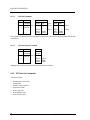
TABLE OF CONTENTS
CHAPTER 1 SCOPE..................................................................................................................................1
1.1 U
SER DEFINITION ............................................................................................................................... 1
1.2 M
ANUAL ORGANIZATION ...................................................................................................................1
1.3 T
ERMINOLOGY AND CONVENTIONS....................................................................................................2
1.4 R
EFERENCE......................................................................................................................................... 3
CHAPTER 2 DESCRIPTION....................................................................................................................4
2.1 I
NTRODUCTION...................................................................................................................................4
2.2 K
EY FEATURES................................................................................................................................... 4
2.3 S
TANDARDS AND REGULATIONS......................................................................................................... 5
2.4 H
ARDWARE REQUIREMENTS ..............................................................................................................5
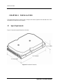
CHAPTER 3 SPECIFICATIONS.............................................................................................................. 6
3.1 S
PECIFICATION SUMMARY.................................................................................................................. 6
3.2 P
HYSICAL SPECIFICATIONS................................................................................................................. 7
3.3 L
OGICAL CONFIGURATIONS................................................................................................................ 7
3.4 P
ERFORMANCE SPECIFICATIONS......................................................................................................... 8
3.5 P
OWER REQUIREMENTS...................................................................................................................... 9
3.6 E
NVIRONMENTAL SPECIFICATIONS................................................................................................... 10
3.7 R
ELIABILITY SPECIFICATIONS .......................................................................................................... 11
CHAPTER 4 INSTALLATION...............................................................................................................12
4.1 S
PACE REQUIREMENTS.....................................................................................................................12
4.2 U
NPACKING INSTRUCTIONS..............................................................................................................13
4.3 M
OUNTING ....................................................................................................................................... 13
4.3.1 Orientation............................................................................................................................... 13
4.3.2 Clearance ................................................................................................................................. 15
4.3.3 Ventilation ...............................................................................................................................16
4.4 C
ABLE CONNECTORS........................................................................................................................16
4.4.1 DC Power Connector............................................................................................................... 16
4.4.2 AT-Bus Interface Connector....................................................................................................16
4.5 J
UMPER BLOCK CONFIGURATIONS.................................................................................................... 18
4.6 D
RIVE INSTALLATION....................................................................................................................... 20
4.7 S
YSTEM STARTUP PROCEDURE......................................................................................................... 21
4.7.1 Drive Installation to Access the Full Capacity Using 32GB Clip............................................ 22
CHAPTER 5 DISK DRIVE OPERATION............................................................................................. 23
5.1 H
EAD / DISK ASSEMBLY (HDA).......................................................................................................23
5.1.1 Base Casting Assembly............................................................................................................ 23
5.1.2 DC Spindle Motor Assembly................................................................................................... 23
5.1.3 Disk Stack Assembly...............................................................................................................25
5.1.4 Head Stack Assembly .............................................................................................................. 25
5.1.5 Voice Coil Motor and Actuator Latch Assemblies.................................................................. 25
5.1.6 Air Filtration System................................................................................................................25
5.2 D
RIVE ELECTRONICS ........................................................................................................................ 26
5.2.1 Digital Signal Process and Interface Controller....................................................................... 26
5.2.2 AT Disk Controller .................................................................................................................. 26
5.2.2.1 The Host Interface Control Block........................................................................................................28
5.2.2.2 The Buffer Control Block ....................................................................................................................29
5.2.2.3 The Disk Control Block.......................................................................................................................29
5.2.2.4 The Disk ECC Control Block...............................................................................................................31
5.2.2.5 Frequency Synthesizer.........................................................................................................................31
5.2.2.6 Power Management..............................................................................................................................31
5.2.3 Read/Write IC.......................................................................................................................... 31

iv SpinPoint V40 Product Manual
5.2.3.1 Time Base Generator........................................................................................................................... 32
5.2.3.2 Automatic Gain Control...................................................................................................................... 32
5.2.3.3 Asymmetry Correction Circuitry (ASC).............................................................................................. 32
5.2.3.4 Analog Anti-Aliasing Low Pass Filter................................................................................................. 32
5.2.3.5 Analog to Digital Converter (ADC) and FIR ...................................................................................... 32
5.3 SERVO SYSTEM.................................................................................................................................34
5.4 R
EAD AND WRITE OPERATIONS........................................................................................................34
5.4.1 The Read Channel....................................................................................................................34
5.4.2 The Write Channel...................................................................................................................35
5.5 F
IRMWARE FEATURES.......................................................................................................................35
5.5.1 Read Caching...........................................................................................................................35
5.5.2 Write Caching ..........................................................................................................................36
5.5.3 Defect Management .................................................................................................................37
5.5.4 Automatic Defect Allocation ...................................................................................................37
5.5.5 Multi-burst ECC Correction.....................................................................................................37
5.5.6 SMART....................................................................................................................................37
5.5.7 AAM…………………………………………………………………………………………..37
CHAPTER 6 AT INTERFACE AND ATA COMMANDS....................................................................39
6.1 I
NTRODUCTION .................................................................................................................................39
6.2 P
HYSICAL INTERFACE.......................................................................................................................39
6.2.1 Signal Conventions ..................................................................................................................39
6.2.2 Signal Summary.......................................................................................................................39
6.2.3 Signal Descriptions ..................................................................................................................40
6.2.3.1 CS1FX- (Drive Chip Select 0)............................................................................................................. 40
6.2.3.2 CS3FX- (Drive Chip Select 1)............................................................................................................. 40
6.2.3.3 DA0-2 (Drive Address Bus)................................................................................................................ 40
6.2.3.4 DASP- (Drive Active/Slave Present)................................................................................................... 40
6.2.3.5 DD0-DD15 (Drive Data Bus).............................................................................................................. 40
6.2.3.6 DIOR- (Drive I/O Read)...................................................................................................................... 40
6.2.3.7 DIOW- (Drive I/O Write).................................................................................................................... 40
6.2.3.8 DMACK- (DMA Acknowledge)......................................................................................................... 41
6.2.3.9 DMARQ (DMA Request) ................................................................................................................... 41
6.2.3.10 INTRQ (Drive Interrupt)................................................................................................................. 41
6.2.3.11 IOCS16- (Drive 16-bit I/O)............................................................................................................. 41
6.2.3.12 IORDY (I/O Channel Ready).......................................................................................................... 42
6.2.3.13 PDIAG- (Passed Diagnostics)......................................................................................................... 42
6.2.3.14 RESET- (Drive Reset)..................................................................................................................... 42
6.3 LOGICAL INTERFACE.........................................................................................................................46
6.3.1 General.....................................................................................................................................46
6.3.1.1 Bit Conventions................................................................................................................................... 46
6.3.1.2 Environment........................................................................................................................................ 46
6.3.2 I/O Register - Address..............................................................................................................48
6.3.3 Control Block Register Descriptions........................................................................................49
6.3.3.1 Alternate Status Register (3F6h) ......................................................................................................... 49
6.3.3.2 Drive Address Register (3F7h)............................................................................................................ 49
6.3.3.3 Device Control Register (3F6h)........................................................................................................... 49
6.3.4 Command Block Register Descriptions...................................................................................50
6.3.4.1 Data Register (1F0h) ........................................................................................................................... 50
6.3.4.2 Features Register (1F1h) ..................................................................................................................... 50
6.3.4.3 Sector Number Register (1F3h)........................................................................................................... 50
6.3.4.4 Error Register (1F1h) .......................................................................................................................... 50
6.3.4.5 Sector Count Register (1F2h).............................................................................................................. 51
6.3.4.6 Cylinder High Register (1F5h)............................................................................................................ 51
6.3.4.7 Cylinder Low Register (1F4h)............................................................................................................. 51
6.3.4.8 Command Register (1F7h).................................................................................................................. 51
6.3.4.9 Drive/Head Register (1F6h)................................................................................................................ 51
6.3.4.10 Status Register (1F7h)..................................................................................................................... 52
6.4 AT COMMAND REGISTER DESCRIPTIONS ..........................................................................................53
6.4.1 Check Power Mode (98h, E5h)................................................................................................56
6.4.2 Download Micro Code (92h) ...................................................................................................56
6.4.3 Execute Device Diagnostics (90h)...........................................................................................56

SpinPoint V40 Product Manual
v
6.4.4 Flush Cache (E7h).................................................................................................................... 57
6.4.5 Format Track (50h).................................................................................................................. 57
6.4.6 Identify Device (ECh)..............................................................................................................57
6.4.7 Idle (97h,E3h)..........................................................................................................................62
6.4.8 Idle Immediate (95h,E1h)........................................................................................................62
6.4.9 Initialize Device Parameters (91h)........................................................................................... 62
6.4.10 Read Buffer (E4h)....................................................................................................................63
6.4.11 Read DMA (C8h:with retry, C9h:without retry)..................................................................... 63
6.4.12 Read Long (22h:with retry, 23h: without retry)...................................................................... 63
6.4.13 Read Multiple Command (C4h)...............................................................................................64
6.4.14 Read Native Max Address (F8h)..............................................................................................65
6.4.15 Read Sector(s) (20h:with retry, 21h:without retry)................................................................. 65
6.4.16 Read Verify Sector(s) (40h:with retry, 41h:without retry)...................................................... 66
6.4.17 Recalibrate (1xh)......................................................................................................................66
6.4.18 Seek (7xh)................................................................................................................................ 66
6.4.19 Set Features (EFh).................................................................................................................... 67
6.4.20 Set Max Address (F9h)............................................................................................................ 69
6.4.21 Set Multiple Mode (C6h)......................................................................................................... 70
6.4.22 Sleep (99h, E6h).......................................................................................................................70
6.4.23 Standby (96h,E2h) ................................................................................................................... 71
6.4.24 SMART (B0h) ......................................................................................................................... 71
6.4.24.1 Smart disable operation (D9h).........................................................................................................71
6.4.24.2 Smart enable/disable attribute autosave (D2h) ................................................................................72
6.4.24.3 Smart enable operations (D8h)........................................................................................................72
6.4.24.4 Smart execute off-line immediate (D4h) .........................................................................................72
6.4.24.5 Smart read data (D0h)......................................................................................................................73
6.4.24.6 SMART read log sector (D5h).........................................................................................................75
6.4.24.7 SMART return status (DAh)............................................................................................................75
6.4.24.8 SMART save attribution value (D3h)..............................................................................................75
6.4.24.9 SMART write log sector (D6h).......................................................................................................75
6.4.25 Standby (96h, E2h) ..................................................................................................................76
6.4.26 Standby Immediate (94h, E0h) ................................................................................................76
6.4.27 Write Buffer (E8h)...................................................................................................................76
6.4.28 Write Long (32h:with retry, 33h:without retry)...................................................................... 76
6.4.29 Write DMA (CAh)................................................................................................................... 76
6.4.30 Write Multiple Command (C5h)..............................................................................................77
6.4.31 Write Sector(s) (30h:with retry, 31h:without retry).................................................................77
6.5 P
ROGRAMMING REQUIREMENTS....................................................................................................... 79
6.5.1 Reset Response ........................................................................................................................ 79
6.5.2 Error Posting............................................................................................................................ 79
6.5.3 Power Conditions.....................................................................................................................81
6.5.3.1 Sleep mode...........................................................................................................................................81
6.5.3.2 Standby mode.......................................................................................................................................81
6.5.3.3 Idle mode .............................................................................................................................................81
6.5.3.4 Normal mode .......................................................................................................................................82
6.6 PROTOCOL OVERVIEW...................................................................................................................... 83
6.6.1 PIO Data in Commands........................................................................................................... 83
6.6.1.1 PIO Read Command ............................................................................................................................84
6.6.1.2 PIO Read Aborted Command ..............................................................................................................84
6.6.2 PIO Data Out Commands ........................................................................................................ 84
6.6.2.1 PIO Write Command ...........................................................................................................................85
6.6.2.2 PIO Write Aborted Command..............................................................................................................85
6.6.3 Non-Data Commands............................................................................................................... 86
6.6.4 DMA Data Transfer Commands..............................................................................................87
6.6.4.1 Normal DMA transfer..........................................................................................................................88
6.6.4.2 Aborted DMA transfer.........................................................................................................................88
6.6.4.3 Aborted DMA Command.....................................................................................................................88
6.7 TIMING .............................................................................................................................................89
6.7.1 Register transfers ..................................................................................................................... 89
6.7.2 PIO data transfers..................................................................................................................... 91
6.7.3 Multiword DMA data transfer ................................................................................................. 94

vi SpinPoint V40 Product Manual
6.7.4 Ultra DMA data transfer ..........................................................................................................96
6.7.4.1 Initiating an Ultra DMA data in burst.................................................................................................. 96
6.7.4.2 Ultra DMA data burst timing requirements......................................................................................... 97
6.7.4.3 Sustained Ultra DMA data in burst......................................................................................................98
6.7.4.4 Host pausing an Ultra DMA data in burst ........................................................................................... 99
6.7.4.5 Device terminating an Ultra DMA data in burst................................................................................ 100
6.7.4.6 Host terminating an Ultra DMA data in burst....................................................................................101
6.7.4.7 Initiating an Ultra DMA data out burst.............................................................................................. 102
6.7.4.8 Sustained Ultra DMA data out burst.................................................................................................. 103
6.7.4.9 Device pausing an Ultra DMA data out burst.................................................................................... 104
6.7.4.10 Host terminating an Ultra DMA data out burst............................................................................. 105
6.7.4.11 Device terminating an Ultra DMA data out burst ......................................................................... 106
CHAPTER 7 MAINTENANCE.............................................................................................................107
7.1 G
ENERAL INFORMATION.................................................................................................................107
7.2 M
AINTENANCE PRECAUTIONS ........................................................................................................107
7.3 S
ERVICE AND REPAIR.....................................................................................................................107
TABLE OF TABLES
Table 3-1 Specifications............................................................................................................................6
Table 3-2 Physical Specifications..............................................................................................................7
Table 3-3 Logical Configurations..............................................................................................................7
Table 3-4 Performance Specifications.......................................................................................................8
Table 3-5 Power Requirements .................................................................................................................9
Table 3-6 Environmental Specifications..................................................................................................10
Table 3-6 Environmental Specifications (continued)..............................................................................11
Table 3-7 Reliability Specifications ........................................................................................................11
Table 4-1 Power Connector Pin Assignment...........................................................................................16
Table 4-2 Logical Drive Parameters........................................................................................................21
Table 6-1 AT-Bus Interface Signals........................................................................................................43
Table 6-2 Interface Signals Description ..................................................................................................45
Table 6-3 I/O Port Function/Selection Address.......................................................................................48
Table 6-4 Command Codes and Parameters............................................................................................54
Table 6-5 Diagnostic Codes ....................................................................................................................57
Table 6-6 IDENTIFY DEVICE information...........................................................................................58
Table 6-7 Automatic Standby Timer Periods..........................................................................................62
Table 6-8 Set Feature Register Definitions..............................................................................................67
Table 6-9 Transfer mode values..............................................................................................................67
Table 6-10 SMART Feature register values............................................................................................71
Table 6-11 Device SMART data structure..............................................................................................73
Table 6-12 Off-line data collection status values ....................................................................................74
Table 6-13 Command Errors...................................................................................................................80
Table 6-14 Power Saving Mode..............................................................................................................81
Table 6-15 Power Conditions..................................................................................................................82
Table 6-16 Register transfer to/from device............................................................................................91
Table 6-17 PIO data transfer to/from device ...........................................................................................93
Table 6-18 Multiword DMA data transfer...............................................................................................95
Table 6-19 Ultra DMA data burst timing requirements...........................................................................97

SpinPoint V40 Product Manual
vii
TABLE OF FIGURES
Figure 4-1 Mechanical Dimension..........................................................................................................12
Figure 4-2 Mounting Dimensions (in Millimeters) .................................................................................14
Figure 4-3 Mounting-Screw Clearance ...................................................................................................15
Figure 4-4
DC Power Connector, Configuration Jumper Block & AT-Bus Interface Connector (JHST)......17
Figure 4-5 Jumper Pin Locations on the Drive PCBA............................................................................19
Figure 4-6 Options for Jumper Block Configuration ..............................................................................19
Figure 4-7 DC Power Connector and AT-Bus Interface Cable Connections.......................................... 20
Figure 5-1 Exploded Mechanical View................................................................................................... 24
Figure 5-2 SID2001 AT Controller Block Diagram................................................................................27
Figure 5-3 Read/Write 88C5200............................................................................................................. 33
Figure 6-1 Register transfer to/from device ............................................................................................90
Figure 6-2 PIO data transfer to/from device............................................................................................92
Figure 6-3 Multiword DMA data transfer............................................................................................... 94
Figure 6-4 Initiating an Ultra DMA data in burst.................................................................................... 96
Figure 6-5 Sustained Ultra DMA data in burst........................................................................................ 98
Figure 6-6 Host pausing an Ultra DMA data in burst .............................................................................99
Figure 6-7 Device terminating an Ultra DMA data in burst.................................................................. 100
Figure 6-8 Host terminating an Ultra DMA data in burst .....................................................................101
Figure 6-9 Initiating an Ultra DMA data out burst................................................................................ 102
Figure 6-10 Sustained Ultra DMA data out burst..................................................................................103
Figure 6-11 Device pausing an Ultra DMA data out burst.................................................................... 104
Figure 6-12 Host terminating an Ultra DMA data out burst..................................................................105
Figure 6-13 Device terminating an Ultra DMA data out burst……………….…………...…………...106


SCOPE
SpinPoint V40 Product Manual
1
CHAPTER 1 SCOPE
Welcome to the SpinPoint V40 series of Samsung hard disk drives. This series of drives consists of the
following models: SV2001H, SV3012H,SV4002H, SV6003H,SV6014H and SV8004H. This chapter
provides an overview of the contents of this manual, including the intended user, manual organization,
terminology and conventions. In addition, it provides a list of references that might be helpful to the reader.
1.1 User Definition
The SpinPoint V40 product manual is intended for the following readers:
• Original Equipment Manufacturers (OEMs)
• Distributors
1.2 Manual Organization
This manual provides information about installation, principles of operation, and interface command
implementation. It is organized into the following chapters:
• Chapter 1 - SCOPE
• Chapter 2 - DESCRIPTION
• Chapter 3 - SPECIFICATIONS
• Chapter 4 - INSTALLATION
• Chapter 5 - DISK DRIVE OPERATION
• Chapter 6 - AT INTERFACE and ATA COMMANDS
• Chapter 7 - MAINTENANCE
In addition, this manual contains a glossary of terms to help you understand important information.

SCOPE
SpinPoint V40
Product Manual
2
1.3 Terminology and Conventions
The following abbreviations are used in this manual:
µinches Microinches(10
-6
inches)
µs Microseconds
Bpi Bits per inch
DB Decibels
Fci Flux changes per inch
GB Gigabytes
Hz Hertz
Kbytes Kilobytes
Lb Pounds
M Meter
MA Milliampere
MB Megabytes
Mbit/s Megabits per second
Mbytes/s Megabytes per second
MHz Megahertz
Mil Millinches
Ms Milliseconds
MV Millivolts
Ns Nanoseconds
Rpm Rotations per minute
Tpi Tracks per inch
V Volts
W Watts
This manual uses the following conventions:
• Computer Message
Computer message refers to items you type at the computer keyboard. These items are listed in all
capitals in Courier New font. For example:
FORMAT C:/S
• Commands and Messages
Interface commands and messages sent from the drive to the host are listed in all capitals. For example:
READ SECTORS
WRITE LONG

SCOPE
SpinPoint V40 Product Manual
3
• Parameters
Parameters are given as initial capitals when spelled out and as all capitals when abbreviated. For
example:
Prefetch Enable: PE
Cache Enable: CE
• Names of Bits and Registers
Bit names and register names are presented in initial capitals. For example:
Host Software Reset
Sector Count Register
• Hexadecimal Notation
Hexadecimal notation is identified using the small letterform. For example:
30h
• Signal Negation
An active low signal name is listed with a dash character (-) following the signal name. For example:
IOR-
• Notes
Notes are used after tables to provide you with supplementary information.
• Host
In general, the system in which the drive resides is referred to as the host.
1.4 Reference
For additional information about the AT interface, refer to:
• ATA-2 (AT Attachment 2), Revision 3, January, 1995
• ATA-3 (Attachment-3 Interface) Revision 7b, 27 January, 1997
• ATA-4 (AT Attachment with Packet Interface Extension) Revision 18, 19 august 1998
• ATA-5 (AT Attachment with Packet Interface Extension) Revision 3, 29 February 2000
• ATA-6 (AT Attachment with Packet Interface Extension)

DESCRIPTION
SpinPoint V40
Product Manual
4
CHAPTER 2 DESCRIPTION
This chapter summarizes general functions and key features of the Spinpoint V40 drive, as well as the
standards and regulations they meet.
2.1 Introduction
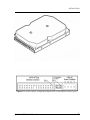
The Samsung SpinPoint V40 3.5 inch disk drives are high capacity, high performance random access storage
devices, which use non-removable 3.5-inch disks as storage media. Each disk incorporates thin film metallic
media technology for enhanced performance and reliability. And for each disk surface there is a
corresponding movable head actuator assembly to randomly access the data tracks and write or read the user
data. The formatted capacities of the SpinPoint V40 family are 20.0,30.06,40.0,60.0,60.06 and 80.0 gigabytes
of storage. Samsung defines a gigabyte (GB) as one billion bytes.
The SpinPoint V40 drives include the AT controller embedded in the disk drive PCB electronics. The drive's
electrical interface is compatible with all mandatory, optional and vendor-specific commands within the ATA
specification.
Drive size conforms to the industry standard 3.5-inch form factor. The interface connectors are the standard
40-pin for AT Interface and 4-pin for DC power supplies.
The SpinPoint V40 incorporates Advanced GMR (Giant Magneto Resistive) head and Noise Predictive
PRML (Partial Response Maximum Likelihood) signal processing technologies. These advanced
technologies allow for an areal density of over 29.18 gigabits per square inch and storage capacity of over
40.06 gigabytes per disk.
The heads, disk(s), and actuator housing are environmentally sealed within an aluminum-alloy base and
cover. As the disks spin, air circulates within this base and cover, commonly referred to as the head and disk
assembly (HDA), through a non-replaceable absolute filter ensuring a contamination free environment for the
heads and disks throughout the life of the drive.
2.2 Key Features
Key features of the SpinPoint V40 hard disk drives include:
• Formatted capacities are 20.0,30.06, 40.0, 60.0,60.06 and 80.0 Gbytes
• Low-profile, 1-inch height form factor
• 8.9 msec average seek time
• High accuracy rotary voice coil actuator with embedded sector servo
• Ultra ATA33/66/100 interface
• ATA standard PIO Mode 4/DMA Mode 2/Ultra DMA Mode 4 & 5(UDMA 66/100) support
• Supports both CHS and LBA Addressing modes
• Supports all logical geometries as programmed by the host

DESCRIPTION
SpinPoint V40 Product Manual
5
• Proprietary 2048KB read look-ahead cache with a segmented buffer and write stacking capability
• Transparent media defect mapping
• Read and write mode auto-reassign
• High performance in-line defective sector skipping
• Automatic error correction and retries
• Optimized 480-bit ECC and 7-byte CRC with 10 way interleave on-the-fly (OTF) correction
• Automatic magnet latch
• Noise predictive PRML read channel
• 2
nd
generation TA detection and correction
• Dynamic anti-stiction algorithm
• Advanced GMR head
• SMART support
• Cable select ability
• Supported Automatic Acoustic Management (AAM)
2.3 Standards and Regulations
The SpinPoint V40 depends upon its host equipment to provide power and appropriate environmental
conditions to achieve optimum performance and compliance with applicable industry and governmental
regulations. Special attention has been given in the areas of safety, power distribution, shielding, audible
noise control, and temperature regulation.
The SpinPoint V40 hard disk drives satisfy the following standards and regulations:
• Underwriters Laboratory (UL): Standard 1950. Information technology equipment including business
equipment.
• Canadian Standards Association (CSA): Standard C22.2 No.3000-201 Information technology
equipment including business equipment.
• Technisher Überwachungs Verein (TUV): Standard EN 60 950. Information technology equipment
including business equipment.
2.4 Hardware Requirements
SpinPoint V40 hard disk drives are designed for use with host computers and controllers that are PC/AT
compatible. They are connected to a PC either by:
• Using an adapter board, or
• Plugging a cable from the drive directly into a PC motherboard with an IDE (Integrated Drive
Electronics) interface.

SPECIFICATIONS
SpinPoint V40
Product Manual
6
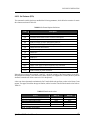
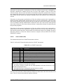
CHAPTER 3 SPECIFICATIONS
This chapter gives a detailed description of the physical, electrical, and environmental characteristics of the
SpinPoint V40 hard disk drives.
3.1 Specification Summary
Table 3-1 Specifications
DESCRIPTION SV2001H SV3012H SV4002H SV6003H SV6014H SV8004H
Number of Disks 1 1 1 2 2 2
Number of R/W heads 1 2 2 3 4 4
Maximum recording density (bpi) 504K
Maximum flux density (fci) 536K
Track density (tpi) 57,500/55,000/52,000
Data tracks per surface (maximum) 55,850
Encoding method Noise Predictive PRML
Interface Ultra ATA / 66/100
Actuator type Rotary Voice Coil
Servo type Embedded Sector Servo
Number of Cylinder Reserved 8
Maximum Writing Frequency (MHz)
235.56
Spindle speed (rpm)
5,400 ± 0.35%

SPECIFICATIONS
SpinPoint V40 Product Manual
7
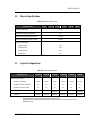
3.2 Physical Specifications
Table 3-2 Physical Specifications
DESCRIPTION SV2001H SV3012H SV4002H SV6003H SV6014H SV8004H
Track pitch (µinches) 17.39
Data head flying height (µinches) 0.5
Inner most data track radius (inches) 0.8204
Outer most data track radius (inches) 1.8031
Physical dimensions:
Length (inches)
Width (inches)
Height (inches)
Weight (lb)
5.75
4.00
1.00
1.4
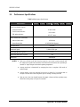
3.3 Logical Configurations
Table 3-3 Logical Configurations
DESCRIPTION SV2001H SV3012H SV4002H SV6003H SV6014H SV8004H
Default logical mode:
Number of cylinders
Number of heads / cylinders
Number of sectors / heads
38,869
16
63
58,246
16
63
77,622
16
63
116,374
16
63
116,375
16
63
155,127
16
63
Total Number of logical sectors
39,179,952 58,711,968
78,242,976
117,304,992 117,306,000
156,368,016
Capacity
20.06 GB
30.06 GB
40.06 GB
60.06 GB
60.06 GB
80.06 GB
* Maximum number of logical cylinders in CHS mode is 16,383.
Systems that incorporate more than 8.4GB per storage device must access the drive in LBA
addressing mode.

SPECIFICATIONS
SpinPoint V40
Product Manual
8
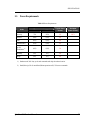
3.4 Performance Specifications
Table 3-4 Performance Specifications
DESCRIPTION SV2001H SV3012H SV4002H SV6003H SV6014H SV8004H
Seek Time (Rd/Wt, typical):
Average seek time
Track to track seek time
Full stroke seek time
8.9/10.0 msec
0.8/1.0 msec
16.5/17.5 msec
Data Transfer Rate: (Maximum)
buffer to/from media
host to/from buffer
443 Mbits/s
16.6/33/66/100 Mbytes/s
Average latency 5.56 msec
Rotational Speed 5,400 ± 0.35% rpm
Motor spin up time (Typical) 10 sec
Motor spin down time (Typical) 7 sec
Buffer size 2048 Kbytes
NOTES: ∗ Seek time is defined as the time from the receipt of a read, write or seek command until
the actuator has repositioned and settled on the desired track with the drive operating at
nominal DC input voltages and nominal operating temperature.
∗ Average seek time is determined by averaging the time to complete 1,000 seeks of
random length.
∗ Average latency is the time required for the drive to rotate1/2 of a revolution and on
average is incurred after a seek completion prior to reading or writing user data.
∗ Spin up time is the time elapsed between the supply voltages reaching operating range
and the drive being ready to accept all commands.

SPECIFICATIONS
SpinPoint V40 Product Manual
9
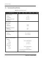
3.5 Power Requirements
Table 3-5 Power Requirements
Typical Current (mA rms)
Mode
+5 Volts
+12 Volts
Typical Power
(Watts)
Maximum
Power (Watts)
Spin-up 750 2070 26 28.71
Normal (400) (235) 4.8
Idle (415) (225) 4.8
Random Seek
(1)
(410) (320) 6.0
@ OD
Read/Write
(2)
(425) (225) 5.0
Standby (60) (15) 0.8
Sleep (60) (15) 0.8
1) Random seek: 30% Duty cycle seek commands with logical random location.
2) Read/Write @ OD: On track Read/Write operation at OD, 256 sector commands.

SPECIFICATIONS
SpinPoint V40
Product Manual
10
3.6 Environmental Specifications
Table 3-6 Environmental Specifications
DESCRIPTION SV2001H SV3012H SV4002H SV6003H SV6014H SV8004H
Ambient Temperature:
Operating
Non-operating
Maximum gradient without
Condensation
5 ∼ 55°C
-40 ∼ 70°C
20°C/15%/hr
Relative Humidity
(non-condensing):
Operation
Non-operation
Maximum wet bulb temperature:
Operating
Non-operating
5~85 %
5~95 %
30° C
40° C
Altitude (relative to sea level):
Operating
Non-operating
-650 ∼ 10,000 feet
-1,000 ∼ 40,000 feet
Vibration (1/2 oct/min sweep sine):
Operating
5-21Hz
21-300Hz
300-500Hz
Non-operating
5-21Hz
21-500Hz
0.034" (double amplitude)
1.5 G (P-P) *
0.5 G (P-P) **
0.195" (double amplitude)
8.0 G (p-p)
* No more than 20% throughput degradation
** No error during test

SPECIFICATIONS
SpinPoint V40 Product Manual
11
Table 3-6 Environmental Specifications (continued)
DESCRIPTION SV2001H SV3012H SV4002H SV4002H SV6014H SV6003H
Shock (1/2 sine pulse);
Operating
2.0 ms
Non-operating
2.0 ms
1.0 ms
0.5 ms
Rotational Shock
Operating
2.0 ms
Non-operating
2.0 ms
1.0 ms
63G
350G
150G
200G
2K rad/sec
2
20K rad/sec
2
20K rad/sec
2
Acoustic Noise
(Typical Sound Power)
Idle
Random Read/Write
Quite Seek
3.1 bels
3.3 bels
3.1 bels
3.7 Reliability Specifications
Table 3-7 Reliability Specifications
DESCRIPTION SV2001H SV3012H SV4002H SV4002H SV6014H SV8004H
Recoverable Read Error:
<10 in 10
11
bits
Non-
Recoverable Read Error:
<1 sector in 10
14
bits
MTBF (POH): 500,000 hours
MTTR (typical): 5 minutes
Start/Stop Cycles:
Ambient
Stressed
50,000
30,000
Component Design Life: 5 years

INSTALLATION
SpinPoint V40
Product Manual
12
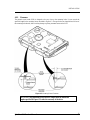
CHAPTER 4 INSTALLATION
This chapter describes how to unpack, mount, configure, and connect a SpinPoint V40 hard disk drive. It also
describes how to install the drive in systems.
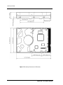
4.1 Space Requirements
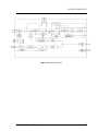
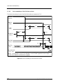
Figure 4-1 shows the external dimensions of the drive.
Figure 4-1 Mechanical Dimension
Page is loading ...
Page is loading ...
Page is loading ...
Page is loading ...
Page is loading ...
Page is loading ...
Page is loading ...
Page is loading ...
Page is loading ...
Page is loading ...
Page is loading ...
Page is loading ...
Page is loading ...
Page is loading ...
Page is loading ...
Page is loading ...
Page is loading ...
Page is loading ...
Page is loading ...
Page is loading ...
Page is loading ...
Page is loading ...
Page is loading ...
Page is loading ...
Page is loading ...
Page is loading ...
Page is loading ...
Page is loading ...
Page is loading ...
Page is loading ...
Page is loading ...
Page is loading ...
Page is loading ...
Page is loading ...
Page is loading ...
Page is loading ...
Page is loading ...
Page is loading ...
Page is loading ...
Page is loading ...
Page is loading ...
Page is loading ...
Page is loading ...
Page is loading ...
Page is loading ...
Page is loading ...
Page is loading ...
Page is loading ...
Page is loading ...
Page is loading ...
Page is loading ...
Page is loading ...
Page is loading ...
Page is loading ...
Page is loading ...
Page is loading ...
Page is loading ...
Page is loading ...
Page is loading ...
Page is loading ...
Page is loading ...
Page is loading ...
Page is loading ...
Page is loading ...
Page is loading ...
Page is loading ...
Page is loading ...
Page is loading ...
Page is loading ...
Page is loading ...
Page is loading ...
Page is loading ...
Page is loading ...
Page is loading ...
Page is loading ...
Page is loading ...
Page is loading ...
Page is loading ...
Page is loading ...
Page is loading ...
Page is loading ...
Page is loading ...
Page is loading ...
Page is loading ...
Page is loading ...
Page is loading ...
Page is loading ...
Page is loading ...
Page is loading ...
Page is loading ...
Page is loading ...
Page is loading ...
Page is loading ...
Page is loading ...
Page is loading ...
-
 1
1
-
 2
2
-
 3
3
-
 4
4
-
 5
5
-
 6
6
-
 7
7
-
 8
8
-
 9
9
-
 10
10
-
 11
11
-
 12
12
-
 13
13
-
 14
14
-
 15
15
-
 16
16
-
 17
17
-
 18
18
-
 19
19
-
 20
20
-
 21
21
-
 22
22
-
 23
23
-
 24
24
-
 25
25
-
 26
26
-
 27
27
-
 28
28
-
 29
29
-
 30
30
-
 31
31
-
 32
32
-
 33
33
-
 34
34
-
 35
35
-
 36
36
-
 37
37
-
 38
38
-
 39
39
-
 40
40
-
 41
41
-
 42
42
-
 43
43
-
 44
44
-
 45
45
-
 46
46
-
 47
47
-
 48
48
-
 49
49
-
 50
50
-
 51
51
-
 52
52
-
 53
53
-
 54
54
-
 55
55
-
 56
56
-
 57
57
-
 58
58
-
 59
59
-
 60
60
-
 61
61
-
 62
62
-
 63
63
-
 64
64
-
 65
65
-
 66
66
-
 67
67
-
 68
68
-
 69
69
-
 70
70
-
 71
71
-
 72
72
-
 73
73
-
 74
74
-
 75
75
-
 76
76
-
 77
77
-
 78
78
-
 79
79
-
 80
80
-
 81
81
-
 82
82
-
 83
83
-
 84
84
-
 85
85
-
 86
86
-
 87
87
-
 88
88
-
 89
89
-
 90
90
-
 91
91
-
 92
92
-
 93
93
-
 94
94
-
 95
95
-
 96
96
-
 97
97
-
 98
98
-
 99
99
-
 100
100
-
 101
101
-
 102
102
-
 103
103
-
 104
104
-
 105
105
-
 106
106
-
 107
107
-
 108
108
-
 109
109
-
 110
110
-
 111
111
-
 112
112
-
 113
113
-
 114
114
-
 115
115


Samsung SPINPOINT V40 Series User manual
- Category
- Internal hard drives
- Type
- User manual
Ask a question and I''ll find the answer in the document
Finding information in a document is now easier with AI
Related papers
Other documents
-
Integral INSSD64GP25MXZ Datasheet
-
-
-
-
-
Integral INAFM8G40VSXE User manual
-
Seagate Samsung Spinpoint M Series User manual
-
Toshiba MK6017MAP User manual
-
takeMS MS128SDC010 Datasheet
-