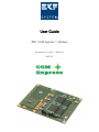
EKF XB1 COM Express User manual
- Category
- Network switches
- Type
- User manual
This manual is also suitable for

User Guide
XB1 COM Express™ Module
Document No. 4162 • Edition 5
2007-05
COM
Ex
p
res
s

User Guide XB1 COM Express Module
©EKF -2- ekf.com
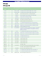
Contents
About this Manual ........................................................... 4
Edition History......................................................... 4
Related Documents ..................................................... 5
Nomenclature ......................................................... 5
Trade Marks .......................................................... 5
Legal Disclaimer - Liability Exclusion ......................................... 5
XB1 COM Express Module Features .............................................. 6
Feature Summary ...................................................... 6
Short Description XB1 COM Express Module .................................. 8
Block Diagram XB1 COM Express Module ................................... 10
Assembly Drawing XB1 COM Express Module ................................ 11
Strapping Headers ..................................................... 12
Connectors & Sockets .................................................. 12
Indicators ........................................................... 12
Microprocessor ....................................................... 13
Thermal Considerations ................................................. 14
Main Memory ........................................................ 15
LAN Subsystem ....................................................... 15
Serial ATA Interface (SATA) .............................................. 16
Enhanced IDE Interface (PATA) ........................................... 16
Graphics Subsystem ................................................... 17
Real-Time Clock....................................................... 18
Universal Serial Bus (USB) ............................................... 18
LPC Super-I/O Interface ................................................. 18
Firmware Hub (Flash BIOS) .............................................. 18
Watchdog/Reset ...................................................... 19
PG (Power Good) LED .................................................. 19
GP (General Purpose) LED ............................................... 19
Installing and Replacing Components ............................................ 20
Before You Begin...................................................... 20
Installing the Board .................................................... 21
Removing the Board ................................................... 22
EMC Recommendations................................................. 23
Installing or Replacing the Memory Modules ................................. 24
Replacement of the Battery .............................................. 24
Technical Reference ......................................................... 25
Local PCI Devices ...................................................... 25
Local SMB Devices ..................................................... 26
Hardware Monitor LM87 ................................................ 26
GPIO Usage.......................................................... 27
GPIO Usage ICH6 ................................................ 27
GPIO Usage FWH ................................................ 28
GPIO Usage SIO ................................................. 29
Configuration Jumpers ................................................. 30
Reset Jumper BIOS CMOS RAM Values (J-GP) ........................... 30
Reset Jumper ICH6 RTC Core (J-RTC) .................................. 30

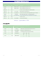
User Guide XB1 COM Express Module
©EKF -3- ekf.com
Connectors .......................................................... 31
PLD Programming Header ISPCON ................................... 31
J-COM ........................................................ 32
Processor Debug Header PITP ....................................... 36
P-SIO ......................................................... 37
Board Dimensions ..................................................... 38
Top View, Bottom View................................................. 39
Literature ........................................................... 40

User Guide XB1 COM Express Module
©EKF -4- ekf.com
About this Manual
This manual describes the technical aspects of the XB1 COM Express Module, required for installation
and system integration. It is intended for the experienced user only.
Edition History
Ed.
Contents/Changes
Author Date
1 User Manual XB1 COM Express Module, English, initial edition (Text #4162,
File: xb1_uge.wpd)
jj 27 April 2006
2 Table J-COM modified (PCIe Lane #3) jj 1 August 2006
3 Illustration 'Assembly Drawing' jj 31 August
2006
4 Added XB1 photographs jj 16 November
2006
5 Added XB1-060 jj 2 May 2007

User Guide XB1 COM Express Module
©EKF -5- ekf.com
Related Documents
For ordering information refer to document XB1 COM Express Module Product Information, available
at http://www.ekf.com/x/xb1/xb1_pie.pdf.
Nomenclature
Signal names used herein with an attached '#' designate active low lines.
Trade Marks
Some terms used herein are property of their respective owners, e.g.
< Intel, Pentium, Celeron, SpeedStep: ® Intel
< PCI Express: ® PCI-SIG
< COM Express:™ PICMG
< CompactPCI, CompactPCI Express, PICMG: ® PICMG
< Windows (2000, XP, Vista etc): ® Microsoft
< EKF, ekf system: ® EKF
EKF does not claim this list to be complete.
Legal Disclaimer - Liability Exclusion
This manual has been edited as carefully as possible. We apologize for any potential mistake.
Information provided herein is designated exclusively to the proficient user (system integrator,
engineer). EKF can accept no responsibility for any damage caused by the use of this manual.

User Guide XB1 COM Express Module
©EKF -6- ekf.com
XB1 COM Express Module Features
Feature Summary
Feature Summary XB1
Form Factor PICMG COM Express R1.0 (COM.0), Basic Module form factor (125x95mm
2
),
Pin-out Type 2
Processor Designed for Intel® Pentium® M Micro FC-BGA 479 processors (90nm
Dothan), maximum junction temperature 100°C
< XB1-060: 600MHz ULV Celeron® M (Banias 130nm), 400MHz FSB, 512KB
L2 cache, 7W
< XB1-100: 1.0GHz ULV Celeron® M (Dothan 373), 400MHz FSB,
512KB L2 cache, 5W
< XB1-140: 1.4GHz LV Pentium® M (Dothan 738), 400MHz FSB, 2MB
L2 cache, 10W
< XB1-200: 2.0GHz Pentium® M (Dothan 760), 533MHz FSB, 2MB L2
cache, 27W
Chipset Intel® i915 embedded systems chipset (Alviso) consisting of:
< 82915GM Graphics/Memory Controller Hub (GMCH) with Intel®
Graphics Media Accelerator (GMA) 900
< 82801FB I/O Controller Hub (ICH6)
< 82802 Compatible Firmware Hub (FWH)
Memory Dual 200-pin SO-DIMM socket, DDR2 533 SDRAM, 2 x 1GB maximum,
symmetric dual channel capable
Video Up to 2048x1536 pixel 16M colours @75Hz refresh rate (analog), up to
1600 x 1200 pixel 16M colours @60Hz (digital), dual screen support
< Dual SDVO
< Analog VGA
< Dual LVDS
< TV Out
< PEG PCI Express x 16 external graphics interface, multiplexed with
SDVO
USB 8 x USB2.0
Ethernet PCIe to Gigabit Ethernet controller 10/100/1000Mbps
PATA (IDE) ICH6 integrated Ultra ATA/100 I/F
SATA 4 x SATA-150
GPIO 8 GPIO lines
Sound System AC '97 or HD Audio Azalia (external Codec)
PCI ICH6 integrated 32-bit PCI bridge, 133MBps CPCI master
PCI Express 3-Lane PCIe if PCIe Gigabit Ethernet controller is stuffed
4-Lane PCIe (x 4 Link) w/o PCIe Gigabit Ethernet controller (stuffing option)
BIOS Phoenix BIOS

User Guide XB1 COM Express Module
Feature Summary XB1
©EKF -7- ekf.com
Drivers < Intel graphics drivers
< Intel networking drivers
Power
Requirements
+12V ±0.5V, tbd A max. @2.0GHz (tbd A WinXP idle mode)
Environmental
Conditions
< Operating temperature: 0°C ... +70°C (CPU dependent)
< Storage temperature: -40°C ... +85°C, max. gradient 5°C/min
< Humidity 5% ... 95% RH non condensing
< Altitude -300m ... +3000m
< Shock 15g 0.33ms, 6g 6ms
< Vibration 1g 5-2000Hz
MTBF tbd
EC Regulations • EN55022, EN55024, EN60950-1 (UL60950-1/IEC60950-1)
• 2002/95/EC (RoHS)
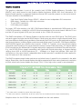
Performance
Rating
Measured with
PCMark2005
Board Processor CPU/MEM
Score
XB1-060
600MHz ULV Celeron® M (Banias) tbd
XB1-100
1.0GHz ULV Celeron® M (Dothan 373) tbd
XB1-140
1.4GHz LV Pentium® M (Dothan 738) tbd
XB1-201
2.0GHz Pentium® M (Dothan 760) tbd
Subject to technical changes
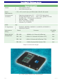
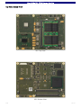
XB1 COM Express Module with Heatspreader

User Guide XB1 COM Express Module
©EKF -8- ekf.com
Short Description XB1 COM Express Module
COM Express™ (also known as ETXexpress™) is
an open PICMG
®
standard for Computer-On-
Modules, comprising of latest technologies such
as PCI Express, Serial ATA, Gigabit Ethernet and
SDVO. While designing the carrier board only
once, users profit from upgrading or scaling
their application by simply changing the CPU
module.
Alternatively equipped with the Intel series of
(LV) Pentium® M and ULV Celeron® M
processors and up to 2GB RAM, the EKF
XB1 is
a versatile COM Express basic form factor
module, designed especially for systems which
require high performance at low power
consumption.
The chipset is based on PCI Express
technology and has integrated a powerful dual
screen graphics accelerator. The SDVO and VGA
video interfaces allow for attachment of digital flat
panel displays and analog monitors.
The XB1 is provided with a Gigabit Ethernet
controller, and eight USB 2.0 ports for high speed
communication. Four Serial ATA channels are
available in addition to the legacy PATA I/F. The dual
slot DIMM socket is suitable to address up to 2GB
interleaved (symmetric) dual channel memory.
Typically, the XB1 will be combined with a custom
specific carrier board. As a basic development tool,
EKF can supply a third party evaluation carrier board.
In addition, EKF offers their design services to create
a turn-key ready customer solution.
The XB1 COM Express module is the perfect choice
for embedded applications that require a low power
standard processor at the centre of their design.
OEMs can significantly improve their flexibility and
reduce their total cost by adopting the open
standards based architecture of COM Express.
XB1 COM Express Module

User Guide XB1 COM Express Module
©EKF -9- ekf.com
Benefits of the XB1 COM Express Module
< PICMG COM.0 Compliant Module Type 2
< Pentium® M 2GHz (FSB 533MHz)
< PCI Express Chipset for Embedded Applications
< 2 x 1GB DDR2 Memory (Dual Channel Mode Capable)
< Dual-Screen Graphics Controller
< Video I/F SDVO, PEG, LVDS, VGA, TV
< Gigabit Ethernet Controller
< 4 x SATA I/F
< 8 x USB 2.0 Channels
< RoHS Compliant
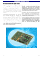
XB1 from Bottom

User Guide XB1 COM Express Module
©EKF -10- ekf.com
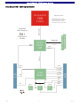
Block Diagram XB1 COM Express Module
SO-DIMM 200
Simplified
Block Diagram
COM Express
Module
X
B1
Pentium® M
2.0GHz
760
SO-DIMM 200
82
802
87
61
BIOS
SIO
G-ETH
SDVO
PEG
PEG
VGA
LVDS/TV
3 x PCIe
PCIeLPC
AC '97
DDR2 533
512MB-2GB
Dual
Channel
FSB 533MHz
GMCH
82915
GM
ICH6
82801
4 x SATA
8 x USB
GBE
DMI x 4
VGA
LPC
IDE
SDVO
PCI
A-B
SMB
GPIO
C-D
82
573
Alternative CPU:
• Pentium® M 745 1.8GHz
• LV Pentium® M 738 1.4GHz
• Celeron® M 370 1.5GHz
• ULV Celeron® M 373 1.0GHz

User Guide XB1 COM Express Module
©EKF -11- ekf.com
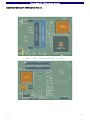
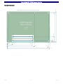
Assembly Drawing XB1 COM Express Module
GMCH
J-GP
GP
LED
PG
J-RTC
© EKF • B1 COM Express Module • ekf.com
X
X
B1
Top
© EKF
ekf.com
X
B1
Bottom
© EKF
ekf.com
CPU
DDR2 SODIMM
DDR2 SODIMM
+
BAT
ICH
P-SIO
A1
C1
D1
B1
COM Express Module Connector
J-COM A-B
J-COM C-D
P-ITP
ISPCON
1
1
1
NIC
SIO
FWH
isp
GAL

User Guide XB1 COM Express Module
©EKF -12- ekf.com
Strapping Headers
J-GP Jumper to reset BIOS CMOS RAM values
J-RTC Jumper to reset RTC core of ICH6, not stuffed
Connectors & Sockets
ISPCON PLD programming connector, not stuffed
J-COM A-B COM Express connector rows A and B (VGA, LVDS, TV, PCIe, SATA,
Ethernet, USB, AC'97, SMB, LPC)
J-COM C-D COM Express connector rows C and D (Dual SDVO / PEG, IDE, PCI)
P-ITP CPU debug port
P-SIO I/O connector for debugging (not stuffed), comprises PS/2
mouse/keyboard signals, UART (TTL)
SODIMM1
SODIMM2
200-pin DDR2 SDRAM PC2-3200/4200 (DDR400/533) 1.8V memory
module sockets
Indicators
GP General Purpose LED
PG LED indicating Power Good / Board Healthy

User Guide XB1 COM Express Module
©EKF -13- ekf.com
Microprocessor
The XB1 COM Express Module is designed for use with Pentium® M and Celeron® M processors
manufactured in 90nm technology (Dothan). These include also the Ultra Low-Voltage (ULV)
Celeron® M and the Low-Voltage (LV) Pentium® M processors as listed below. The processors are
housed in a Micro FC-BGA package for direct soldering to the PCB, i.e. the CPU chip cannot be
removed or changed by the user.
The processors supported by the XB1 COM Express Module are running at FSB clock speeds of
400MHz and 533MHz. The internal Pentium M processor speed is achieved by multiplying the host
bus frequency by a variable value. The multiplier is chosen by currently required performance and the
actual core temperature. This technology is called Enhanced Intel SpeedStep®.
Power is applied across the COM Express connectors J-COM (+12V). The processor core voltage is
generated by a switched voltage regulator. The processor signals its required core voltage by 6
dedicated pins according to Intels IMVP-IV voltage regulator specification.
90nm (Dothan) Processors Supported
Processor Speed
min/max
[GHz]
Host Bus
[MHz]
L2 Cache
[MB]
TDP
[W]
Die Temp
[°C]
CPU ID Stepping sSpec
ULV Celeron M 373
1)
2)
1.0/1.0 400 0.5 5 0-100 06D8h C-0 SL8LW
LV Pentium M 738
2)
0.6/1.4 400 2 10 0-100 06D6h
06D8h
B-1
C-0
SL7P9
SL89N
Pentium M 745
2)
0.6/1.8 400 2 21 0-100 06D6h
06D8h
B-0
C-0
SL7Q6
SL8U8
Pentium M 760
2)
0.8/2.0 533 2 27 0-100 06D8h C-0 SL869
1)
This processor does not support SpeedStep® technology, instead it runs at a fixed core speed
2)
Following the Intel Embedded Roadmap, this processor is recommended for long time availability

User Guide XB1 COM Express Module
©EKF -14- ekf.com
Thermal Considerations
In order to avoid malfunctioning of the XB1 COM Express Module, take care of appropriate cooling
of the processor and system, e.g. by a cooling fan suitable to the maximum power consumption of
the CPU chip actually in use. Please note, that the processors temperature is steadily measured by a
special controller (LM87), attached to the onboard SMBus
®
(System Management Bus). A second
temperature sensor internal to the LM87 allows for acquisition of the boards surface temperature.
Beside this the LM87 also monitors most of the supply voltages. A suitable software to display both,
the temperatures as well as the supply voltages, is MBM (Motherboard Monitor), which can be
downloaded from the web. After installation, both temperatures and voltages can be observed
permanently from the Windows taskbar.
The XB1 COM Express Module is equipped with a passive heatsink (heat-spreader). In addition, a
forced airflow through the system enclosure by a suitable fan unit is highly recommended (>15m
3
/h
or 200LFM around the CPU module). As an exception, the XB1-100 (ULV Celeron M 1GHz) can be
operated with natural convection only. Be sure to thoroughly discuss your actual cooling needs with
EKF. Generally, the faster the CPU speed the higher its power consumption. For higher ambient
temperatures, consider increasing the forced airflow to 400 or 600LFM.
The table showing the supported processors above give also the maximum power consumption (TDP
= Thermal Design Power) of a particular processor. Fortunately, the power consumption is by far
lower when executing typical Windows or Linux tasks. The heat dissipation may increase considerably
when e.g. rendering software such as the Acrobat Distiller is executed.
The Pentium M processors support Intel's Enhanced SpeedStep® technology. This enables dynamic
switching between multiple core voltages and frequencies depending on core temperature and
currently required performance. The processors are able to reduce their core speed and core voltage
in up to 8 steps down to 600MHz. This leads to an obvious reduction of power consumption (max.
7.5W @600MHz) resulting in less heating. This mode of lowering the processor core temperature is
called TM2 (TM=Thermal Monitor). Note, that TM2 is not supported by Celeron M processors.
Another way to reduce power consumption is to modulate the processor clock. This mode (TM1) is
supported also by the Celeron M processors and is achieved by actuating the 'Stop Clock' input of the
CPU. A throttling of 50% e.g. means a duty cycle of 50% on the stop clock input. However, while
saving considerable power consumption, the data throughput of the processor is also reduced. The
processor works at full speed until the core temperature reaches a critical value. Then the processor
is throttled by 50%. As soon as the high temperature situation disappears the throttling will be
disabled and the processors runs at full speed again.
A similar feature is embedded within the Graphics and Memory Controller (GMCH) i915GM. An on-
die temperature sensor is used to protect the GMCH from exceeding its maximum junction
temperature (T
J,max
=105°C) by reducing the memory bandwidth.
These features are controllable by BIOS menu entries. By default the BIOS of the XB1 COM Express
Module enables mode TM2 which is the most efficient.

User Guide XB1 COM Express Module
©EKF -15- ekf.com
Main Memory
The XB1 COM Express Module is equipped with two sockets for installing 200-pin SO-DIMM modules
(module height = 1.25 inch). Supported are unbuffered DDR2 SO-DIMMs (V
CC
=1.8V) without ECC
featuring on-die termination (ODT), according the PC2-3200 or PC2-4200 specification. Minimum
memory size is 128MB; maximum memory size is 2GB. Due to the video requirements of the i915GM
chipset (some of the system memory is dedicated to the graphics controller), a minimum of 2x256MB
memory is recommended for the operating systems Windows NT 4.0, Windows 2000 or Windows XP.
The contents of the SPD EEPROM on the SO-DIMMs are read during POST (Power-on Self Test) to
program the memory controller within the chipset.
The i915GM chipset supports symmetric and asymmetric memory organization. The maximum
memory performance can be obtained by using the symmetric mode. To achieve this mode, two
SO-DIMMs of equal capacity must be installed in the memory sockets. In asymmetric mode different
memory modules may be used with the drawback of less bandwidth. A special case of asymmetric
mode is to populate only one memory module (i.e. one socket may be left empty).
LAN Subsystem
The Ethernet LAN subsystem is comprised of the Intel 82573 Gigabit Ethernet controller, which
provides also legacy 10Base-T and 100Base-TX connectivity.
< Single PCI Express lane linkage
< 1000Base-Tx (Gigabit Ethernet), 100Base-TX (Fast Ethernet) and 10Base-T (Classic Ethernet)
capability
< Half- or full-duplex operation
< IEEE 802.3u Auto-Negotiation for the fastest available connection
< Jumperless configuration (completely software-configurable)
The NIC (Networking Interface Controller) is connected by a single PCI Express lane to the chipset
southbridge (ICH6). Its MAC address (unique hardware number) is stored in a dedicated EEPROM. The
Intel Ethernet software and drivers for the 82573 is available from Intel's World Wide Web site for
download (link provided on the EKF website).
By specification, the XB1 COM Express Module does not provide any I/O connector. Instead, the
carrier board must provide the RJ45 receptacle with integrated magnetics for copper twisted pair
Ethernet. All MDI (Media Dependent Interface) signals of the Ethernet PHY are routed to the
connector J-COM A-B.
The 82573 controller is connected to the PCI Express lane #3. As an alternate stuffing option, this
lane is available across the J-COM connector instead, for carrier board applications which require 4
PCIe lanes (typically configured as PCIe x 4 link). If this stuffing option had been ordered, no Ethernet
connectivity is provided on the XB1 itself, but may be replicated on the carrier board.

User Guide XB1 COM Express Module
©EKF -16- ekf.com
Serial ATA Interface (SATA)
The XB1 COM Express Module provides four serial ATA (SATA) ports, each capable of transferring
150MB/s. Integrated within the ICH6, the SATA controller features different modes to support also
legacy operating systems. The SATA channels are available to the carrier board across the J-COM A-B
connector.
Available for download from Intel are drivers for popular operating systems, e.g. Windows® 2000,
Windows® XP and Linux.
Enhanced IDE Interface (PATA)
The parallel ATA (PATA, also known as IDE) interface is provided for attachment of legacy peripheral
devices such as hard disks, ATA CompactFlash cards and CD-ROM drives. The interface supports:
C Up to two ATA devices
C PIO Mode 3/4, Ultra ATA/33, Ultra ATA/66, Ultra ATA/100
The PATA port is available to the carrier board across the J-COM C-D connector. The IDE controller is
integrated into the ICH6. Ultra ATA IDE drivers can be downloaded from the Intel website.

User Guide XB1 COM Express Module
©EKF -17- ekf.com
Graphics Subsystem
The graphics subsystem is part of the versatile Intel i915GM Graphics/Memory Controller Hub
(GMCH), and is also known as Intel Graphics Media Accelerator (GMA) 900. As an alternative, PCI
Express based graphics is supported (requires discrete PEG controller present on the carrier board).
The main features of the GMA900 are:
< Dual Serial Digital Video Output (SDVO) - allows for two independent DVI connectors
< RGB output - suitable for a VGA style connector
< TV out (HDTV resolution)
< LVDS wide panel support
For legacy CRT style monitors, the XB1 COM Express Module is provided with RGB signals on the
J-COM A-B connector, suitable for a VGA D-Sub accommodated on the carrier board. Also the TV out
and the LCD panel signals (LVDS port) are routed to the J-COM A-B connector.
The GMCH multiplexes a PCI Express Graphics interface with two Intel SDVO ports. The SDVO ports
can each support a single-channel SDVO device. If both ports are active in single-channel mode, they
can have different display timing and data. Alternatively the SDVO ports can be combined to support
dual channel devices, enabling higher resolutions and refresh rates. On the XB1 COM Express Module,
the SDVO/PEG signals are routed to the connector J-COM C-D. Typically, one or two discrete display
transmitter chips located on the carrier board are used to convert Intels proprietary, PCI express based
SDVO interfaces to the differential DVI signals required for attachment of modern flat panel monitors.
E.g., the SiI1362 (Silicon Image) transmitter uses PanelLink® Digital technology to support displays
ranging from VGA to UXGA resolutions (25 - 165Mpps) in a single link interface. With two DVI
connectors on the carrier board, independent dual screen operation is available (this also applies for
one DVI and one D-Sub connector).
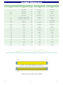
The GMCH supports several video resolutions and refresh rates. A partial list is contained in the table
below. Please note, that flat-panel displays should be operated with their native (maximum) resolution
at 60Hz refresh rate (some models also accept 75Hz). 16-bit high colour mode is recommended.
Partial List of i915GM GMCH Video Modes (analog / digital)
Resolution 60Hz 70Hz 72Hz 75Hz 85Hz
640x480 T / TT / TT / TT / TT / T
800x600 T / TT / TT / TT / TT / T
1024x768 T / T
1)
T / TT / TT / TT / T
1280x1024 T / T
1)
T / TT / TT / TT / T
1600x1200 T / T
1)
2)
T / - T / - T / - T / -
2048x1536 T / - T / - T / - T / - - / -
1)
This video mode is suitable for popular flat-panel displays
2)
In dual screen mode 2 x 1600x1200, 32-bit true colours are not available for both outputs simultaneously
Graphics drivers for the i915GM can be downloaded from the Intel website.

User Guide XB1 COM Express Module
©EKF -18- ekf.com
Real-Time Clock
The XB1 COM Express Module has a time-of-day clock and 100-year calendar, integrated into the
ICH6.
A battery on the board keeps the clock current when the computer is turned off. The XB1 uses a
Vanadium-Pentoxide-Lithium rechargeable battery, giving an autonomy of more than 50 days when
fully loaded after 24 hours. The cell is free of memory effects and withstands deep discharging. Under
normal conditions, replacement should be superfluous during lifetime of the board. Custom specific
versions of the XB1 may not provide the accumulator.
In addition, VCC_RTC is also redundantly derived from the carrier board (if supported). The time
keeping autonomy period is then defined by the battery capacity accommodated on the carrier.
Universal Serial Bus (USB)
The XB1 COM Express Module is provided with eight USB ports, all of them are USB 2.0 capable. Four
active-low over-current sensing inputs are available in addition, suitable for attachment of electronic
switches such as the LM3526-L on the carrier board. The USB controllers are integrated into the ICH6.
LPC Super-I/O Interface
In a modern system, legacy ports as PS/2 keyboard/mouse, COM1/2 and LPT have been replaced by
USB and Ethernet connectivity. The 1.4MB floppy disk drive has been swapped against CD/DVD-RW
drives or USB memory sticks. Hence, the XB1 COM Express Module is virtually provided with all
necessary I/O functionality. However, for BIOS and OS software compatibility, the XB1 is additionally
equipped with a simple Super-I/O chip. The Super-I/O controller resides on the local LPC bus (LPC =
Low Pin Count interface standard), which is a serialized ISA bus replacement. For debug only, a
connector P-SIO may be stuffed on the XB1, with KB/MS signals derived from the SIO and also a
rudimentary serial I/F (TTL-level Tx/Rx RTS/CTS).
The SIO provides a rich set of GPIO lines. Four channels are used as GPI0..3, and another 4 channels
as GPO0..3, all routed to the connector J-COM A-B, for use on the carrier board.
Firmware Hub (Flash BIOS)
The BIOS is stored in an 8Mbit Firmware Hub attached to the LPC bus. The firmware hub contains a
nonvolatile memory core based on flash technology, allowing the BIOS to be upgraded. The XB1
firmware hub may be deselected by the carrier board from use as primary BIOS source, by activating
the signal BIOS_DISABLE# on J-COM A-B. This allows a potential secondary firmware hub residing on
the carrier board to be used as alternative BIOS source.
The FWH can be reprogrammed (if suitable) by a DOS based tool. This program and the latest XB1
COM Express Module BIOS are available from the EKF website. Read carefully the enclosed
instructions. If the programming procedure fails e.g. caused by a power interruption, the XB1 COM
Express Module may no more be operable. In this case you would have to send in the board, because
the BIOS is directly soldered to the PCB and cannot be changed by the user.

User Guide XB1 COM Express Module
©EKF -19- ekf.com
Watchdog/Reset
The XB1 COM Express Module is provided with two supervisor circuits to monitor the supply voltages
1.8V, 3.3V, 5V, and to generate a clean power-on reset signal. The healthy state of the XB1 COM
Express Module immideately after a reset is signalled by the LED PG (Power Good), indicating that all
power voltages are within their specifications and the reset signal has been deasserted.
An important reliability feature is the watchdog function, which is programmable by software. The
behaviour of the watchdog is defined within the PLD, which activates/deactivates the watchdog and
controls its time-out period. The time-out delay is adjustable in the steps 2, 10, 50 and 255 seconds.
After alerting the WD and programming the time-out value, the related software (e.g. application
program) must trigger the watchdog periodically. All watchdog related functions are made available
by calling service requests within the BIOS.
The watchdog is in a passive state after a system reset. There is no need to trigger it at boot time. The
watchdog is activated on the first trigger request. If the duration between two trigger requests
exceeds the programmed period, the watchdog times out and a system reset will be generated. The
watchdog remains in its active state until the next system reset. There is no way to disable it once it
had been put on alert, whwereas it is possible to reprogram its time-out value at any time.
PG (Power Good) LED
The XB1 COM Express Module offers a software programmable LED located. After system reset, this
LED defaults to signal the board healthy respectively power good. By the first setting of the GPO20 of
the ICH6 this LED changes its function and is then controlled only by the level of the GPO20 pin.
Setting this pin to 1 will switch on the LED. The PG LED remains in the programmable state until the
next system reset.
GP (General Purpose) LED
A second, programmable LED can be also observed from the front panel. The status of the GP LED is
controlled by the GPO18 output of the ICH6. Setting this pin to 1 will switch on the LED. As of
current, the GP LED is not dedicated to any particular hardware or firmware function (this may change
in the future).

User Guide XB1 COM Express Module
©EKF -20- ekf.com
Installing and Replacing Components
Before You Begin
Warnings
The procedures in this chapter assume familiarity with the general terminology associated with
industrial electronics and with safety practices and regulatory compliance required for using and
modifying electronic equipment. Disconnect the system from its power source and from
any telecommunication links, networks or modems before performing any of the
procedures described in this chapter. Failure to disconnect power, or telecommunication
links before you open the system or perform any procedures can result in personal injury
or equipment damage. Some parts of the system can continue to operate even though
the power switch is in its off state.
Caution
Electrostatic discharge (ESD) can damage components. Perform the procedures described in this
chapter only at an ESD workstation. If such a station is not available, you can provide
some ESD protection by wearing an antistatic wrist strap and attaching it to a
metal part of the system chassis or board front panel. Store the board only in its
original ESD protected packaging. Retain the original packaging (antistatic bag and
antistatic box) in case of returning the board to EKF for rapair.
Page is loading ...
Page is loading ...
Page is loading ...
Page is loading ...
Page is loading ...
Page is loading ...
Page is loading ...
Page is loading ...
Page is loading ...
Page is loading ...
Page is loading ...
Page is loading ...
Page is loading ...
Page is loading ...
Page is loading ...
Page is loading ...
Page is loading ...
Page is loading ...
Page is loading ...
Page is loading ...
-
 1
1
-
 2
2
-
 3
3
-
 4
4
-
 5
5
-
 6
6
-
 7
7
-
 8
8
-
 9
9
-
 10
10
-
 11
11
-
 12
12
-
 13
13
-
 14
14
-
 15
15
-
 16
16
-
 17
17
-
 18
18
-
 19
19
-
 20
20
-
 21
21
-
 22
22
-
 23
23
-
 24
24
-
 25
25
-
 26
26
-
 27
27
-
 28
28
-
 29
29
-
 30
30
-
 31
31
-
 32
32
-
 33
33
-
 34
34
-
 35
35
-
 36
36
-
 37
37
-
 38
38
-
 39
39
-
 40
40


EKF XB1 COM Express User manual
- Category
- Network switches
- Type
- User manual
- This manual is also suitable for
Ask a question and I''ll find the answer in the document
Finding information in a document is now easier with AI


Other documents
-
 Cables Direct RB-432 Datasheet
-
M-Cab 7070013 Datasheet
-
MiTAC PD10AI User manual
-
 DROK 2001708006 User manual
-
Juniper Ex SERIES Quick start guide
-
kontron COMe Eval Carrier2 T10 User guide
-
Texas Instruments Differential Passive Signal Switch on Computing (Rev. A) Application notes
-
Intel 915GM User manual
-
AOpen XC Cube Installation guide
-

