Linear Technology LT3045EDD-1 Paralleled Ultralow Noise Ultrahigh PSRR LDO Regulator User manual

Type
User manual

The Linear Technology LT3045EDD-1 Paralleled Ultralow Noise Ultrahigh PSRR LDO Regulator offers a combination of features that make it ideal for a wide range of applications. Its ultralow noise and ultrahigh power supply rejection ratio (PSRR) make it suitable for powering noise-sensitive circuits, while its 3.8V to 20V input voltage range and 2A output current capability make it a versatile choice for a variety of applications. Additionally, its programmable current limit and power good threshold provide added flexibility.

The Linear Technology LT3045EDD-1 Paralleled Ultralow Noise Ultrahigh PSRR LDO Regulator offers a combination of features that make it ideal for a wide range of applications. Its ultralow noise and ultrahigh power supply rejection ratio (PSRR) make it suitable for powering noise-sensitive circuits, while its 3.8V to 20V input voltage range and 2A output current capability make it a versatile choice for a variety of applications. Additionally, its programmable current limit and power good threshold provide added flexibility.

1
UG-1359 Rev A
DEMO MANUAL DC2637A
DESCRIPTION
LT3045EDD-1
20V, 2A, Paralleled Ultralow Noise,
Ultrahigh PSRR LDO Regulator
Demo circuit 2637A features four LT
®
3045EDD-1s in par-
allel, generating an ultralow noise, ultrahigh power supply
rejection ratio (PSRR) low dropout (LDO) regulator with
programmable current limit. DC2637A operates over an
input range of 3.8V to 20V, and is capable of delivering
up to 2A output current by paralleling four LT3045EDD-1s
with only 20mΩ ballast resistors.
The VIOC tracking function of the LT3045EDD-1 controls
an upstream switching converter to maintain a constant
voltage across the regulator and hence minimize power
dissipation. In the parallel configuration, connect the VIOC
pin of only one IC to the switching converter, while the
VIOC pins of the other ICs are left floating. The power
good feedback (PGFB) pin is used to set a programmable
power good threshold, and also activates the fast start-up
circuitry. The PGFB is set on only one IC when they are
paralleled. LT3045-1 also offers programmable current
limit functionality by connecting a resistor from ILIM to
All registered trademarks and trademarks are the property of their respective owners.
PERFORMANCE SUMMARY
GND on each device. Current monitoring is also achieved
by sensing the ILIM pin voltage.
Built-in protection includes reverse battery protection,
reverse current protection, internal current limit with fold-
back, and thermal limit with hysteresis.
The LT3045-1 data sheet gives a complete descrip-
tion of the device, operation and applications informa-
tion. The data sheet must be read in conjunction with
this demo manual for demonstration circuit 2637A. The
LT3045EDD-1 is assembled in a 12-lead (3mm × 3mm)
plastic DFN package with an exposed pad on the bottom-
side of the IC. Proper board layout is essential for maxi-
mum thermal performance.
Design files for this circuit board are available at
http://www.analog.com/DC2637A
Specifications are at TA = 25°C
PARAMETER CONDITIONS MIN TYP MAX UNITS
Input Voltage Range (VIN) IOUT = 500mA, VOUT = 3.3V
IOUT = 2A, VOUT = 3.3V
3.8
3.8
20
5.5*
VDC
VDC
Output Voltage (VOUT) VIN = 5V, IOUT = 2A 3.19 3.29 3.39 VDC
Shutdown Input Current (IIN) JP1 = OFF, VIN = 5V 1 µA
*The maximum input voltage for 2A load current is set by the 65°C temperature rise of LT3045-1 on the demo circuit. Higher input voltage can be reached
if larger copper area or force-air cooling is applied. The output current is also limited by the differential of input and output voltage, please refer the data
sheet for details.
Downloaded from Arrow.com.
2
UG-1359 Rev A
DEMO MANUAL DC2637A
QUICK START PROCEDURE
Demonstration circuit 2637A is easy to set up to evaluate
the performance of four LT3045EDD-1s in parallel. Refer
to Figure 1 for proper measurement equipment setup and
follow the procedure below:
1. Connect the load between the VOUT and GND terminals.
2. With the power off, connect the input power supply to
the VIN and GND terminals.
3. Make sure the shunt of JP1 is at ON option.
4. Apply 3.8V across VIN to GND. Draw 2A of load cur-
rent. The output voltage should be 3.29V ±3% (3.19V
to 3.39V).
5. Vary VIN from 3.8V to 20V and the load current up
to 2A.
NOTE: Make sure the power dissipation is below the
thermal limit.
6. Refer to Application Notes AN70 and AN159 for mea-
suring output noise and PSRR.
Figure 1. Test Procedure Setup Drawing for DC2637A
Downloaded from Arrow.com.Downloaded from Arrow.com.
3
UG-1359 Rev A
DEMO MANUAL DC2637A
1. Best PSRR Performance: PCB Layout for Input Trace
For applications utilizing the LT3045-1 for post-regulating
switching converters, placing a capacitor directly at the
LT3045-1 input results in AC current (at the switching fre-
quency) flowing near the LT3045-1. Without careful atten-
tion to PCB layout, this relatively high frequency switch-
ing current generates an electromagnetic field (EMF)
that couples to the LT3045-1 output, thereby degrading
its effective PSRR. While highly dependent on the PCB,
the switching pre-regulator, and the input capacitor size,
among other factors, the PSRR degradation can easily
be 30dB at 1MHz. This degradation is present even if the
LT3045-1 is de-soldered from the board, because it effec-
tively degrades the PSRR of the PC board itself. While
negligible for conventional low PSRR LDOs, LT3045-1’s
ultrahigh PSRR requires careful attention to higher order
parasitics in order to realize the full performance offered
by the regulator.
The LT3045-1 demo board alleviates this degradation in
PSRR by using a specialized layout technique. In Figure 2,
the input trace (VIN) is highlighted in red, and in Figure 3
the return path (GND) is also highlighted together with
input capacitor C3. Normally when an AC voltage is
applied to the input of the board, AC current flows on
this path, thus generating EMF. This EMF couples to out-
put capacitors (C1, C4, C6, C7) and related traces, mak-
ing the PSRR appear worse than it actually is. With the
input trace directly above the return path, the EMFs are in
opposite directions, and consequently cancel each other
out. Making sure these traces exactly overlap each other
maximizes the cancellation effect and thus provides the
maximum PSRR offered by the regulator.
PCB LAYOUT
Figure 2. Layer 3 of DC2637A Figure 3. Bottom Layer of DC2637A
Downloaded from Arrow.com.Downloaded from Arrow.com.Downloaded from Arrow.com.
4
UG-1359 Rev A
DEMO MANUAL DC2637A
2. Best AC Performance: PCB Layout for Output
Capacitors C1, C4, C6 and C7
For ultrahigh PSRR performance, the LT3045-1 bandwidth
is quite high (~1MHz), making it very close to the output
capacitor’s self-resonance frequency (~1.6MHz). There-
fore, it is very important to avoid adding extra impedance
(ESL and ESR) outside the feedback loop. To that end,
minimize the effects of PCB trace and solder inductance
by Kelvin connecting OUTS and SET pin capacitor (CSET)
GND directly to output capacitors (C2) terminals using
split capacitor techniques. In parallel configuration, for
each output cap, pad 4 connects to the OUTS pin and pad
1 connects to the GND side of the SET pin capacitor. With
only small current flowing through these connections, the
impact of solder joint/PCB trace inductance on stability
is eliminated. While the LT3045-1 is robust enough not
to oscillate if the recommended layout is not followed,
phase/gain margin and stability will degrade.
PCB LAYOUT
Figure 4. C2 and CSET Connections for Best Performance
3
2
4
1
C2
R
SET
C
SET
C1
OUT
IN
SET
LT3045-1
100µA
OUTS
PG
ILIM
GND
PGFB
EN/UV
V
OUT
V
IN
Downloaded from Arrow.com.Downloaded from Arrow.com.Downloaded from Arrow.com.Downloaded from Arrow.com.
5
UG-1359 Rev A
DEMO MANUAL DC2637A
PCB LAYOUT
Figure 5. Split Pads for Output Capacitors on Top Layer of DC2637A
Downloaded from Arrow.com.Downloaded from Arrow.com.Downloaded from Arrow.com.Downloaded from Arrow.com.Downloaded from Arrow.com.
6
UG-1359 Rev A
DEMO MANUAL DC2637A
PARTS LIST
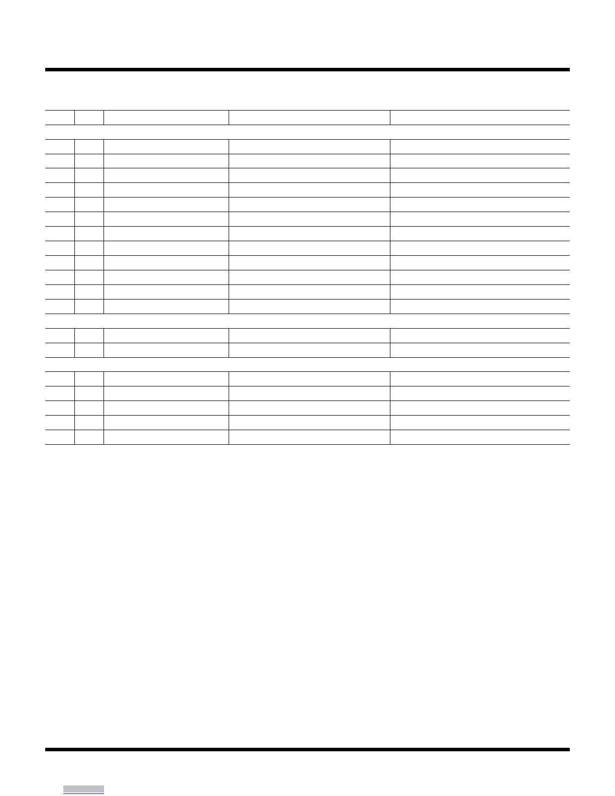
ITEM QTY REFERENCE PART DESCRIPTION MANUFACTURER/PART NUMBER
Required Circuit Components
1 4 C1, C4, C6, C7 CAP., 10µF, X5R, 25V, 10%, 1206 MURATA, GJ831CR61E106KE83L
2 1 C2 CAP., 22µF, 35V, 20%, 5X5.4mm SUN ELECTRONIC INDUSTRIES CORP, 35CE22BSS
3 3 C29, C30, C31 CAP., 0.47µF, X7R, 50V, 10%, 0805 MURATA, GRM21BR71H474KA88L
4 1 C3 CAP., 4.7µF, X7R, 50V, 10%, 1206 MURATA, GRM31CR71H475KA12L
5 1 C5 CAP., 4.7µF, X7R, 25V, 10%, 1206 MURATA, GRM31CR71E475KA88L
6 1 R18 RES., 200k, 1%, 1/10W, 0603 VISHAY, CRCW0603200KFKEA
7 4 R2, R3, R8, R9 RES., 0.02Ω, 1%, 1/5W, 0603 VISHAY, RCWE060320L0FQEA
8 4 R10, R12, R14, R16 RES., 249Ω, 1%, 1/10W, 0603 VISHAY, CRCW0603249RFKEA
9 1 R4 RES., 453k, 1%, 1/10W, 0603 VISHAY, CRCW0603453KFKEA
10 1 R6 RES., 49.9k, 1%, 1/10W, 0603 VISHAY, CRCW060349K9FKEA
11 1 R7 RES., 8.25k, 1%, 1/10W, 0805 VISHAY, CRCW06038K25FKEA
12 4 U1, U2, U3, U4 IC, LT3045EDD-1 12PIN DFN 3X3MM LINEAR TECHNOLOGY, LT3045-1EDD#PB
Additional Demo Board Circuit Components
1 1 C35, C40 CAP., OPTION, 1206
2 6 C26, C32, C34, C36, C37, C39 CAP., 0603, OPTION
Hardware: For Demo Board Only
1 5 E1, E2, E3, E4, E5 TEST POINT, TURRET, 0.094", MTG. HOLE MILL-MAX, 2501-2-00-80-00-00-07-0
2 1 JP1 CONN., HDR, MALE, 2x3, 2mm, THT, STR WURTH ELEKTRONIK, 62000621121
3 1 XJP1 CONN., SHUNT, FEMALE, 2 POS, 2mm WURTH ELEKTRONIK, 60800213421
4 2 J1, J2 CONN., RF, BNC, RCPT, THT, STR, 5-PIN AMPHENOL CONNEX, 112404
5 4 MH1, MH2, MH3, MH4 STANDOFF, NYLON, SNAP-ON, 0.250" WURTH ELEKTRONIK, 702931000
Downloaded from Arrow.com.Downloaded from Arrow.com.Downloaded from Arrow.com.Downloaded from Arrow.com.Downloaded from Arrow.com.Downloaded from Arrow.com.
7
UG-1359 Rev A
DEMO MANUAL DC2637A
Information furnished by Analog Devices is believed to be accurate and reliable. However, no responsibility is assumed by Analog
Devices for its use, nor for any infringements of patents or other rights of third parties that may result from its use. Specifications
subject to change without notice. No license is granted by implication or otherwise under any patent or patent rights of Analog Devices.
SCHEMATIC DIAGRAM
5
5
4
4
3
3
2
2
1
1
D
D
C
C
B
B
A
A
1. ALL RESISTORS AND CAPACITORS ARE 0603.
NOTES: UNLESS OTHERWISE SPECIFIED
*SEE DEMO MANUAL.
*
VIN
U1_EN
U1_SET
U1_EN
U1_SET
VIN
U1_EN
U1_SET
VIN
VIN
U1_EN
U1_SET
VIN
VIN
3.3V
U1_EN
VIN
U2
LT3045-1EDD
IN
1
IN
2
EN
4
PG
5
ILIM
6
OUT 11
OUTS 10
GND 9
SET 8
PGFB 7
GND
13
VIOC
3OUT 12
E2
GND
R7
8.25k
0805
C6
10uF
25V
1206
JP1
ON
OFF
1
3
2
C31
0.47uF
0805
50V
R16 249
U1
LT3045-1EDD
IN
1
IN
2
EN
4
PG
5
ILIM
6
OUT 11
OUTS 10
GND 9
SET 8
PGFB 7
GND
13
VIOC
3OUT 12
R18 200k
C7
10uF
25V
1206
R2 0.02
R3 0.02
R4
453k
C30
0.47uF
0805
50V
+
C2
22uF
35V
OPT
C5
4.7uF
1206
25V
U3
LT3045-1EDD
IN
1
IN
2
EN
4
PG
5
ILIM
6
OUT 11
OUTS 10
GND 9
SET 8
PGFB 7
GND
13
VIOC
3OUT 12
C1
10uF
25V
1206
R8 0.02
C34
OPT
E1
VIN
3.5V-20V
C36
OPT
C39
OPT
C40
OPT
1206
R14 249
U4
LT3045-1EDD
IN
1
IN
2
EN
4
PG
5
ILIM
6
OUT 11
OUTS 10
GND 9
SET 8
PGFB 7
GND
13
VIOC
3OUT 12
C37
OPT
R6
49.9k
J2
MONITOR
OUTPUT NOISE
C26
OPT
C4
10uF
25V
1206
J1
MONITOR
INPUT RIPPLE
R9 0.02
R12 249
E4
GND
C3
4.7uF
1206
50V
C32
OPT
E5
VIOC
E3
3.3V/2A
VOUT
C29
0.47uF
0805
50V
C35
1206
OPT
R10 249
Downloaded from Arrow.com.Downloaded from Arrow.com.Downloaded from Arrow.com.Downloaded from Arrow.com.Downloaded from Arrow.com.Downloaded from Arrow.com.Downloaded from Arrow.com.
8
UG-1359 Rev A
DEMO MANUAL DC2637A
ANALOG DEVICES, INC. 2017-2018
UG16974-0-5/18(A)
www.analog.com
ESD Caution
ESD (electrostatic discharge) sensitive device. Charged devices and circuit boards can discharge without detection. Although this product features patented or proprietary protection
circuitry, damage may occur on devices subjected to high energy ESD. Therefore, proper ESD precautions should be taken to avoid performance degradation or loss of functionality.
Legal Terms and Conditions
By using the evaluation board discussed herein (together with any tools, components documentation or support materials, the “Evaluation Board”), you are agreeing to be bound by the terms and
conditions set forth below (Agreement) unless you have purchased the Evaluation Board, in which case the Analog Devices Standard Terms and Conditions of Sale shall govern. Do not use the Evaluation
Board until you have read and agreed to the Agreement. Your use of the Evaluation Board shall signify your acceptance of the Agreement. This Agreement is made by and between you (“Customer”)
and Analog Devices, Inc. (“ADI”), with its principal place of business at One Technology Way, Norwood, MA 02062, USA. Subject to the terms and conditions of the Agreement, ADI hereby grants to
Customer a free, limited, personal, temporary, non-exclusive, non-sublicensable, non-transferable license to use the Evaluation Board FOR EVALUATION PURPOSES ONLY. Customer understands and
agrees that the Evaluation Board is provided for the sole and exclusive purpose referenced above, and agrees not to use the Evaluation Board for any other purpose. Furthermore, the license granted
is expressly made subject to the following additional limitations: Customer shall not (i) rent, lease, display, sell, transfer, assign, sublicense, or distribute the Evaluation Board; and (ii) permit any Third
Party to access the Evaluation Board. As used herein, the term “Third Party” includes any entity other than ADI, Customer, their employees, affiliates and in-house consultants. The Evaluation Board is
NOT sold to Customer; all rights not expressly granted herein, including ownership of the Evaluation Board, are reserved by ADI. CONFIDENTIALITY. This Agreement and the Evaluation Board shall all
be considered the confidential and proprietary information of ADI. Customer may not disclose or transfer any portion of the Evaluation Board to any other party for any reason. Upon discontinuation of
use of the Evaluation Board or termination of this Agreement, Customer agrees to promptly return the Evaluation Board to ADI. ADDITIONAL RESTRICTIONS. Customer may not disassemble, decompile
or reverse engineer chips on the Evaluation Board. Customer shall inform ADI of any occurred damages or any modifications or alterations it makes to the Evaluation Board, including but not limited
to soldering or any other activity that affects the material content of the Evaluation Board. Modifications to the Evaluation Board must comply with applicable law, including but not limited to the RoHS
Directive. TERMINATION. ADI may terminate this Agreement at any time upon giving written notice to Customer. Customer agrees to return to ADI the Evaluation Board at that time. LIMITATION OF
LIABILITY. THE EVALUATION BOARD PROVIDED HEREUNDER IS PROVIDED “AS IS” AND ADI MAKES NO WARRANTIES OR REPRESENTATIONS OF ANY KIND WITH RESPECT TO IT. ADI SPECIFICALLY
DISCLAIMS ANY REPRESENTATIONS, ENDORSEMENTS, GUARANTEES, OR WARRANTIES, EXPRESS OR IMPLIED, RELATED TO THE EVALUATION BOARD INCLUDING, BUT NOT LIMITED TO, THE
IMPLIED WARRANTY OF MERCHANTABILITY, TITLE, FITNESS FOR A PARTICULAR PURPOSE OR NONINFRINGEMENT OF INTELLECTUAL PROPERTY RIGHTS. IN NO EVENT WILL ADI AND ITS
LICENSORS BE LIABLE FOR ANY INCIDENTAL, SPECIAL, INDIRECT, OR CONSEQUENTIAL DAMAGES RESULTING FROM CUSTOMER’S POSSESSION OR USE OF THE EVALUATION BOARD, INCLUDING
BUT NOT LIMITED TO LOST PROFITS, DELAY COSTS, LABOR COSTS OR LOSS OF GOODWILL. ADI’S TOTAL LIABILITY FROM ANY AND ALL CAUSES SHALL BE LIMITED TO THE AMOUNT OF ONE
HUNDRED US DOLLARS ($100.00). EXPORT. Customer agrees that it will not directly or indirectly export the Evaluation Board to another country, and that it will comply with all applicable United States
federal laws and regulations relating to exports. GOVERNING LAW. This Agreement shall be governed by and construed in accordance with the substantive laws of the Commonwealth of Massachusetts
(excluding conflict of law rules). Any legal action regarding this Agreement will be heard in the state or federal courts having jurisdiction in Suffolk County, Massachusetts, and Customer hereby submits
to the personal jurisdiction and venue of such courts. The United Nations Convention on Contracts for the International Sale of Goods shall not apply to this Agreement and is expressly disclaimed.
Downloaded from Arrow.com.Downloaded from Arrow.com.Downloaded from Arrow.com.Downloaded from Arrow.com.Downloaded from Arrow.com.Downloaded from Arrow.com.Downloaded from Arrow.com.Downloaded from Arrow.com.
  • Page 1 1
  • Page 2 2
  • Page 3 3
  • Page 4 4
  • Page 5 5
  • Page 6 6
  • Page 7 7
  • Page 8 8

Linear Technology LT3045EDD-1 Paralleled Ultralow Noise Ultrahigh PSRR LDO Regulator User manual

Type
User manual

The Linear Technology LT3045EDD-1 Paralleled Ultralow Noise Ultrahigh PSRR LDO Regulator offers a combination of features that make it ideal for a wide range of applications. Its ultralow noise and ultrahigh power supply rejection ratio (PSRR) make it suitable for powering noise-sensitive circuits, while its 3.8V to 20V input voltage range and 2A output current capability make it a versatile choice for a variety of applications. Additionally, its programmable current limit and power good threshold provide added flexibility.

Ask a question and I''ll find the answer in the document

Finding information in a document is now easier with AI