Linear Technology DC2111A-A/B Demo Manual
- Type
- Demo Manual

1
dc2111aabf
DEMO MANUAL
DC2111A-A/B
Description
LTC3774EUHE
4-Phase High Current Step-Down Converter
with Very Low DCR Inductor
Demonstration circuit DC2111A features the LT C
®
3774 in
a 4-phase, high output current step-down converter with
sub-mΩ DCR sensing. This high performance converter
operates at a switching frequency of 400kHz over an input
voltage range of 10V to 14V. The 5mm × 5mm DrMOS
and 0.33µH/0.325mΩ inductor provide high efficiency
while supplying 30A per phase. The board comes in two
assembly types. The –A assembly provides a 1.2V/90A
converter with N+1 MOSFET failure protection and the –B
assembly provides a high efficiency 1.2V/120A converter.
1.2V/90A Converter with N+1 MOSFET Failure
Protection
The –A assembly is intended for high reliability applica-
tions which have a very low tolerance for down-time or
which operate in rugged environments. Each phase of the
1.2V/90A converter is protected by its own LTC4226-1
hot swap circuit on the input and an LTC4352 ideal diode
on its output. If an internal DrMOS MOSFET fails, then
that phase will be isolated from the rest of the circuit and
the converter will continue to operate with only a small
perturbation on the output and will provide the full rated
90A load. Once a fault is detected, the PWM signal for that
phase will be floated. This in turn will signal the DrMOS to
pull its TG and BG signals low. Examples of the converter’s
response to MOSFET failures can be seen in Figure 2 and
Figure 3. Further protection is provided by a dedicated 5V
bias supply for each phase. If the 5V bias for a given phase
is pulled down due to a DrMOS failure or other fault, the
5V bias for the other phases will not be affected.
In case of an overvoltage event, an external overvoltage
protection circuit will pull down the output. The LTC3774
does have its own crowbar type overvoltage protection, L, LT, LTC, LTM, Linear Technology and the Linear logo are registered trademarks of Linear
Technology Corporation. All other trademarks are the property of their respective owners.
but the ideal diodes will prevent the bottom FETs from
pulling down the output once an overvoltage is detected.
The external OVP comparator will also provide overvolt-
age protection in case the voltage sense lines are shorted
or reversed.
For a 12V input, the –A assembly provides a full load ef-
ficiency of 89.3% and a peak efficiency of 90.6% which
occurs around 50% load.
1.2V/120A High Efficiency Converter
The –B assembly is a high efficiency 1.2V/120A 4-phase
converter. Given that it does not have the MOSFET failure
protection and redundancy of the –A assembly, it provides
higher efficiency and more output current. For a 12V input
it provides a full load efficiency of 90.6% and a peak ef-
ficiency of 93.1% which occurs at 55% load.
More Features
Both assembly types provide many features. These include:
• Remote sensing
• CLKIN and CLKOUT pins
• PGOOD, RUN and TRACK/SS pins
• Dynamic load circuit
• Optional phase shedding circuit
The LTC3774 data sheet provide a complete description
of the IC operation and application information. The data
sheet must be read in conjunction with the quick start guide.
Design files for this circuit board are available at
http://www.linear.com/demo/DC2111A-A/-B

2
dc2111aabf
DEMO MANUAL
DC2111A-A/-B
performance summary
Specifications are at TA = 25°C
Table 1. A Converter (TA = 25°C, No Airflow)
PARAMETER CONDITION VALUE
Minimum Input Voltage 10V
Maximum Input Voltage 14V
Output Voltage VOUT IOUT = 0A to 90A, VIN = 10V to 14V 1.2V ± 1.5%
IOUT(MAX) VIN = 10V to 14V 90A
Nominal Switching Frequency 400kHz
Efficiency, See Figure 6 VOUT = 1.2V, IOUT = 90A, VIN = 12V 89.3% Typical
Table 2. B Converter (TA = 25°C, No Airflow)
PARAMETER CONDITION VALUE
Minimum Input Voltage 10V
Maximum Input Voltage 14V
Output Voltage VOUT IOUT = 0A to 120A, VIN = 10V to 14V 1.2V ± 1.5%
IOUT(MAX) VIN = 10V to 14V 120A
Nominal Switching Frequency 400kHz
Efficiency, See Figure 7 VOUT = 1.2V, IOUT = 120A, VIN = 12V 90.6% Typical

3
dc2111aabf
DEMO MANUAL
DC2111A-A/B
Quick start proceDure
The evaluation setup for demonstration circuit 2111A is
shown in Figure 1. To test the board, follow the procedure
below:
1) With power off, connect the input supply, load and
meters as shown in the setup drawings. Preset the load
to 0A and VIN supply to be 0V.
2) Place the jumpers in the following positions:
JP1 RUN ON
JP2 MODE CCM
JP5 IDEAL DIODE
MODE
DIODE A ONLY
3) Set the input voltage to 12V.
4) Check the output voltage. The output voltage should be
within the regulation limits shown in the Performance
Summary table.
5) Next, apply full load and re-measure VOUT. Check the
output voltage again to make sure it is within the regula-
tion limits.
6) Adjust the input voltage and load current to the desired
levels within their limits and observe the regulation,
output ripple, load step response, efficiency and other
parameters.
Note 1. To monitor the output voltage ripple, use the BNC
connectors labeled VOUT.
Note 2. Do not connect load between the VOS+ and VOS–
turrets. This could damage the converter. Only apply load
across the VOUT+ and VOUT– stud connectors on the
edge of the board.
Note 3. For loads less than 5A, some low level noise may
appear on the output of the –A assembly. This is due to the
normal operation of the ideal diodes and the slight current
sharing discrepancy between the phases. To avoid this,
place the DIODE jumper in the REV I ALLOWED setting.
This will allow reverse current to flow through the diodes
for clean output voltage ripple. However, the output will
not be protected from faults which short the switch node
to ground.
Dynamic Load Circuit (Optional)
Demonstration circuit 2111A provides a simple dynamic
load circuit consisting of a MOSFET and sense resistor.
To use the circuit, follow the steps below:
1. Connect the output of the pulse generator between
PULSE GEN and GND.
2. Connect the BNC labeled LOAD STEP to an oscilloscope.
3. Connect the BNC labeled VOUT to an oscilloscope.
4. Preset the amplitude of a pulse generator to 0V and
the duty cycle to 5% or less.
5. With the converter running, slowly increase the am-
plitude of the pulse generator output to provide the
desired load step pulse height. The scaling for the load
step signal is 2mV/A.


5
dc2111aabf
DEMO MANUAL
DC2111A-A/B
Quick start proceDure
Figure 3. 1.2V/90A Converter with N+1 MOSFET Failure Protection. Bottom MOSFET of Phase 1
Shorted Drain to Source with Full Load on the Output and a 12V input. The Output Continues to
Regulate with Only a Small Perturbation on the Output.
Figure 2. 1.2V/90A Converter with N+1 MOSFET Failure Protection. Top MOSFET of Phase 4 Shorted
Drain to Source with Full Load on the Output and a 12V Input. The Output Continues to Regulate with
Only a small Perturbation on the Output.
VOUT (AC)
50mV/DIV
VIN4
10V/DIV
HiZB4
5V/DIV
PWM4
5V/DIV
VSW1
10V/DIV
VSW2
10V/DIV
VSW3
10V/DIV
VSW4
10V/DIV
50µs/DIV dc2111aab F02
VOUT (AC)
50mV/DIV
VIN1
10V/DIV
HiZB1
5V/DIV
PWM1
5V/DIV
VSW1
10V/DIV
VSW2
10V/DIV
VSW3
10V/DIV
VSW4
10V/DIV
50µs/DIV dc2111aab F03

6
dc2111aabf
DEMO MANUAL
DC2111A-A/-B
Quick start proceDure
VOUT(AC)
100mV/DIV
LOAD STEP
20A/DIV
50µs/DIV dc2111aab F04
45A
90A
VOUT(AC)
100mV/DIV
LOAD STEP
20A/DIV
50µs/DIV dc2111aab F05
60A
120A
Figure 4. 45A to 90A Load Step Response of the 1.2V/90A Converter with N+1 MOSFET Failure
Protection Circuit. VIN = 12V.
Figure 5. 60A to 120A Load Step Response of the 1.2V/120A High Efficiency Converter. VIN = 12V.

7
dc2111aabf
DEMO MANUAL
DC2111A-A/B
Quick start proceDure
70
75
80
EFFICIENCY (%)
LOAD CURRENT (A)
85
90
95
40 60 80 100200
dc2111aab F06
10VIN
12VIN
14VIN
EACH PHASE:
DrMOS = FDMF5820DC, BOOST R = 0Ω
L = WURTH 744301033 (0.33µH, 0.32mΩ)
HOT SWAP CIRCUIT: LTC4226-1 WITH FDMS86500DC
IDEAL DIODES: LTC4352 WITH BSC010NE2LS
DrMOS BIAS = 5.6V
BIAS POWER INCLUDED IN EFFICIENCY MEASUREMENT
75
80
85
EFFICIENCY (%)
LOAD CURRENT (A)
90
95
100
40 60 80 100 120 140200
dc2111aab F07
EACH PHASE:
DrMOS = FDMF5820DC, BOOST R = 0Ω
L = WURTH 744301033 (0.33µH, 0.32mΩ)
DrMOS BIAS = 5.6V
BIAS POWER INCLUDED IN EFFICIENCY MEASUREMENT
10VIN
12VIN
14VIN
Figure 6. Efficiency Curves for the 1.2V/90A Converter with N+1 MOSFET Failure Protection. No Airflow.
Figure 7. Efficiency Curves for the 1.2V/120A High Efficiency Converter. No Airflow.

8
dc2111aabf
DEMO MANUAL
DC2111A-A/-B
PHASE 2 PHASE 3 PHASE 4PHASE 1
IDEAL DIODES
INDUCTORS
DrMOS
HOT SWAP
dc2111aab F08
VIN
VOUT
PHASE 2 PHASE 3 PHASE 4PHASE 1
INDUCTORS
DrMOS
dc2111aab F08
VIN
0mΩ JUMPERS
0mΩ JUMPERS
VOUT
Quick start proceDure
Figure 8. Thermal Image of the 1.2V/90A Converter with N+1 MOSFET Failure Protection.
Measured with Full Load and an Input Voltage of 12V. TAMB = 21°C. Hot Spot is the DrMOS of
Phases 2 with a Rise Over Ambient of 50°C.
Figure 9. Thermal Image of the 1.2V/90A Converter with N+1 MOSFET Failure Protection.
Measured with Full Load and an Input Voltage of 12V. TAMB = 21°C. Hot Spot is the DrMOS of
Phases 2 with a Rise Over Ambient of 50°C.

9
dc2111aabf
DEMO MANUAL
DC2111A-A/B
parts List
ITEM QTY REFERENCE PART DESCRIPTION MANUFACTURER/PART NUMBER
Required Circuit Components
1 9 C1, C6, C18, C20, C27, C30, C41, C43,
C66
CAP, 2.2µF 10% 16V X5R 0603 MURATA, GRM188R61C225KE15D
2 1 C10 CAP, 4.7nF, 5%, 25V, X7R 0603 AVX, 06033C472JAT2A
3 4 C11, C24, C33, C45 CAP, 1µF 20% 25V X5R 0603 AVX, 06033D105MAT2A
4 2 C15, C37 CAP, 4.7µF 20% 10V X5R 0805 AVX, 0805ZD475MAT2A
5 2 C17, C39 CAP, 1µF 20% 25V X5R 0603 AVX, 06033D105MAT2A
6 12 C2, C12, C13, C14, C16, C19, C28, C34,
C35, C36, C38, C40
CAP, 0.22µF 10% 25V X7R 0603 AVX, 06033C224KAT2A
7 4 C23, C25, C46, C47 CAP, 100pF 10% 25V NPO 0603 AVX, 06033A101KAT2A
8 1 C4 CAP, 47pF 5% 50V NPO 0603 AVX, 06035A470JAT2A
9 4 C5, C21, C29, C42 CAP, 0.1µF 10% 25V X7R 0603 AVX, 06033C104KAT2A
10 1 C50 CAP, 10µF 20% 6.3V X5R 0805 AVX, 08056D106MAT2A
11 1 C73 CAP, 0.1µF 10% 25V X7R 0603 AVX, 06033C104KAT2A
12 2 C8, C32 CAP, 330pF 10% 25V NPO 0603 AVX, 06033A331KAT2A
13 1 C9 CAP, 0.01µF 10% 25V X7R 0603 AVX, 06033C103KAT2A
14 8 CIN1, CIN2, CIN3, CIN4, CIN8, CIN9,
CIN11, CIN12
CAP, 22µF, 10%, 16V, X5R, 1210 MURATA, GRM32ER61C226KE20L
15 2 CIN5, CIN10 CAP, 22µF 10% 16V X5R 1210 MURATA, GRM32ER61C226KE20L
16 2 CIN6, CIN7 CAP, 150µF, 25%, 25V, ALUM CORPORATION, 25HVH150M
17 8 COUT1, COUT2, COUT9, COUT10,
COUT11, COUT12, COUT19, COUT20
CAP, 100µF 20% 6.3V X5R 1206 MURATA, GRM31CR60J107ME39L
18 12 COUT3, COUT4, COUT5, COUT6,
COUT7, COUT8, COUT13, COUT14,
COUT15, COUT16, COUT17, COUT18
CAP, 330µF 20% 2.5V POSCAP 7343 PANASONIC, 2R5TPE330M9
19 9 D1, D2, D3, D4, D6, D8, D11, D13, D18 DIODE, 1N4448HWT SOD523 DIODES INC, 1N4448HWT-7
20 2 D5, D10 DIODE, CMHZ4701 SOD123 CENTRAL SEMI, CMHZ4701
21 2 D7, D12 DIODE, CMHZ4683 SOD123 CENTRAL SEMI, CMHZ4683
22 1 D9 DIODE, SMAJ17A SMA-DIODE DIODE INC, SMAJ17A-13-F
23 4 L1, L2, L3, L4 IND, 0.33µH 20% WURTH ELEKTRONIK 744301033
24 4 Q1, Q2, Q5, Q6 MOSFET, BSC010NE2LS LFPAK INFINEON, BSC010NE2LS
25 4 Q3, Q4, Q7, Q8 MOSFET, FDMS86500DC POWER56 FAIRCHILD, FDMS86500DC
26 1 R1 RES, 100k 1% 1/10W 0603 VISHAY, CRCW0603100KFKEA
27 4 R12, R40, R61, R84 RES, 24.9k 1% 1/10W 0603 VISHAY, CRCW060324K9FKEA
28 10 R13, R42, R45, R62, R86, R91, R112,
R180, R181, R182
RES, 0Ω JUMPER 0603 VISHAY, CRCW06030000Z0EA
29 1 R154 RES, 2k 5% 1/4W 1206 VISHAY, CRCW12062K00JNEA
30 1 R16 RES, 1.69k 1% 1/10W 0603 VISHAY, CRCW06031K69FKEA
31 4 R18, R29, R65, R72 RES, 4.64k 1% 1/10W 0603 VISHAY, CRCW06034K64FKEA
32 4 R183, R184, R185, R186 RES, 100Ω 1% 1/16W 0603 VISHAY, CRCW0603100RFKEA
33 1 R187 RES, 100Ω 1% 1/10W 0805 VISHAY, CRCW0805100RFKEA
34 1 R19 RES, 30.1k 1% 1/10W 0603 VISHAY, CRCW060330K1FKEA
35 1 R2 RES, 56.2k 1% 1/10W 0603 VISHAY, CRCW060356K2FKEA
36 4 R20, R27, R66, R73 RES, 931Ω 1% 1/10W 0603 VISHAY, CRCW0603931RFKEA

10
dc2111aabf
DEMO MANUAL
DC2111A-A/-B
ITEM QTY REFERENCE PART DESCRIPTION MANUFACTURER/PART NUMBER
37 2 R23, R69 RES, 37.4k 1% 1/10W 0603 VISHAY, CRCW060337K4FKEA
38 2 R24, R34 RES, 10Ω 1% 1/10W 0603 VISHAY, CRCW060310R0FKEA
39 4 R3, R32, R56, R78 RES, 1Ω 1% 1/10W 0603 VISHAY, CRCW06031R00FKEA
40 2 R30, R75 RES, 2.2Ω 1% 1/10W 0603 VISHAY, CRCW06032R20FKEA
41 2 R37, R82 RES, 30.1k 1% 1/10W 0603 VISHAY, CRCW060330K1FKEA
42 2 R39, R83 RES, 2.4M 1% 1/10W 0603 VISHAY, CRCW06032M40FKEA
43 18 R4, R10, R15, R21, R28, R31, R33,
R48, R50, R57, R63, R67, R68, R74,
R76, R77, R93, R95
RES, 0Ω JUMPER 0603 VISHAY, CRCW06030000Z0EA
44 2 R41, R85 RES, 38.3k 1% 1/10W 0603 VISHAY, CRCW060338K3FKEA
45 2 R44, R88 RES, 10k 1% 1/10W 0603 VISHAY, CRCW060310K0FKEA
46 18 R5, R6, R7, R9, R11, R17, R22, R35,
R36, R46, R52, R58, R60, R79, R80,
R89, R96, R104
RES, 10k 1% 1/10W 0603 VISHAY, CRCW060310K0FKEA
47 1 R64 RES, 10k 1% 1/10W 0603 VISHAY, CRCW060310K0FKEA
48 4 RS1, RS2, RS3, RS4 RES, 0.007Ω, 1% 1W 2512 VISHAY, WSL25127L000FEA
49 4 U1, U4, U7, U10 MOSFET, DrMOS DC-DC 2MHz QFN-5X5-31 FAIRCHILD, FDMF5820DC
50 4 U2, U5, U8, U11 IC, LTC4352CDD DFN12DD LINEAR TECHNOLOGY, LTC4352CDD#PBF
51 2 U3, U9 IC, LTC3774EUHE UHE-5X6-36P+1 LINEAR TECHNOLOGY, LTC3774EUHE#PBF
52 2 U6, U12 IC, LTC4226CUD-1 QFN16UD-3X3 LINEAR TECHNOLOGY,LTC4226CUD-1#PBF
Bias Supplies
1 1 C66 CAP, 2.2µF 10% 16V X5R 0603 MURATA, GRM188R61C225KE15D
2 2 C52, C57 CAP, 1µF 10% 25V X5R 0805 AVX, 08053D105KAT2A
3 4 C53, C54, C61, C64 CAP, 10µF 20% 6.3V X5R 0805 AVX, 08056D106MAT2A
4 4 C55, C56, C62, C63 CAP, 0.01µF 10% 25V NPO 0603 AVX, 06033C103KAT2A
5 4 R114, R115, R127, R128 RES, 0Ω JUMPER 0603 VISHAY, CRCW06030000Z0EA
6 4 R116, R117, R130, R131 RES, 1M 5% 1/16W 0603 VISHAY, CRCW06031M00JNEA
7 4 R122, R123, R133, R134 RES, 255k 1% 1/10W 0603 VISHAY, CRCW0603255KFKEA
8 4 R125, R126, R137, R138 RES, 73.2k 1% 1/10W 0603 VISHAY, CRCW060373K2FKEA
9 2 U15, U16 IC, LT3027EDD DFN10DD LINEAR TECHNOLOGY, LT3027EDD#PBF
Overvoltage Comparator
1 1 R129 RES, 0Ω JUMPER 0603 VISHAY, CRCW06030000Z0EA
2 2 C58, C59 CAP, 1µF 20% 25V X5R 0603 AVX, 06033D105MAT2A
3 1 U17 IC, LT6656BIS6-25 SOT6 LINEAR TECHNOLOGY, LT6656BIS6-2.5#PBF
4 1 R136 RES, 931k 1% 1/10W 0603 VISHAY, CRCW06039K31FKEA
5 1 R140 RES, 10k 1% 1/10W 0603 VISHAY, CRCW060310K0FKEA
6 1 R132 RES, 1k 1% 1/10W 0603 VISHAY, CRCW06031K0FKEA
7 1 R135 RES, 100k 1% 1/10W 0603 VISHAY, CRCW0603100KFKEA
8 1 R178 RES, 10k 1% 1/10W 0603 VISHAY, CRCW060310K0FKEA
9 1 C65 CAP, 1µF 20% 25V X5R 0603 AVX, 06033D105MAT2A
parts List

11
dc2111aabf
DEMO MANUAL
DC2111A-A/B
parts List
ITEM QTY REFERENCE PART DESCRIPTION MANUFACTURER/PART NUMBER
10 1 R147 RES, 11k 1% 1/10W 0603 VISHAY, CRCW060311K0FKEA
11 1 R149 RES, 10k 1% 1/10W 0603 VISHAY, CRCW060310K0FKEA
12 1 R145 RES, 25.5k 1% 1/10W 0603 VISHAY, CRCW060325K5FKEA
13 1 R146 RES, 100k 1% 1/10W 0603 VISHAY, CRCW0603100KFKEA
14 2 R151, R152 RES, 1k 1% 1/10W 0603 VISHAY, CRCW06031K0FKEA
15 1 R150 RES, 100Ω 1% 1/16W 0603 VISHAY, CRCW0603100RFKEA
16 1 Q11 MOSFET, BSC010NE2LS LFPAK INFINEON, BSC010NE2LS
17 1 Q12 TRANSISTOR, NPN, MMBT3904L SOT23 ON SEMI, MMBT3904LT1G
18 1 R148 RES, 0.1Ω 1% 1W 2512 VISHAY, WSL2512R1000FEA
19 1 U14 IC, LTC6702IDC DFN8DC LINEAR TECHNOLOGY, LTC6702IDC#PBF
Dynamic Load Circuit
1 1 Q10 MOSFET, FDB8832 TO263AB FAIRCHILD, FDB8832
2 1 R104 RES, 10k 1% 1/10W 0603 VISHAY, CRCW060310K0FKEA
3 1 R109 RES, 0.002Ω 1% 1W 2512 VISHAY, WSL25122L000FEA
Additional Demo Board Circuit Components
1 0 C3 CAP, OPT 0805 OPT
2 1 C31 CAP, 1µF 10% 25V X7R 0603 AVX, 06033C104KAT2A
3 0 C69, C74 CAP, OPT 1206 OPT
4 0 C7, C22, C26, C44, C48, C49, C51, C60,
C67, C68
CAP, OPT 0603 OPT
5 0 C70 CAP, OPT 0402 OPT
6 0 C71 CAP, OPT 0805 OPT
7 0 C72 CAP, OPT 0603 OPT
8 0 CIN13 CAP, OPT 25V OSCON OPT
9 0 COUT21 TO COUT28 CAP, OPT POSCAP 7343 OPT
10 0 D14, D15, D16, D17 DIODE, OPT SOD523 OPT
11 0 D19, D20 DIODE, OPT SOD523 OPT
12 1 D21 DIODE, CMHZ4701 SOD123 CENTRAL SEMI, CMHZ4701
13 4 D22, D23, D24, D25 DIODE, 1N4448HWT SOD523 DIODES INC, 1N4448HWT-7
14 0 JP3 HEADER, OPT 3 PIN 0079 SINGLE OPT
15 0 L5 IND, OPT OPT
16 0 Q9 MOSFET, FDB8832 TO263AB OPT
17 1 R140 RES, 10k 1% 1/10W 0603 VISHAY, CRCW060310K0FKEA
18 0 R141, R142, R143, R144 RES, OPT 1206 OPT
19 0 R153, R174, R175 CAP, OPT 0603 OPT
20 0 R169, R170, R171, R172, R173 RES, OPT 0402 OPT
21 1 R176 RES, 75k 1% 1/10W 0603 VISHAY, CRCW060375K0FKEA
22 1 R177 RES, 10k 1% 1/10W 0603 VISHAY, CRCW060310K0FKEA

12
dc2111aabf
DEMO MANUAL
DC2111A-A/-B
ITEM QTY REFERENCE PART DESCRIPTION MANUFACTURER/PART NUMBER
23 1 R179 RES, 2k 5% 1/4W 1206 VISHAY, CRCW12062K00JNEA
24 0 R47, R51, R54, R55, R90, R92, R97,
R98
RES, OPT 2512 OPT
25 0 R8, R14, R25, R26, R38, R43, R49,
R53, R59, R70, R71, R81, R87, R94,
R99, R100, R101, R102, R103, R105,
R106, R107, R108, R110, R111, R113,
R118, R119, R120, R121, R139, R155,
R156, R157, R158, R159, R160, R161,
R162, R163, R164, R165, R166, R167,
R168, R188, R189, R190, R191
RES, OPT 0603 OPT
26 0 RN1 NTC, OPT 0603 / 0805 OPT
27 0 U13 IC, OPT DFN8DC OPT
28 0 U18 IC, OPT SOT23-5 OPT
29 1 U20 IC, LT6703IDC-3 DFN3DC LINEAR TECHNOLOGY, LT6703IDC-3#PBF
Hardware: For Demo Board Only
1 12 E1 TO E12 TESTPOINT, TURRET, 0.095" MILL MAX, 2501-2-00-80-00-00-07-0
2 1 JP1 HEADER, 3 PIN 0.079 SINGLE ROW WURTH ELEKTRONIK 62000311121
3 1 JP2 HEADER, 4 PIN 0.079 SINGLE ROW WURTH ELEKTRONIK 62000411121
4 2 XJP1, XJP2 SHUNT, 0.079" CENTER WURTH ELEKTRONIK 60800213421
5 8 J1, J2, J3, J4, J5, J6, J7, J8 STUD, TEST PIN PEM, KFH-032-10
6 16 J1, J2, J3, J4, J5, J6, J7, J8 (x2) NUT, BRASS PL # 10-32 ANY, #10-32M/S
7 8 J1, J2, J3, J4, J5, J6, J7, J8 RING, LUG # 10 KEYSTONE, 8205
8 8 J1, J2, J3, J4, J5, J6, J7, J8 WASHER, TIN, PLATED BRASS #10EXT BZ TN
9 2 J9, J10 CON, BNC, 5 PINS CONNEX, 112404
10 1 J11 HEADER, DBL ROW, RT ANGLE, 2X4, 8PIN MILL-MAX, 802-10-008-20-001000
11 1 J12 SOCKET, DBL ROW, RT ANGLE, 2X4, 8PIN MILL-MAX, 803-43-008-20-001000
12 4 MTGS AT 4 CORNERS STAND-OFF, NYLON 0.5" KEYSTONE, 8833 (SNAP ON)
13 1 JP5 HEADER, 3 PIN 0.079 SINGLE ROW WURTH ELEKTRONIK, 62000311121
14 1 XJP5 SHUNT, 0.079" CENTER WURTH ELEKTRONIK 60800213421
parts List

13
dc2111aabf
DEMO MANUAL
DC2111A-A/B
Information furnished by Linear Technology Corporation is believed to be accurate and reliable.
However, no responsibility is assumed for its use. Linear Technology Corporation makes no representa-
tion that the interconnection of its circuits as described herein will not infringe on existing patent rights.
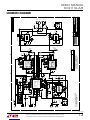
schematic Diagram
A
A
B
B
C
C
D
D
E
E
4
4
3
3
2
2
1
1
-B
4 PHASE HIGH CURRENT STEP-DOWN
CONVERTER WITH VERY LOW DCR INDUCTOR
IDEAL ORING DIODES
INPUT HOT SWAP CIRCUITS
FSW = 400kHz
-A
10V - 14V
-A
-B
NOTE: UNLESS OTHERWISE SPECIFIED
1. ALL RESISTORS ARE IN OHMS, 0603.
2. ALL CAPACITORS ARE 0603.
N+1 MOSFET FAILURE PROTECTION
-A: STUFFED ON -A ASSEMBLY ONLY
-B: STUFFED ON -B ASSEMBLY ONLY
HIGH EFFICIENCY CONVERTER
IOUT(MAX)
90A
120A
*
-B
-A
HIGH EFFICIENCY
HIGH EFFICIENCY
-A
-B
MODE
PS
BM
CCM
OPT, OPTIONAL: NOT STUFFED
ITH
VOS-
VOSNS
HIZB1
HIZB2
INTVCCA
5VBIAS1
ITH
5VBIAS2
VIN
5VBIAS2
VOUT1 VOUT
VIN
VOUT2
VIN2
ITEMP
TK/SS VOS+
VIN1
5VBIAS2
RUN
INTVCCA
CLKINA
HIZB2
ITEMP
VOUT1
VOS-
VOSNS
VIN2
5VBIAS1
5VBIAS1
5VBIAS2
TK/SS
INTVCCA
VOUT
ILIM
CLKOUTA
VOS-
HIZB1
VIN1
5VBIAS1
VOUT2
REV
REV
VOS+
/FLT1
/FLT2
VIN4
VIN1
VIN3
VIN2
VIN
RUN
HIZB1
HIZB2
RUN
INTVCCA
INTVCCA
SNSDC1+
SNSDC2+
SIZE
DATE:
IC NO. REV.
SHEET OF
TITLE:
APPROVALS
PCB DES.
APP ENG.
TECHNOLOGY Fax: (408)434-0507
Milpitas, CA 95035
Phone: (408)432-1900
1630 McCarthy Blvd.
LTC Confidential-For Customer Use Only
CUSTOMER NOTICE
LINEAR TECHNOLOGY HAS MADE A BEST EFFORT TO DESIGN A
CIRCUIT THAT MEETS CUSTOMER-SUPPLIED SPECIFICATIONS;
HOWEVER, IT REMAINS THE CUSTOMER'S RESPONSIBILITY TO
VERIFY PROPER AND RELIABLE OPERATION IN THE ACTUAL
APPLICATION. COMPONENT SUBSTITUTION AND PRINTED
CIRCUIT BOARD LAYOUT MAY SIGNIFICANTLY AFFECT CIRCUIT
PERFORMANCE OR RELIABILITY. CONTACT LINEAR
TECHNOLOGY APPLICATIONS ENGINEERING FOR ASSISTANCE.
THIS CIRCUIT IS PROPRIETARY TO LINEAR TECHNOLOGY AND
SCHEMATIC
SUPPLIED FOR USE WITH LINEAR TECHNOLOGY PARTS.
SCALE = NONE
www.linear.com
3
Wednesday, January 18, 2017
13
MS
N/A
LTC3774EUHE
LT
DC2111A
REVISION HISTORY
DESCRIPTION DATEAPPROVEDECO REV
MS
PRODUCTION3 01-18-17
__
REVISION HISTORY
DESCRIPTION DATEAPPROVEDECO REV
MS
PRODUCTION3 01-18-17
__
REVISION HISTORY
DESCRIPTION DATEAPPROVEDECO REV
MS
PRODUCTION3 01-18-17
__
R29
4.64K
1%
C2
0.22uF
R24
10
R9
10K
D7
CMHZ4683
12
E1
PGOOD
R184
100
R34
10
E11
VIN+
R46
10K
R37
30.1K
R26
OPT
+
COUT6
R3
1
R14
OPT
R10
0
E12
VIN-
RS1
0.007
2512
C10
4.7nF
J1
VOUT+
R15
0
D9
SMAJ17A
12
E3 VOS+
Q2
BSC010NE2LS
2
4
5
3
1
C1
2.2uF
16V
D6
1N4448HWT
R183
100
R52
10K
U2
LTC4352CDD
UV
3
GND
9
STATUS 5
OV
4
VIN 1
CPO 10
VCC
2
FAULT 6
OUT 8
REV
7
GATE 11
SOURCE 12
EP
13
D1
1N4448HWT
R54
0.000
2512
R31
0
R19
30.1K
Q4
FDMS86500DC
JP2
1
3
2
4
D2
1N4448HWT
R6
10K
R36
10K
J2 VOUT+
1.2V / *
C5
0.1uF
R2
56.2K
R55
0.000
2512
R28
0
R12
24.9K
C13
0.22uF
C23
100pF
Q1
BSC010NE2LS
2
4
5
3
1
RS2
0.007
2512
C3
OPT
0805
C15
4.7uF
10V
0805
C11
1uF
C12
0.22uF
TP7
C9
0.01uF
L1
0.33uH
744301033
WURTH EL.
R16
1.69K
J5 VOUT-
R48
0
R23
37.4K
R38
OPT
J7
VIN+
TP1
R49
OPT
R32
1
R153
0
R45
0
COUT2
TP5
TP2
JP1
ON
OFF
RUN
1
3
2
R41
38.3K
E5 VOS-
R112
0
R51
0.000
2512
J3
VOUT+
R64
10K
C22
OPT
+
COUT3
2.5V
C25
100pF
CIN3
R154
2K
1206
R21
0
R33
0
R18
4.64K
1%
+
COUT4
330uF
C16
0.22uF
+
COUT8
330uF
CIN1
+
COUT7
2.5V
R53
OPT
C31
0.1uF
TP6
U5
LTC4352CDD
UV
3
GND
9
STATUS 5
OV
4
VIN 1
CPO 10
VCC
2
FAULT 6
OUT 8
REV
7
GATE 11
SOURCE 12
EP
13
E2
TRACK/SS
R43
OPT
CIN2
22uF
25V
1210
R8
OPT
R5
10K
R47
0.000
2512
R39
2.4M
R25
OPT
R180
0
R1
100K
R22
10K
TP17
U4
FDMF5820DC
PWM 1
ZCD# 2
VCC 3
AGND 32
NC 6
PHASE 7
VIN 8
VIN
11
VIN
33
PGND
12
PGND
13
PGND
14
PGND
15
SW
16
SW
17
SW
18
SW
19
SW
20
SW
21
SW
22
EN/FAULT# 31
SW
23
SW 24
SW 25
SW 26
GL 27
PGND 28
PVCC 29
TMON 30
BOOT 5
GL 35
PGND
34
AGND 4
VIN
10
VIN
9
R17
10K
J8
VIN-
C18
2.2uF
16V
R30
2.2
R7
10K
U6
LTC4226CUD-1
VCC2
12
ON1
16
VCC1 1
SENSE1 2
GATE1 3
CLS
7
FAULT1 15
OUT1 4
FTMR1 5
FAULT2 14
OUT2
9
FTMR2 8
GND
6
GATE2
10
SENSE2
11
ON2
13
GND
17
L2
0.33uH
744301033
WURTH EL.
R13
0
C24
1uF
C7
OPT
+
CIN6
D8
1N4448HWT
R11
10K
J4 VOUT-
C4
47pF
D5
CMHZ4701
1 2
C19
0.22uF
+
COUT5
C6 2.2uF
16V
+
CIN7
150uF
25V
C17
1uF
R35
10K
U3
LTC3774EUHE
ITH2
2
VOSNS2-
3
VOSNS2+
4
TK/SS2
5
HIZB2
6
PWMEN2
7
PWM2
8
RUN2
9RUN1 20
PWM1 21
SNSDC1+ 18
TK/SS1 24
HIZB1 23
VOSNS1+ 25
VOSNS1- 26
ITH1 27
ILIM1
29
MODE/PLLIN
32
PWMEN1 22
SNSAC2+ 13
PGOOD2 14
PGOOD1 15
SNSAC1+ 16
SNS1- 17
PHMODE
30
FREQ
31
CLKOUT
33
INTVCC
34
VIN
35
ILIM2
36
ITEMP2
1
GND
10
ITEMP1 28
GND 19
SNS2- 12
SNSDC2+ 11
GND 37
R40
24.9K
J6 VOUT-
C14
0.22uF
COUT9
D18
1N4448HWT
D4
1N4448HWT
R50
0
C8
330pF
U1
FDMF5820DC
PWM 1
ZCD# 2
VCC 3
AGND 32
NC 6
PHASE 7
VIN 8
VIN
11
VIN
33
PGND
12
PGND
13
PGND
14
PGND
15
SW
16
SW
17
SW
18
SW
19
SW
20
SW
21
SW
22
EN/FAULT# 31
SW
23
SW 24
SW 25
SW 26
GL 27
PGND 28
PVCC 29
TMON 30
BOOT 5
GL 35
PGND
34
AGND 4
VIN
10
VIN
9
R42
0
R44
10K
COUT1
100uF
6.3V
1206
TP4
CIN5
25V
22uF
1210
R27
931
1%
COUT10
100uF
6.3V
1206
CIN4
22uF
25V
1210
C20 2.2uF
16V
R188 OPT
R4
0
E4
CLKINA
Q3
FDMS86500DC
D3
1N4448HWT
R189 OPT
C26
OPT
R20
931
1%
C21
0.1uF

14
dc2111aabf
DEMO MANUAL
DC2111A-A/-B
Linear Technology Corporation
1630 McCarthy Blvd., Milpitas, CA 95035-7417
(408) 432-1900 ● FAX: (408) 434-0507 ● www.linear.com
© LINEAR TECHNOLOGY CORPORATION 2017
LT 0217 • PRINTED IN USA
DEMONSTRATION BOARD IMPORTANT NOTICE
Linear Technology Corporation (LTC) provides the enclosed product(s) under the following AS IS conditions:
This demonstration board (DEMO BOARD) kit being sold or provided by Linear Technology is intended for use for ENGINEERING DEVELOPMENT
OR EVALUATION PURPOSES ONLY and is not provided by LTC for commercial use. As such, the DEMO BOARD herein may not be complete
in terms of required design-, marketing-, and/or manufacturing-related protective considerations, including but not limited to product safety
measures typically found in finished commercial goods. As a prototype, this product does not fall within the scope of the European Union
directive on electromagnetic compatibility and therefore may or may not meet the technical requirements of the directive, or other regulations.
If this evaluation kit does not meet the specifications recited in the DEMO BOARD manual the kit may be returned within 30 days from the date
of delivery for a full refund. THE FOREGOING WARRANTY IS THE EXCLUSIVE WARRANTY MADE BY THE SELLER TO BUYER AND IS IN LIEU
OF ALL OTHER WARRANTIES, EXPRESSED, IMPLIED, OR STATUTORY, INCLUDING ANY WARRANTY OF MERCHANTABILITY OR FITNESS
FOR ANY PARTICULAR PURPOSE. EXCEPT TO THE EXTENT OF THIS INDEMNITY, NEITHER PARTY SHALL BE LIABLE TO THE OTHER FOR
ANY INDIRECT, SPECIAL, INCIDENTAL, OR CONSEQUENTIAL DAMAGES.
The user assumes all responsibility and liability for proper and safe handling of the goods. Further, the user releases LTC from all claims
arising from the handling or use of the goods. Due to the open construction of the product, it is the user’s responsibility to take any and all
appropriate precautions with regard to electrostatic discharge. Also be aware that the products herein may not be regulatory compliant or
agency certified (FCC, UL, CE, etc.).
No License is granted under any patent right or other intellectual property whatsoever. LTC assumes no liability for applications assistance,
customer product design, software performance, or infringement of patents or any other intellectual property rights of any kind.
LTC currently services a variety of customers for products around the world, and therefore this transaction is not exclusive.
Please read the DEMO BOARD manual prior to handling the product. Persons handling this product must have electronics training and
observe good laboratory practice standards. Common sense is encouraged.
This notice contains important safety information about temperatures and voltages. For further safety concerns, please contact a LTC application
engineer.
Mailing Address:
Linear Technology
1630 McCarthy Blvd.
Milpitas, CA 95035
Copyright © 2004, Linear Technology Corporation
-
 1
1
-
 2
2
-
 3
3
-
 4
4
-
 5
5
-
 6
6
-
 7
7
-
 8
8
-
 9
9
-
 10
10
-
 11
11
-
 12
12
-
 13
13
-
 14
14


Linear Technology DC2111A-A/B Demo Manual
- Type
- Demo Manual
Ask a question and I''ll find the answer in the document
Finding information in a document is now easier with AI
Related papers
-
Linear Technology LTC3884EUK Demo Manual
-
-
-
-
-
-
-
-
-
Other documents
-
Analog Devices Linear DC2681A-A Demo Manual
-
Analog Devices DC2995A High Frequency, Step Down Supply, GaN FETs User manual
-
Linear DC1892A Demo Manual
-
Analog Devices LTC6952 Demo Manual
-
-
Texas Instruments bq500215 bqTESLA Wireless Power TX EVM (Rev. A) User guide
-
-
-
MICROCHIP EVB-USB5816 Operating instructions
-
Analog Devices LTM8080EY User manual