
Table of Contents
1
TABLE OF CONTENTS
1. INTRODUCTION
1.1. PREFACE.............................................................................................................1-1
1.2. KEY FEATURES..................................................................................................1-1
1.3. PERFORMANCE LIST.........................................................................................1-2
1.4. BLOCK DIAGRAM ...............................................................................................1-3
1.5. INTRODUCE THE Pentium II Processor..........................................................1-4
1.6. What is AGP?.......................................................................................................1-6
2. SPECIFICATION
2.1. HARDWARE........................................................................................................2-1
2.2. SOFTWARE.........................................................................................................2-2
2.3. ENVIRONMENT...................................................................................................2-2
3. HARDWARE INSTALLATION
3.1. UNPACKING........................................................................................................3-1
3.2. MAINBOARD LAYOUT........................................................................................3-1
3.3. QUICK REFERENCE FOR JUMPERS & CONNECTORS ................................3-2
3.4. DRAM INSTALLATION........................................................................................3-5
3.5. CPU SPEED SETUP ...........................................................................................3-6
3.6. CMOS RTC & ISA CFG CMOS SRAM................................................................3-7
3.7. SPEAKER CONNECTOR INSTALLATION ........................................................3-7
3.8. HARDWARE RESET SWITCH CONNECTOR INSTALLATION.......................3-7
3.9. POWER LED CONNECTOR INSTALLATION ...................................................3-7

6BXU
2
3.10. IDE & ATAPI DEVICE INSTALLATION.............................................................3-7
3.11. PERIPHERAL DEVICE INSTALLATION...........................................................3-7
3.12. KEYBOARD & PS/2 MOUSE INSTALLATION..................................................3-8
3.13. SCSI DEVICE INSTALLATION .........................................................................3-8
4. BIOS CONFIGURATION
4.1. ENTERING SETUP .............................................................................................4-1
4.2. CONTROL KEYS.................................................................................................4-1
4.3. GETTING HELP...................................................................................................4-2
4.3.1. Main Menu................................................................................................4-2
4.3.2. Status Page Setup Menu / Option Page Setup Menu...............................4-2
4.4. THE MAIN MENU.................................................................................................4-2
4.5. STANDARD CMOS SETUP MENU ....................................................................4-4
4.6. BIOS FEATURES SETUP...................................................................................4-8
4.7. CHIPSET FEATURES SETUP............................................................................4-13
4.8. POWER MANAGEMENT SETUP.......................................................................4-17
4.9. PNP/PCI CONFIGURATION...............................................................................4-21
4.10. LOAD BIOS DEFAULTS....................................................................................4-23
4.11. LOAD PERFORMANCE DEFAULTS................................................................4-24
4.12. INTEGRATED PERIPHERALS. ........................................................................4-25
4.13. SUPERVISOR PASSWORD/USER PASSWORD...........................................4-30
4.14. IDE HDD AUTO DETECTION...........................................................................4-31
4.15. SAVE & EXIT SETUP........................................................................................4-32
4.16. EXIT WITHOUT SAVING..................................................................................4-33

Introduction
1-1
1. INTRODUCTION
1.1. PREFACE
Welcome to use the 6BXU motherboard. It is a Pentium II Processor based
PC / AT compatible system with AGP / PCI / SCSI / ISA Bus, and has been
designed to be the fastest PC / AT system. There are some new features allow
you to operate the system with just the performance you want.
This manual also explains how to install the motherboard for operation, and
how to set up your CMOS CONFIGURATION with BIOS SETUP program.
1.2. KEY FEATURES
qIntel Pentium II Processor based PC / AT compatible mainboard.
qSlot 1 supports Pentium II processor running at 200-633 MHz.
qIntel 440BX chipset, Supports AGP / SDRAM / Ultra DMA/33 IDE / Wake on
LAN / Keyboard and PS/2 Mouse Power On / ACPI features.
qSupports Intel LDCM Network Manageability.
qSupports 4xDIMMs using 3.3V SDRAM DIMM module.
qSupports 8 MB - 1 GB SDRAM memory on board.
qSupports ECC or Non-ECC type DRAM module.
q1xAGP slot, 4xPCI Bus slots, 3xISA Bus slots.
qSupports 2 channels Ultra DMA/33 IDE ports for 4 IDE Devices.
qSupports both Ultra SCSI, Ultra Wide SCSI and Ultra II SCSI ports.
qSupports 2xCOM (16550), 1xLPT (EPP / ECP), 1x Floppy port.
qSupports 2xUSB ports, 1xPS/2 Mouse, 1xPS/2 Keyboard.
qLicensed AWARD BIOS, 2M bit FLASH RAM.
q30.5 cm x 21 cm ATX SIZE form factor, 4 layers PCB.

6BXU
1-2
1.3. PERFORMANCE LIST
The following performance data list is the testing results of some popular
benchmark testing programs.
These data are just referred by users, and there is no responsibility for different
testing data values gotten by users. (The different Hardware & Software
configuration will result in different benchmark testing results.)
•CPU Pentium II processor
•DRAM (32x4)MB SDRAM (SEC KM48S2020CT-G8)
•CACHE SIZE 512 KB included in CPU
•DISPLAY GA-601 AGP Display Card (4MB SGRAM)
•STORAGE Onboard Ultra Wide SCSI (IBM DRS-39130)
•O.S. Windows NT™ 4.0
•DRIVER Display Driver at 1024 x 768 x 256 colors x 75Hz.
Adaptec AIC-7890 SCSI Driver
Intel Pentium II
Processor 450MHz(100x4.5) 333MHz(66x5)
Winbench98
CPU mark32 1100 843
FPU Winmark 2290 1720
Business Disk 1930 1840
Hi-End Disk 4580 4460
Business Graphics 201 163
Hi-End Graphics 238 171
Winstone98Business 36 30.8
Hi-End 39.4 32.8

Introduction
1-3
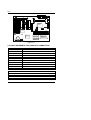
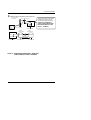
1.4. BLOCK DIAGRAM
48MHz
3.3V EDO/SDRAM
DIMM Sockets
14.318MHz
66 / 100
MHz
Ultra DMA/33
IDE Ports
IDE Bus
PCI Bus
ISA Bus
AGP Bus
LPT Port
Keyboard
Floppy Port
COM Ports
DRAM Bus
PS/2 Mouse
USB Bus
USB Ports
14.318MHz
48MHz
14.318MHz
I/O
CHIPSET
83977TF
SLOT1
Host Bus
INTEL
82443BX
CHIPSET
Clock Gen
Buffer
PIIX4
82371EB
CHIPSET
Clock Gen
AGP
66MHz
66/100
MHz
66/100
MHz
66/100MHz
33
MHz
PCI Bus
40MHz
OSC
SCSI
CHIPSET
AIC-7890P
Ultra SCSI Port
Ultra Wide SCSI
INT. LVD
EXT. LVD

6BXU
1-4
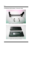
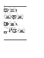
1.5. INTRODUCE THE Pentium
II Processor & AGP
Figure 1:Retention Mechanism & attach Mount
Figure 2:OEM Pentium II Processor

Introduction
1-5
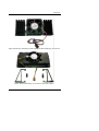
Figure 3:Heatsink / FAN & Heat sink support for OEM Pentium II Processor
Figure 4:Boxed Pentium II Processor & Heat sink support

6BXU
1-6
1.6 What is AGP
?
The Accelerated Graphics Port (AGP) is a new port on the Host-To-PCI bridge
device that supports an AGP port. The main purpose of the AGP port is to
provide fast access to system memory.
The AGP port can be used either as fast PCI port (32-bits at 66MHz vs. 32-bits
at 33MHz) or as an AGP port which supports 2x data-rate, a read queue, and
side band addressing. When the 2x-data rate is used the port can transmit data
at 533MB/sec (66.6*2*4). The read-queue can be used to pipeline reads –
removing the effects of the reads-latency. Side band addressing can be used to
transmit the data address on a separate line in order to speed up the
transaction.

Specification
2-1
2. SPECIFICATION
2.1. HARDWARE
• CPU − Pentium II processor 200 – 633 MHz.
− 242 pins 66/100MHz slot1 on board.
• PROTECTION − Speaker Alarm when detect "CPU FAN Failure" or
“CPU Overheat”.
− Automatically slow down CPU speed when "CPU
Overheat".
− Intel LDCM supported.
− H/W monitor power status (±5V, ±12V, 5V
SB,VGTL , CPU voltage & CMOS battery
voltage).(Optional)
• SPEED − 66/100 MHz system speed.
− 66 MHz AGP bus speed. (2X mode 133MHz)
− 33 MHz PCI-Bus speed.
− 8 MHz AT bus speed.
• DRAM MEMORY − 4 banks 168 pins DIMM module sockets on board.
− Use 8 / 16 / 32 / 64 / 128 / 256 MB DIMM module
DRAM.
− 8 ~ 1 GB SDRAM.
− Supports 3.3V SDRAM.
− Supports ECC or Non-ECC type DRAM.
• CACHE MEMORY − 32 KB 1st cache memory included in CPU.
− 256KB/512 KB 2nd cache in CPU.
− Supports DIB speed mode for L2 Cache.
• I/O BUS SLOTS − 4 33MHz Master / Slave PCI-BUS.
− 3 8MHz 16 bits ISA BUS.
− 1 66MHz / 133MHz AGP bus.
• IDE PORTS − 2 Ultra DMA/33 Bus Master IDE channels on
board.(Using IRQ14,15)

6BXU
2-2
− Support Mode 3,4 IDE & ATAPI CD – ROM.
• SCSI PORTS − Supports 1 Ultra Wide SCSI port.
− Supports 1 Ultra SCSI port.
− Supports 2 Ultra II SCSI port.
• I/O PORTS − Supports 2 16550 COM ports.
− Supports 1 EPP/ECP LPT port.
− Supports 1 Floppy port.
− Supports 2 USB ports.
− Supports PS/2 Mouse & Keyboard.
• GREEN FUNCTION − Suspend mode support.
− Green switch & ACPI LED support.
− IDE & Display power down support.
− Monitor all IRQ / DMA / Display / I/O events.
• BIOS − 2M bits FLASH RAM.
− Supports Plug & Play, DMI Function.
• DIMENSION − ATX Form Factor, 4 layers PCB.
2.2. SOFTWARE
• DRIVER − Intel LDCM (optional.)
− Health monitor Utility.
− Bus Master IDE Driver.
− Adaptec SCSI Driver.
• BIOS − Licensed AWARD BIOS.
− AT CMOS Setup, BIOS / Chipset Setup, Green
Setup, Hard Disk Utility included.
− Monitor Health status.
• O.S. − Operation with MS-DOS, Windows95,
WINDOWS NT, OS/2, NOVELL and SCO UNIX.
2.3. ENVIRONMENT
• Ambient Temp. − 0°C to +50°C (Operating).
• Relative Hum. − 0 to +85% (Operating).
• Altitude − 0 to 10,000 feet (Operating).
• Vibration − 0 to 1,000 Hz.

Specification
2-3
• Electricity − 4.9 V to 5.2 V. (Max. 20A current at 5V.)


Hardware Installation
3-1
3. HARDWARE INSTALLATION
3.1. UNPACKING
The mainboard package should contain the following:
•The 6BXU mainboard.
•The Retention Mechanism & Attach Mount
•USER'S MANUALS for mainboard & SCSI device.
•Cable set for IDE, Floppy, SCSI & I/O devices.
•Diskettes and CD for Mainboard Utility.
•External LVD port adapter.
The mainboard contains sensitive electric components, which can be easily
damaged by static electricity, so the mainboard should be left in its original
packing until it is installed.
Unpacking and installation should be done on a grounded anti-static mat. The
operator should be wearing an anti static wristband, grounded at the same
point as the anti-static mat.
Inspect the mainboard carton for obvious damage. Shipping and handling may
cause damage to your board. Be sure there are no shipping and handling
damages on the board before proceeding.
After opening the mainboard carton, extract the system board and place it only
on a grounded anti-static surface component side up. Again inspect the board
for damage. Press down on all of the socket IC's to make sure that they are
properly seated. Do this only on with the board placed on a firm flat surface.
M
DO NOT APPLY POWER TO THE BOARD IF IT HAS BEEN DAMAGED.
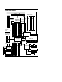
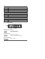
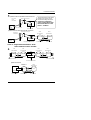
3.2. MAINBOARD LAYOUT

6BXU
3-2
6BXU
BIOS
INTEL
443BX
PIIX4
Adaptec
AIC-7890
Slot 1
SW
ATX Power
PS/2
USB
COMA COMB
LPT
JP1
CPU
FAN
JP5
BANK 0
BANK 1
BANK 2
BANK 3
DIMM 1
DIMM 2
DIMM 3
DIMM 4
IDE 1
IDE 2 FLOPPY
Ultra SCSI
Ultra Wide SCSI
Ultra II SCSI
BAT 1
JP10
IR
J13
AGP
PCI 1PCI 2PCI 3PCI 4
ISA 1ISA 2ISA 3
JP7
SB
-LINK
JP8
PWR
FAN
Panel
FAN
JP4
J14
×Figure 3.1Ø
3.3. QUICK REFERENCE FOR JUMPERS & CONNECTORS
t I/O Ports Connector
USB USB port.
Ultra SCSI Ultra SCSI port
Ultra Wide SCSI Ultra Wide SCSI port
Ultra II SCSI Ultra II SCSI port
IDE1 For Primary IDE port.
IDE2 For Secondary IDE port.
PS/2 For PS/2 Keyboard/Mouse port.
Floppy For Floppy port
COM B For Serial port2 (COM B).
COM A For Serial port1 (COM A).
LPT For LPT port.
t Slot 1
For Pentium II processor installed
tIR : INFRARED Connector (IR) -- Function Option
Pin No. Function

Hardware Installation
3-3
1IR Data Output
2GND
3IR Data Input
4Signal
5POWER (+)
t CPU FAN : CPU cooling FAN Power Connector
Pin No. Function
1GND.
2+12V
3SENSE
t PWR FAN : Power FAN Connector
Pin No. Function
1GND.
2+12V
3SENSE
t Panel FAN : Panel FAN Connector
Pin No. Function
1GND.
2+12V
3SENSE
t J13 : System Power On After Ac Back
Pin No. Function
1Signal
2GND
t JP1 : Keyboard Power On Selection
Pin No. Function
1-2 Enabled Keyboard Power On
2-3 Disabled Keyboard Power On
t JP7:SB-LINK For PCI Audio / Sound Card use only
Pin No. Function

6BXU
3-4
1Signal
2GND
3NC
4Signal
5GND
6Signal
t JP8 : Wake on LAN
Pin No. Function
1+5V SB
2GND
3Signal
t J14 : Case Open(Please remove shunted jumper before use.)
Pin No. Function
1Signal
2GND
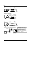
JP10 : 2*11 PIN Jumper
PW: Soft Power Connector
Open: Normal Operation
Short: Power On/Off
RE: Reset Switch Open: Normal Operation
Short: For Hardware Reset System
P+P-P-: Power LED
PIN 1 : anode (+)
PW P+P-P- H+
RE SPKR
GN
G−
JP10 1
1 1
1H−
G+GN
1

Hardware Installation
3-5
PIN 2 : cathode (−)
PIN 3 : cathode (−)
SPKR : Speaker Connector
PIN 1 : VCC
PIN 2 : NC
PIN 3 : NC
PIN 4 : Data
H
+
H
−
: IDE Hard Disk Active LED
PIN 1: LED anode (+)
PIN 2: LED cathode (−)
GN: Green Function Switch
Open : Normal operation
Short : Entering Green Mode
G
−
G
+
: Green LED
PIN 1 : LED anode (+)
PIN 2 : LED cathode (−)
3.4. DRAM INSTALLATION
The mainboard can be installed with 8 / 16 / 32 / 64 / 128 / 256 MB 168 pins
DIMM module DRAM, and the DRAM speed must be 50 or 60 ns for EDO &
67~100 MHz for SDRAM. The DRAM memory system on mainboard consists
of bank 0, 1, 2 & bank 3.
Since 168 pins DIMM module is 64 bits width, using 1 PCS which can match a
64 bits system. The total memory size is 8 MB ~ 1 GB EDO or SDRAM. The
DRAM installation position refer to Figure 3.1, and notice the Pin 1 of DIMM
module must match with the Pin 1 of DIMM socket. Insert the DRAM DIMM
module into the DIMM socket at Vertical angle. If there is a wrong direction of
Pin 1, the DRAM DIMM module couldn't be inserted into socket completely.
3.5. CPU SPEED SETUP
1
1
−
1+

6BXU
3-6
The system bus speed can be set to 66MHz or 100MHz form the jumper (JP5).
The user can change the DIP SWITCH (SW) selection to set up the CPU speed
for different processors. The CPU speed must match with the frequency
RATIO and Front Side Bus (FSB) speed. It will cause system hanging up if the
frequency RATIO and FSB Speed do not match with the CPU.
MJP5 (Select the system speed between 66 Hz and 100MHz)
1-2 Close Set system speed to 66MHz
−
system always
run at 66MHz FSB (Front Side Bus).
2-3 Close Set system speed to Auto
−
auto detect system
speed (66/ 100MHz FSB)
1-2-3 Open Set system speed to 100MHz
−
system always
run at 100MHz FSB (Front Side Bus).
DIP SWITCH (SW)
1 2 3 4
FREQ.
RATIO
EXT.CLK.
MHz
INT.CLK.
MHz CPU Type
OFF OFF ON ON 3.5 66 233 Pentium II 233 MHz
ON ON OFF ON 466 266 Pentium II 266 MHz
OFF ON OFF ON 4.5 66 300 Pentium II 300 MHz
ON OFF OFF ON 566 333 Pentium II 333 MHz
OFF OFF OFF ON 5.5 66 366 Pentium II 366 MHz
ON OFF ON ON 3100 300 Pentium II 300 MHz
OFF OFF ON ON 3.5 100 350 Pentium II 350 MHz
ON ON OFF ON 4100 400 Pentium II 400 MHz
OFF ON OFF ON 4.5 100 450 Pentium II 450 MHz
ON OFF OFF ON 5100 500 Pentium II 500 MHz
OFF OFF OFF ON 5.5 100 550 Pentium II 550 MHz
M
The CPU is a sensitive electric component and it can be easily
damaged by static electricity, so users must keep it away from metal
surface when the CPU is installed onto main board.
3.6. CMOS RTC & ISA CFG CMOS SRAM
1 2 3
1 2 3
1 2 3

Hardware Installation
3-7
There're RTC & CMOS SRAM on board; they have a power supply from
external battery to keep the DATA inviolate & effective. The RTC is a REAL-
TIME CLOCK device, which provides the DATE & TIME to system. The CMOS
SRAM is used for keeping the information of system configuration, so the
system can automatically boot OS every time. Since the lifetime of internal
battery is 5 years, the user can change a new Battery to replace old one after it
cannot work.
3.7. SPEAKER CONNECTOR INSTALLATION
There is a speaker in AT system for sound purpose. The 4 - Pins connector
SPKR is used to connect speaker. Anode connects +, Cathode connects −.
3.8. HARDWARE RESET SWITCH CONNECTOR INSTALLATION
The RESET switch on panel provides users with HARDWARE RESET function.
The system will do a cold start after the RESET switch is pushed and released
by user. The RESET switch is a 2 PIN connector and should be installed to RE
on mainboard.
3.9. POWER LED CONNECTOR INSTALLATION
System has power LED lamp on the panel of case. The power LED will light on
off or flash to indicate which step on the system. The connector should be
connected to PWR of mainboard in correct direction.
3.10. IDE & ATAPI DEVICE INSTALLATION
There are two-Enhanced PCI IDE ports (IDE1, IDE2) on board, which following
ATAPI standard SPEC. Any one IDE port can connected to two ATAPI devices
(IDE Hard Disk, CD-ROM & Tape Driver), so total four ATAPI devices can exist
in a system. The HD is the active LED port for ATAPI devices.
3.11. PERIPHERAL DEVICE INSTALLATION
After the I/O device installation and jumpers setup, the mainboard can be
mounted into the case and fixed by screw. To complete the mainboard
installation, the peripheral device could be installed now. The basic system
needs a display interface card. If the PCI - Bus device is to be installed in the
system, any one of four PCI - Bus slots can be used.
3.12. KEYBOARD & PS/2 MOUSE INSTALLATION

6BXU
3-8
The main board supports PS/2 Mouse (J1). The BIOS will auto detect whether
the PS/2 Mouse is installed or not & assign IRQ12 for PS/2 Mouse port if it is
installed. After installing the peripheral device, the user should check
everything again, and prepare to power-on the system.
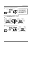
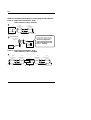
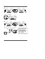
3.13. SCSI DEVICE INSTALLATION
There are four SCSI ports on board, One is 8bit SCSI port for ULTRA SCSI
device, the other one for Ultra wide SCSI , another is for Ultra II SCSI. And total
15 SCSI devices can exist in a system.
Single Ended and LVD Terminator Control are controlled by BIOS Setup (In the
INTEGRATED PERIPHERALS Setup page.)
Terminator ON/OFF rules
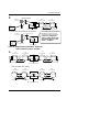
State 1. Ultra or Ultra wide SCSI Devices connecting to SE Port :
CASE 1: Single Ended Termination: Both
LVD Terminator Control : Enabled
1System has 16 bit SCSI
Mainboard
SCSI DEVICE
SCSI DEVICE
Terminator ON
Terminator OFF
Terminator ON
16 bit 16 bit
SE
15
System has only 8 bit SCSI device
Mainboard
Terminator ON
Terminator OFF
Terminator ON
SCSI DEVICE SCSI DEVICE
8 bit 8 bit
SE
7
2
Page is loading ...
Page is loading ...
Page is loading ...
Page is loading ...
Page is loading ...
Page is loading ...
Page is loading ...
Page is loading ...
Page is loading ...
Page is loading ...
Page is loading ...
Page is loading ...
-
 1
1
-
 2
2
-
 3
3
-
 4
4
-
 5
5
-
 6
6
-
 7
7
-
 8
8
-
 9
9
-
 10
10
-
 11
11
-
 12
12
-
 13
13
-
 14
14
-
 15
15
-
 16
16
-
 17
17
-
 18
18
-
 19
19
-
 20
20
-
 21
21
-
 22
22
-
 23
23
-
 24
24
-
 25
25
-
 26
26
-
 27
27
-
 28
28
-
 29
29
-
 30
30
-
 31
31
-
 32
32


