
R-01-01-080121
686DLX
USER'S MANUAL
Pentium
II Processor MAINBOARD
REV. 1 First Edition

686DLX
2
The author assumes no responsibility for any errors or omissions which may
appear in this document nor does it make a commitment to update the
information contained herein.
Third-party brands and names are the property of their respective
owners.
DECEMBER 06, 1997 Taipei, Taiwan

Table of Contents
3
TABLE OF CONTENTS
1. INTRODUCTION
1.1. PREFACE.............................................................................................................1-1
1.2. KEY FEATURES..................................................................................................1-1
1.3. PERFORMANCE LIST.........................................................................................1-2
1.4. BLOCK DIAGRAM ...............................................................................................1-3
1.5. INTRODUCE THE Pentium
II Processor & AGP..............................................1-4
1.6. What is AGP?.......................................................................................................1-6
1.7. What is RAID PORT?...........................................................................................1-6
2. SPECIFICATION
2.1. HARDWARE........................................................................................................2-1
2.2. SOFTWARE.........................................................................................................2-2
2.3. ENVIRONMENT...................................................................................................2-2
3. HARDWARE INSTALLATION
3.1. UNPACKING........................................................................................................3-1
3.2. MAINBOARD LAYOUT........................................................................................3-2
3.3. QUICK REFERENCE FOR JUMPERS & CONNECTORS ................................3-2
3.4. DRAM INSTALLATION........................................................................................3-5
3.5. CPU SPEED SETUP ...........................................................................................3-6
3.6. CMOS RTC & ISA CFG CMOS SRAM................................................................3-6
3.7. SPEAKER CONNECTOR INSTALLATION ........................................................3-7
3.8. HARDWARE RESET SWITCH CONNECTOR INSTALLATION.......................3-7
3.9. POWER LED CONNECTOR INSTALLATION ...................................................3-7

686DLX
4
3.10. IDE & ATAPI DEVICE INSTALLATION.............................................................3-7
3.11. SCSI DEVICE INSTALLATION .........................................................................3-8
3.12. PERIPHERAL DEVICE INSTALLATION...........................................................3-10
3.13. KEYBOARD & PS/2 MOUSE INSTALLATION..................................................3-10
3.14. KEYBOARD SETTING FUNCTION..................................................................3-10
4. BIOS CONFIGURATION
4.1. ENTERING SETUP .............................................................................................4-1
4.2. CONTROL KEYS.................................................................................................4-1
4.3. GETTING HELP...................................................................................................4-2
4.3.1. Main Menu........................................................................................................4-2
4.3.2. Status Page Setup Menu / Option Page Setup Menu.......................................4-2
4.4. THE MAIN MENU.................................................................................................4-2
4.5. STANDARD CMOS SETUP MENU ....................................................................4-4
4.6. BIOS FEATURES SETUP...................................................................................4-8
4.7. CHIPSET FEATURES SETUP............................................................................4-12
4.8. POWER MANAGEMENT SETUP.......................................................................4-17
4.9. PNP/PCI CONFIGURATION..............................................................................4-20
4.10. INTEGRATED PERIPHERALS .........................................................................4-23
4.11. LOAD SETUP DEFAULTS ................................................................................4-28
4.12. USER PASSWORD...........................................................................................4-29
4.13. IDE HDD AUTO DETECTION...........................................................................4-30
4.14. SAVE & EXIT SETUP........................................................................................4-31
4.15. EXIT WITHOUT SAVING..................................................................................4-32

Table of Contents
5


Introduction
1-1
1. INTRODUCTION
1.1. PREFACE
Welcome to use the 686DLX motherboard. The motherboard is a Dual
Pentium
II Processor based PC / AT compatible system with AGP / PCI /
ISA Bus, and has been designed to be the fastest PC / AT system. There are
some new features allow you to operate the system with just the performance
you want.
This manual also explains how to install the motherboard for operation, and
how to set up your CMOS CONFIGURATION with BIOS SETUP program.
1.2. KEY FEATURES
q Intel Dual Pentium
II Processor based PC / AT compatible mainboard.
q Dual Slot 1 on board supports dual Pentium
II processor running at 200-
633MHz.
q Intel 440LX chipset, Support AGP / SDRAM / Ultra DMA/33 IDE / ACPI
features.
q Support CPU FAN Failure / Overheat Alarm & auto slow down CPU
speed.
q Support Intel LDCM
Network Manageability.
q Supports 4xDIMMs using 3.3V EDO or SDRAM DIMM module.
q Supports 8 MB - 1 GB EDO / 512MB SDRAM memory on board.
q Supports ECC or Non-ECC type DRAM module.
q Supports Ultra & Ultra Wide SCSI ports for 15 SCSI Device.
q 1xAGP slot, 4xPCI Bus slots(1 PCI slot support RAID port), 3xISA Bus
slots.
q Supports 2 channels Ultra DMA/33 IDE ports for 4 IDE Device.
q Supports 2xCOM (16550), 1xLPT (EPP / ECP), 1x1.44MB Floppy port.
q Supports 2xUSB ports, 1xPS/2 Mouse & 1xPS/2 Keyboard ports.
q Licensed AWARD BIOS, 2M bit FLASH RAM.

686DLX
1-2
q ATX form factor, Double stack I/O connector, 4 layers PCB.
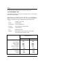
1.3. PERFORMANCE LIST
The following performance data list is the testing results of some popular
benchmark testing programs.
These data are just referred by users, and there is no responsibility for
different testing data values gotten by users. (The different Hardware &
Software configuration will result in different benchmark testing results.)
• CPU
Pentium
II processor
• DRAM 64 MB SDRAM
• CACHE SIZE 512 KB included in CPU
• DISPLAY Matrox Millennium II 4MB PCI VGA
• STORAGE Onboard IDE port
• O.S. Windows95 OSR2.0.
• DRIVER Display Driver at 1024 x 768 x 64K colors x 75Hz.
Triones Bus Master IDE Driver 3.60K
Intel Pentium
II
266MHz 300MHz
Winbench97
CPU mark32
697 783
Business Disk
2210 2260
Hi-End Disk
5890 6490
Business Graphic
116 127
Hi-End Graphic
50.8 56.3
Winstone 97
Business
62 64.9
Hi-End
30.6 32.6

Introduction
1-3
14.318MHz
66MHz
66MHz
8MHz
3.3V EDO/SDRAM
DIMM Sockets
Floppy Port
1.4. BLOCK DIAGRAM
SLOT1
14.318MHz
66MHz
24MHz
Ultra DMA/33
IDE Ports
IDE Bus
PCI Bus
66MHz
PCI Bus
33MHz
33MHz
33MHz
14.318MHz
48MHz
ISA Bus
AGP Bus
LPT Port
USB #2
PS/2 Keyboard
COM Ports
USB
DRAM
Bus
SLOT1
PS/2 Mouse
USB Bus
Host Bus
PAC
82443LX
CHIPSET
PIIX4
82371AB
CHIPSET
I/O
8661
CIPSET
KBC
8042
CLOCK
GEN
SC652EY
B
Adaptec
AIC-7880P
Ultra
Wide
SCSI
Ultra
SCSI
AGP
SLOT

686DLX
1-4
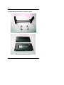
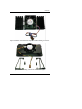
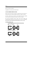
1.5. INTRODUCE THE Pentium
II Processor & AGP
Figure 1:Retention Mechanism & attach Mount
Figure 2:OEM Pentium
II Processor

Introduction
1-5
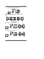
Figure 3:Heatsink / FAN & Heat sink support for OEM Pentium
II Processor
Figure 4:Boxed Pentium
II Processor & Heat sink support

686DLX
1-6
1.6. What is AGP
?
The Accelerated Graphics Port (AGP) is a new port on the Host-To-PCI
bridge device that supports an AGP port. The main purpose of the AGP port
is to provide fast access to system memory.
The AGP port can be used either as fast PCI port (32-bits at 66MHz vs. 32-
bits at 33MHz) or as an AGP port which supports 2x data-rate, a read queue,
and side band addressing. When the 2x-data rate is used the port can
transmit data at 533Mb/sec (66.6*2*4). The read-queue can be used to
pipeline reads – removing the effects of the reads-latency. Side band
addressing can be used to transmit the data address on a separate line in
order to further speed the transaction.
1.7. What is RAID PORT
?
RAID PORT is the most popular in netware server applications. For example,
it is having four Levels 0, 1, 0/1 and 5 (The RAID Levels is depend on your
RAID CARD) .
RAID 0 (two driver minimum) is achieved by creating an array of striped
disks. IF one driver in a RAID 0 system fails, all data on the array will be lost.
RAID 0 is typically not used in network applications.
RAID 1 (two drivers) is as disk mirroring or duplexing. It’ s read performance
is very good, because data can be read from either the primary or mirrored
disk. However, it’ s write performance is slignhtly slower than with singal disks,
because two requests must be issued to write the same data to both drivers.
RAID 0/1 (four driver minimunm) is as RAID 0+1, combines the performance
of data striping (RAID 0) with the fault tolerance of RAID1.
RAID 5 (three drivers minimum) strips blocks of data as well as parity data
across all driver in the array, ensuring that no data will be lost in the event of
a single driver failure. RAID 5 delivers improved performance by allowing
multiple, simultaneous read and write requests but it unlike the other RAID
levels.

Specification
2-1
2. SPECIFICATION
2.1. HARDWARE
• CPU − Dual Pentium
II processor 200 – 633 MHz.
− Dual 242 pins 66MHz slot1 on board.
• PROTECTION − Onboard Buzzer Alarm when detect "CPU FAN
Failure" or “CPU Overheat”.
− Automatically slow down CPU speed when "CPU
FAN Failure" or "CPU Overheat".
− Intel LDCM
support.
− H/W monitor power status (±5V, ±12V, CPU
voltage & CMOS battery voltage).
• SPEED − 66 MHz system speed.
− 66 MHz AGP bus speed. (133MHz 2*mode)
− 33 MHz PCI-Bus speed.
− 8 MHz AT bus speed.
• DRAM MEMORY − 4 banks 168 pins DIMM module sockets on board.
−
Use 8 / 16 / 32 / 64 / 128 / 256 MB 60~70 ns DIMM
module DRAM.
− 8 ~ 1 GB DRAM size.
− Support 3.3V SDRAM / EDO type DRAM.
− Support ECC or Non-ECC type DRAM.
• CACHE MEMORY − 32 KB 1st cache memory included in CPU.
− 256KB/512 KB 2nd cache in CPU.
− Support DIB speed mode for L2 Cache.
• SCSI PORTS
− Using Adaptec 7880P chipset.
− Supports one SCSI-2 or SCSI-3 (Ultra) port.
− Support one Ultra or Ultra Wide port.
− Support Adaptec RAID Port on board.
• I/O BUS SLOTS − 1 66 / 133MHz AGP BUS.
− 4 33MHz Master / Slave PCI-BUS.
− 3 8MHz 16 bits ISA BUS.
• IDE PORTS − 2 Ultra DMA/33 Bus Master IDE channels on
board.(Using IRQ14,15)
− Back ward Support Mode 3,4 IDE & ATAPI CD -
ROM.

686DLX
2-2
• I/O PORTS
− Supports 2 16550 COM ports. (Using IRQ4, 3)
− Supports 1 EPP/ECP LPT port. (Using IRQ7 or 5
and DMA3 or 1)
−
Supports 1 1.44/2.88 MB Floppy port. (Using DMA2
& IRQ6)
− Supports 2 USB ports.
− Supports PS/2 Mouse. (Using IRQ12 )
− Supports PS/2 Keyboard. (Using IRQ1 )
• GREEN FUNCTION − Suspend mode support.
− Green switch & LED support.
− IDE & Display power down support.
− Monitor all IRQ / DMA / Display / I/O events.
• BIOS − 256KB FLASH EEPROM.
− Supports Plug & Play, DMI, ACPI Function.
• DIMENSION − ATX Form Factor, 4 layers PCB.
2.2. SOFTWARE
• DRIVER − Intel LDCM
optional.
− Health monitor Utility.
− Bus Master IDE Driver.
− Suspend to HD Utility.
− ULTRA WIDE SCSI Driver .
• BIOS − Licensed AWARD BIOS.
− AT CMOS Setup, BIOS / Chipset Setup, Green
Setup, Hard Disk Utility included.
− Monitor Health status.
• O.S. − Operation with MS-DOS
, Windows
95,
WINDOWS NT, OS/2, NOVELL and SCO UNIX.
2.3. ENVIRONMENT
• Ambient Temp. − 0°C to +50°C (Operating).
• Relative Hum. − 0 to +85% (Operating).
• Altitude − 0 to 10,000 feet (Operating).
• Vibration − 0 to 1,000 Hz.
• Electricity − 4.9 V to 5.2 V.

Specification
2-3
− Max. 20A current at 5V.


Hardware Installation
3-1
3. HARDWARE INSTALLATION
3.1. UNPACKING
The mainboard package should contain the following:
• The 686DLX mainboard.
• The Retention Mechanism & Attach Mount
• USER'S MANUAL for mainboard.
• Cable set for IDE¡BFloppy & SCSI Device.
• Diskette & CD for SCSI Controller & Mainboard Utility.
The mainboard contains sensitive electric components, which can be easily
damaged by static electricity, so the mainboard should be left in its original
packing until it is installed.
Unpacking and installation should be done on a grounded anti-static mat.
The operator should be wearing an anti static wristband, grounded at the
same point as the anti-static mat.
Inspect the mainboard carton for obvious damage. Shipping and handling
may cause damage to your board. Be sure there are no shipping and
handling damages on the board before proceeding.
After opening the mainboard carton, extract the system board and place it
only on a grounded anti-static surface component side up. Again inspect the
board for damage. Press down on all of the socket IC's to make sure that
they are properly seated. Do this only on with the board placed on a firm flat
surface.
M
DO NOT APPLY POWER TO THE BOARD IF IT HAS BEEN DAMAGED.
You are now ready to install your mainboard. The mounting hole pattern on
the mainboard matches the ATX system board. It is assumed that the
chassis is designed for a standard ATX mainboard mounting.
Place the chassis on the anti-static mat and remove the cover. Take the clips,
stand-off and screws for mounting the system board, and keep them

686DLX
3-2
separate.
3.2. MAINBOARD LAYOUT
SLOT4
PCI1
PCI2
PCI3
COMA
COMB
LPT
USB
KB
Mouse
ATX
POWER
S1
BIOS
RESET
HD-LED GN-SW
CN9
IDE1
CN8
FLOPP
CN1
CN3
CN2
CN5
CN4
J2
DIMM1
DIMM2
DIMM3
DIMM4
Bank 1
Bank 0
FAN
BUZZER
J1
AGP
BAT1
SLOT2
RAID PORT
686DLX
JP2
Bank 3
Bank 2
J5 J6
J7
J8 J9 J10 J11
IR
PWR-ON
SPEAKER
PWR-LED
CN10
IDE2
1
2
3
4
J4
J3
HT2
FAN
SLOT6
CN6
CN7
J12
GN-LED
PCI4
PIIX
371A
Adapte
AIC-7880P
JP5
J13
SLOT5
SLOT3
SLOT1
×Figure 3.1Ø
3.3. QUICK REFERENCE FOR JUMPERS & CONNECTORS
t CN1-10 I/O Ports Connector
CN1 For Serial port1 (COM A).
CN2 For LPT port.
CN3 For Serial port2 (COM B).
CN4 For PS/2 Mouse & Keyboard I/O ports.
CN5 For USB port.
CN6 For ULTRA 8 bit SCSI port.
CN7 For ULTRA WIDE SCSI port.
CN8 For Floppy port.
CN9 For Primary IDE port.
CN10 For Secondary IDE port.

Hardware Installation
3-3
t J1: slot1 (For CPU2)
For Pentium
II processor installed.
t J2: CPU2 cooling FAN Power Connector
Pin No. Function
1 GND.
2 +12V
3 SENSE
t J3: slot1 (For CPU1)
For Pentium
II processor installed.
t J4: CPU1 cooling FAN Power Connector
Pin No. Function
1 GND.
2 +12V
3 SENSE
t J5: SPEAKER Connector
Pin No. Function
1 VCC
2 NC.
3 NC.
4 Output
t J6: RESET Switch
Pin No. Function
1 RESET Input
2 GND
t J7: POWER ON LED (PW-LED)
Pin No. Function
1 LED POWER (+)
2 NC

686DLX
3-4
3 GND (-)
t J8: Hard Disk active LED (HD-LED)
Pin No. Function
1 LED POWER (+)
2 LED POWER (-)
3 NC
4 LED POWER (+)
t J9: INFRARED Connector (IR) -- Function Option
Pin No. Function
1 IR Data Output
2 GND
3 IR Data Input
4 NC
5 POWER (+)
t J10: GN-SW
On – Off for enter suspend Green Mode.
t J11: Soft Power Switch
On – Off for POWER ON or Suspend IN / OUT.
On 4 sec. For POWER OFF before VGA Enable or CMOS setup select
“delay 4sec.” For POWER OFF mode.
t J12: Green LED
OFF Normal mode
ON Suspend mode
t J16: Wake on Lan
Pin No. Function
1 +5V SB.
2 GND.
3 Signal.
t JP5: ATX POWER USE only
Pin No. Function
ON System After AC BACK: Full_ON.
OFF System After AC BACK: Soft_OFF.
Page is loading ...
Page is loading ...
Page is loading ...
Page is loading ...
Page is loading ...
Page is loading ...
Page is loading ...
Page is loading ...
-
 1
1
-
 2
2
-
 3
3
-
 4
4
-
 5
5
-
 6
6
-
 7
7
-
 8
8
-
 9
9
-
 10
10
-
 11
11
-
 12
12
-
 13
13
-
 14
14
-
 15
15
-
 16
16
-
 17
17
-
 18
18
-
 19
19
-
 20
20
-
 21
21
-
 22
22
-
 23
23
-
 24
24
-
 25
25
-
 26
26
-
 27
27
-
 28
28


