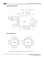
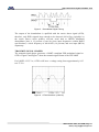
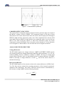
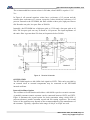
Microcyber HT1200M is a single-chip, half-duplex 1200 bits per second FSK modem designed for use in Highway Addressable Remote Transducer (HART) field instruments and masters. The HT1200M uses Phase Continuous Frequency Shift Keying (FSK) at 1200 bits per second and provides all of the functions needed to satisfy HART physical layer requirements including modulation, demodulation, receive filtering, carrier detect, and transmit-signal shaping.
Key Features:
- Can be used in designs presently using the SYM20C15 or equivalent type chip
- 3.3V-5.0V power supply
- Transmit-signal wave shaping


-
 1
1
-
 2
2
-
 3
3
-
 4
4
-
 5
5
-
 6
6
-
 7
7
-
 8
8
-
 9
9
-
 10
10
-
 11
11
-
 12
12
-
 13
13
-
 14
14
-
 15
15
-
 16
16
-
 17
17
-
 18
18
-
 19
19


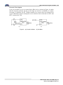
Microcyber HT1200M is a single-chip, half-duplex 1200 bits per second FSK modem designed for use in Highway Addressable Remote Transducer (HART) field instruments and masters. The HT1200M uses Phase Continuous Frequency Shift Keying (FSK) at 1200 bits per second and provides all of the functions needed to satisfy HART physical layer requirements including modulation, demodulation, receive filtering, carrier detect, and transmit-signal shaping.
Key Features:
- Can be used in designs presently using the SYM20C15 or equivalent type chip
- 3.3V-5.0V power supply
- Transmit-signal wave shaping
Ask a question and I''ll find the answer in the document
Finding information in a document is now easier with AI
Other documents
-
DeLOCK 83049 Datasheet
-
Texas Instruments Respiration Rate Measurement Using Impedance Pneumography Application notes
-
 Cypress CY8C24423A User manual
-
 Remote Automation Solutions Bristol Highway Addressable Remote Transducer (HART) Device Interface Owner's manual
-
NXP MC12311 Reference guide
-
 Cypress CapSense CY8C20x66 User manual
-
 Cypress CY8C24094 User manual
-
Rosemount 2081-CT Conductivity Microprocessor Transmitter Owner's manual
-
Cypress CY3274 User manual
-
 Cypress CY8C21234 User manual


