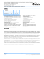
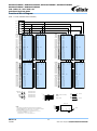
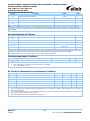
CnMemory 2GB SO-DIMM, DDR2, PC2-6400 User manual
- Category
- Memory modules
- Type
- User manual

M2N1G64TUH8D4F / M2N2G64TU8HD4B / M2N1G64TUH8D5F / M2N2G64TU8HD5B
M2N1G64TUH8D6F / M2N2G64TU8HD6B
1GB: 128M x 64 / 2GB: 256M x 64
Unbuffered DDR2 SO-DIMM
REV 1.1 1
07/2008
© NANYA TECHNOLOGY CORPORATION
NANYA reserves the right to change products and specifications without notice.
Based on DDR2-667/800 64Mx16 (1GB)/128Mx8 (2GB) SDRAM D-Die
Features
• Performance:
Speed Sort
PC2-5300
PC2-6400
Unit
-3C
-AC
DIMM CAS Latency
5
5
fck – Clock Freqency
333
400
MHz
tck – Clock Cycle
3
2.5
ns
Data Transfer Speed
667
800
Mbps
• 200-Pin Small Outline Dual In-Line Memory Module (SO-DIMM)
• 1GB: 128Mx64 Unbuffered DDR2 SO-DIMM based on 64Mx16
DDR2 SDRAM D Die devices
• 2GB: 256Mx64 Unbuffered DDR2 SO-DIMM based on 128Mx8
DDR2 SDRAM D Die devices
• Intended for 333MHz and 400MHz applications
• Inputs and outputs are SSTL-18 compatible
• V
DD
= V
DDQ
= 1.8V ±0.1V
• SDRAMs have 8 internal banks for concurrent operation
• Differential clock inputs
• Data is read or written on both clock edges
• DRAM DLL aligns DQ and DQS transitions with clock transitions
• Address and control signals are fully synchronous to positive
clock edge
• Auto Refresh (CBR) and Self Refresh Modes
• Automatic and controlled precharge commands
• Programmable Operation:
- DIMM Latency: 3, 4, 5
- Burst Type: Sequential or Interleave
- Burst Length: 4, 8
- Operation: Burst Read and Write
• 13/10/2 Addressing (1GB)
• 14/10/2 Addressing (2GB)
• 7.8 s Max. Average Periodic Refresh Interval
• Serial Presence Detect
• Gold contacts
• 1GB module’s SDRAMs are 84-ball BGA Package
• 2GB module’s SDRAMs are 60-ball BGA Package
• RoHS compliance
Description
M2N1G64TUH8D4F, M2N2G64TU8HD4B, M2N1G64TUH8D5F, M2N2G64TU8HD5B, M2N1G64TUH8D6F and M2N2G64TU8HD6B are
unbuffered 200-Pin Double Data Rate 2 (DDR2) Synchronous DRAM Small Outline Dual In-Line Memory Module (SO-DIMM), organized as
two ranks of 128Mx64 (1GB)/256Mx64 (2GB) high-speed memory array. M2N1G64TUH8D4F, M2N1G64TUH8D5F and 2N1G64TUH8D6F
use eight 64Mx16 84-ball BGA packaged devices and M2N2G64TU8HD4B, M2N2G64TU8HD5B and M2N2G64TU8HD6B use sixteen
128Mx8 60-ball BGA packaged devices. These DIMMs are manufactured using raw cards developed for broad industry use as reference
designs. The use of these common design files minimizes electrical variation between suppliers. All Elixir DDR2 SODIMMs provide a
high-performance, flexible 8-byte interface in a space-saving footprint.
The DIMM is intended for use in applications operating of 333MHz/400MHz clock speeds and achieves high-speed data transfer speed of
667Mbps/800Mbps. Prior to any access operation, the device latency and burst/length/operation type must be programmed into the
DIMM by address inputs A0-A12 (1GB) / A0-A13 (2GB) and I/O inputs BA0, BA1 and BA2 using the mode register set cycle.
The DIMM uses serial presence-detect implemented via a serial EEPROM using a standard IIC protocol. The first 128 bytes of SPD data are
programmed and locked during module assembly. The remaining 128 bytes are available for use by the customer.

M2N1G64TUH8D4F / M2N2G64TU8HD4B / M2N1G64TUH8D5F / M2N2G64TU8HD5B
M2N1G64TUH8D6F / M2N2G64TU8HD6B
1GB: 128M x 64 / 2GB: 256M x 64
Unbuffered DDR2 SO-DIMM
REV 1.1 2
07/2008
© NANYA TECHNOLOGY CORPORATION
NANYA reserves the right to change products and specifications without notice.
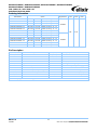
Ordering Information
Part Number
Speed
Organization
Power
Leads
Note
M2N2G64TU8HD4B –AC
DDR2-800
PC2-6400
400MHz (2.50ns @ CL = 5)
256Mx64
1.8V
Gold
M2N2G64TU8HD4B –3C
DDR2-667
PC2-5300
333MHz (3.00ns @ CL = 5)
M2N2G64TU8HD5B –AC
DDR2-800
PC2-6400
400MHz (2.50ns @ CL = 5)
M2N2G64TU8HD5B –3C
DDR2-667
PC2-5300
333MHz (3.00ns @ CL = 5)
M2N2G64TU8HD6B –AC
DDR2-800
PC2-6400
400MHz (2.50ns @ CL = 5)
M2N2G64TU8HD6B –3C
DDR2-667
PC2-5300
333MHz (3.00ns @ CL = 5)
M2N1G64TUH8D4F –AC
DDR2-800
PC2-6400
400MHz (2.50ns @ CL = 5)
128Mx64
M2N1G64TUH8D4F –3C
DDR2-667
PC2-5300
333MHz (3.00ns @ CL = 5)
M2N1G64TUH8D5F –AC
DDR2-800
PC2-6400
400MHz (2.50ns @ CL = 5)
M2N1G64TUH8D5F –3C
DDR2-667
PC2-5300
333MHz (3.00ns @ CL = 5)
M2N1G64TUH8D6F –AC
DDR2-800
PC2-6400
400MHz (2.50ns @ CL = 5)
M2N1G64TUH8D6F –3C
DDR2-667
PC2-5300
333MHz (3.00ns @ CL = 5)
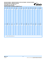
Pin Description
CK0, CK1, ,
Differential Clock Inputs
DQ0-DQ63
Data input/output
CKE0, CKE1
Clock Enable
DQS0-DQS7
Bidirectional data strobes
Row Address Strobe
-
Differential data strobes
Column Address Strobe
DM0-DM7
Input Data Masks
Write Enable
V
DD
Power (1.8V)
,
Chip Selects
V
REF
Ref. Voltage for SSTL_18 inputs
A0-A9 A11-A13
Row Address Inputs
V
DDSPD
Serial EEPROM positive power supply
A0-A9
Column Address Inputs
V
SS
Ground
A10/AP
Column Address Input/Auto-precharge
SCL
Serial Presence Detect Clock Input
BA0, BA1, BA2
SDRAM Bank Address Inputs
SDA
Serial Presence Detect Data input/output
ODT0, ODT1
Active termination control lines
SA0, SA1
Serial Presence Detect Address Inputs
NC
No Connect
Note: A13 is only support in 2GB module type.

M2N1G64TUH8D4F / M2N2G64TU8HD4B / M2N1G64TUH8D5F / M2N2G64TU8HD5B
M2N1G64TUH8D6F / M2N2G64TU8HD6B
1GB: 128M x 64 / 2GB: 256M x 64
Unbuffered DDR2 SO-DIMM
REV 1.1 3
07/2008
© NANYA TECHNOLOGY CORPORATION
NANYA reserves the right to change products and specifications without notice.
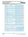
1GB/2GB DDR2 SDRAM SODIMM Pinout
Pin
Front
Pin
Back
Pin
Front
Pin
Back
Pin
Front
Pin
Back
Pin
Front
Pin
Back
1
V
REF
2
V
SS
51
DQS2
52
DM2
101
A1
102
A0
151
DQ42
152
DQ46
3
V
SS
4
DQ4
53
V
SS
54
V
SS
103
V
DD
104
V
DD
153
DQ43
154
DQ47
5
DQ0
6
DQ5
55
DQ18
56
DQ22
105
A10/AP
106
BA1
155
V
SS
156
V
SS
7
DQ1
8
V
SS
57
DQ19
58
DQ23
107
BA0
108
157
DQ48
158
DQ52
9
V
SS
10
DM0
59
V
SS
60
V
SS
109
110
159
DQ49
160
DQ53
11
12
V
SS
61
DQ24
62
DQ28
111
V
DD
112
V
DD
161
V
SS
162
V
SS
13
DQS0
14
DQ6
63
DQ25
64
DQ29
113
114
ODT0
163
NC
164
CK1
15
V
SS
16
DQ7
65
V
SS
66
V
SS
115
116
A13/NC
165
V
SS
166
17
DQ2
18
V
SS
67
DM3
68
117
V
DD
118
V
DD
167
168
V
SS
19
DQ3
20
DQ12
69
NC
70
DQS3
119
ODT1
120
NC
169
DQS6
170
DM6
21
V
SS
22
DQ13
71
V
SS
72
V
SS
121
V
SS
122
V
SS
171
V
SS
172
V
SS
23
DQ8
24
V
SS
73
DQ26
74
DQ30
123
DQ32
124
DQ36
173
DQ50
174
DQ54
25
DQ9
26
DM1
75
DQ27
76
DQ31
125
DQ33
126
DQ37
175
DQ51
176
DQ55
27
V
SS
28
V
SS
77
V
SS
78
V
SS
127
V
SS
128
V
SS
177
V
SS
178
V
SS
29
30
CK0
79
CKE0
80
CKE1
129
130
DM4
179
DQ56
180
DQ60
31
DQS1
32
81
V
DD
82
V
DD
131
DQS4
132
V
SS
181
DQ57
182
DQ61
33
V
SS
34
V
SS
83
NC
84
NC
133
V
SS
134
DQ38
183
V
SS
184
V
SS
35
DQ10
36
DQ14
85
BA2
86
NC
135
DQ34
136
DQ39
185
DM7
186
37
DQ11
38
DQ15
87
V
DD
88
V
DD
137
DQ35
138
V
SS
187
V
SS
188
DQS7
39
V
SS
40
V
SS
89
A12
90
A11
139
V
SS
140
DQ44
189
DQ58
190
V
SS
41
V
SS
42
V
SS
91
A9
92
A7
141
DQ40
142
DQ45
191
DQ59
192
DQ62
43
DQ16
44
DQ20
93
A8
94
A6
143
DQ41
144
V
SS
193
V
SS
194
DQ63
45
DQ17
46
DQ21
95
V
DD
96
V
DD
145
V
SS
146
195
SDA
196
V
SS
47
V
SS
48
V
SS
97
A5
98
A4
147
DM5
148
DQS5
197
SCL
198
SA0
49
50
NC
99
A3
100
A2
149
V
SS
150
V
SS
199
V
DDSPD
200
SA1
Note: 1. All pin assignments are consistent for all 8-byte unbuffered versions.
2. A13 is for 2GB modules only.

M2N1G64TUH8D4F / M2N2G64TU8HD4B / M2N1G64TUH8D5F / M2N2G64TU8HD5B
M2N1G64TUH8D6F / M2N2G64TU8HD6B
1GB: 128M x 64 / 2GB: 256M x 64
Unbuffered DDR2 SO-DIMM
REV 1.1 4
07/2008
© NANYA TECHNOLOGY CORPORATION
NANYA reserves the right to change products and specifications without notice.
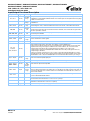
Input/Output Functional Description
Symbol
Type
Polarity
Function
CK0, CK1
(SSTL)
Positive
Edge
The positive line of the differential pair of system clock inputs which drives the input to the
on-DIMM PLL. All the DDR2 SDRAM address and control inputs are sampled on the rising edge
of their associated clocks.
,
(SSTL)
Negative
Edge
The negative line of the differential pair of system clock inputs which drives the input to the
on-DIMM PLL.
CKE0, CKE1
(SSTL)
Active
High
Activates the SDRAM CK signal when high and deactivates the CK signal when low. By
deactivating the clocks, CKE low initiates the Power Down mode, or the Self Refresh mode.
,
(SSTL)
Active
Low
Enables the associated SDRAM command decoder when low and disables the command
decoder when high. When the command decoder is disabled, new commands are ignored but
previous operations continue.
, ,
(SSTL)
Active
Low
When sampled at the positive rising edge of the clock, , , define the operation to be
executed by the SDRAM.
V
REF
Supply
Reference voltage for SSTL-18 inputs
ODT0, ODT1
Input
Active
High
On-Die Termination control signals
BA0, BA1, BA2
(SSTL)
-
Selects which SDRAM bank is to be active.
A0 – A9
A10/AP
A11, A12/A13
(SSTL)
-
During a Bank Activate command cycle, A0-A12/A13 define the row address (RA0-RA12/RA13)
when sampled at the rising clock edge. A13 applies on 2GB SODIMM only.
During a Read or Write command cycle, A0-A9 defines the column address (CA0-CA9) when
sampled at the rising clock edge. In addition to the column address, AP is used to invoke
Autoprecharge operation at the end of the Burst Read or Write cycle. If AP is high,
autoprecharge is selected and BA0/BA1/BA2 define the bank to be precharged. If AP is low,
autoprecharge is disabled.
During a Precharge command cycle, AP is used in conjunction with BA0/BA1/BA2 to control
which bank(s) to precharge. If AP is high all 8 banks will be precharged regardless of the state of
BA0/BA1/BA2. If AP is low, then BA0/BA1/BA2 are used to define which bank to pre-charge.
DQ0 – DQ63
(SSTL)
Active
High
Data and Check Bit Input/Output pins.
V
DD
, V
SS
Supply
Power and ground for the DDR2 SDRAM input buffers and core logic
DQS0 – DQS7
–
(SSTL)
Negative
and
Positive
Edge
Data strobe for input and output data
DM0 – DM7
Input
Active
High
The data write masks, associated with one data byte. In Write mode, DM operates as a byte
mask by allowing input data to be written if it is low but blocks the write operation if it is high. In
Read mode, DM lines have no effect. DM8 is associated with check bits CB0-CB7, and is not
used on x64 modules.
SA0 – SA1
-
Address inputs. Connected to either VDD or VSS on the system board to configure the Serial
Presence Detect EEPROM address.
SDA
-
This bi-directional pin is used to transfer data into or out of the SPD EEPROM. A resistor must be
connected from the SDA bus line to V DD to act as a pull-up.
SCL
-
This signal is used to clock data into and out of the SPD EEPROM. A resistor may be connected
from the SCL bus time to V DD to act as a pull-up.
V
DDSPD
Supply
Serial EEPROM positive power supply.

M2N1G64TUH8D4F / M2N2G64TU8HD4B / M2N1G64TUH8D5F / M2N2G64TU8HD5B
M2N1G64TUH8D6F / M2N2G64TU8HD6B
1GB: 128M x 64 / 2GB: 256M x 64
Unbuffered DDR2 SO-DIMM
REV 1.1 5
07/2008
© NANYA TECHNOLOGY CORPORATION
NANYA reserves the right to change products and specifications without notice.
Functional Block Diagram
[1GB – 2 Ranks, 64Mx16 DDR2 SDRAMs]
V
DDSPD
V
SS
SPD
V
DD
V
REF
V
DDID
Notes :
1. DQ wiring may differ from that described in this drawing.
2. DQ/DQS/DM/CKE/S S relationships are maintained as shown.
3. DQ/DQS/DM/DQS resistors are 22 +/- 5% Ohms
4. V
DDID
strap connections (for memory device V
DD
, V
DDQ
):
STRAP OUT (OPEN): V
DD
= V
DDQ
STRAP IN
(
V
SS
):
V
DD
is not equal to V
DDQ
4 loads
CK0
CK1
4 loads
Serial PD
A0 A2A1
SCL
WP
SDA
SA0 SA1
DQ48
DQ49
DQ50
DQ55
DQ52
DQ54
DQ53
DQ51
DQ56
DQ57
DQ58
DQ63
DQ60
DQ62
DQ61
DQ59
DQS6
DM6
DQS7
DM7
DM4
DQS4
DQ32
DQ33
DQ34
DQ39
DQ36
DQ38
DQ37
DQ35
DQ40
DQ41
DQ42
DQ47
DQ44
DQ46
DQ45
DQ43
DQS5
DM5
DM0
DQ0
DQ1
DQ2
DQ7
DQ4
DQ6
DQ5
DQ3
DQ8
DQ9
DQ10
DQ15
DQ12
DQ14
DQ13
DQ11
DQS0
DM1
DQS1
I/O 0
I/O 1
I/O 6
I/O 5
I/O 4
I/O 3
I/O 2
I/O 7
LDM
D0
I/O 8
I/O 9
I/O 14
I/O 13
I/O 12
I/O 11
I/O 10
I/O 15
UDM
UDQS
LDQS
DM3
DM2
DQS2
DQ16
DQ17
DQ18
DQ23
DQ20
DQ22
DQ21
DQ19
DQ24
DQ25
DQ26
DQ31
DQ28
DQ30
DQ29
DQ27
DQS3
ODT1
ODT0
CKE1
CKE0
C
K
E
O
D
T
3 Ohms +/- 5%
BA0-BA2
A0-A12
SDRAMS D0-D7
SDRAMS D0-D7
SDRAMS D0-D7
SDRAMS D0-D7
SDRAMS D0-D7
SA0
SA1
D0-D7, VDD and VDDQ
D0-D7
D0-D7, SPD
I/O 0
I/O 1
I/O 6
I/O 5
I/O 4
I/O 3
I/O 2
I/O 7
LDM
D4
I/O 8
I/O 9
I/O 14
I/O 13
I/O 12
I/O 11
I/O 10
I/O 15
UDM
UDQS
LDQS
C
K
E
O
D
T
I/O 0
I/O 1
I/O 6
I/O 5
I/O 4
I/O 3
I/O 2
I/O 7
LDM
D1
I/O 8
I/O 9
I/O 14
I/O 13
I/O 12
I/O 11
I/O 10
I/O 15
UDM
UDQS
LDQS
C
K
E
O
D
T
I/O 0
I/O 1
I/O 6
I/O 5
I/O 4
I/O 3
I/O 2
I/O 7
LDM
D5
I/O 8
I/O 9
I/O 14
I/O 13
I/O 12
I/O 11
I/O 10
I/O 15
UDM
UDQS
LDQS
C
K
E
O
D
T
I/O 0
I/O 1
I/O 6
I/O 5
I/O 4
I/O 3
I/O 2
I/O 7
LDM
D2
I/O 8
I/O 9
I/O 14
I/O 13
I/O 12
I/O 11
I/O 10
I/O 15
UDM
UDQS
LDQS
C
K
E
O
D
T
I/O 0
I/O 1
I/O 6
I/O 5
I/O 4
I/O 3
I/O 2
I/O 7
LDM
D3
I/O 8
I/O 9
I/O 14
I/O 13
I/O 12
I/O 11
I/O 10
I/O 15
UDM
UDQS
LDQS
C
K
E
O
D
T
I/O 0
I/O 1
I/O 6
I/O 5
I/O 4
I/O 3
I/O 2
I/O 7
LDM
D6
I/O 8
I/O 9
I/O 14
I/O 13
I/O 12
I/O 11
I/O 10
I/O 15
UDM
UDQS
LDQS
C
K
E
O
D
T
I/O 0
I/O 1
I/O 6
I/O 5
I/O 4
I/O 3
I/O 2
I/O 7
LDM
D7
I/O 8
I/O 9
I/O 14
I/O 13
I/O 12
I/O 11
I/O 10
I/O 15
UDM
UDQS
LDQS
C
K
E
O
D
T

M2N1G64TUH8D4F / M2N2G64TU8HD4B / M2N1G64TUH8D5F / M2N2G64TU8HD5B
M2N1G64TUH8D6F / M2N2G64TU8HD6B
1GB: 128M x 64 / 2GB: 256M x 64
Unbuffered DDR2 SO-DIMM
REV 1.1 6
07/2008
© NANYA TECHNOLOGY CORPORATION
NANYA reserves the right to change products and specifications without notice.
Functional Block Diagram
[2GB – 2 Ranks, 128M x8 DDR2 SDRAMs]
Notes :
Unless otherwise noted resistor values are 22 Ohms +/- 5%
DQ wiring may differ from that described in this drawing.
However, DQ/DM/DQS/DQS relationships are maintained as shown.
Serial PD
A0
A2
A1
SCL
WP
SDA
CS0
CS1
ODT1
ODT0
CKE1
CKE0
3 Ohms +/- 5%
SA0
SA1
SCL
V
DDSPD
V
SS
Serial PD
SDRAMS D0-D15, VDD and VDDQ
V
DD
V
REF
SDRAMS D0-D15
SDRAMS D0-D15 and SPD
BA0-BA2
A0-A13
RAS
SDRAMS D0-D15
WE
CAS
10 Ohms +/- 5%
DM0
DQ0
DQ1
DQ2
DQ7
DQ4
DQ6
DQ5
DQ3
DQS0
DQS0
I/O 0
I/O 1
I/O 6
I/O 5
I/O 4
I/O 3
I/O 2
I/O 7
DM
CS0
D0
DQS
DQS CKE0 ODT0
DM1
DQ8
DQ9
DQ10
DQ15
DQ12
DQ14
DQ13
DQ11
DQS1
DQS1
I/O 0
I/O 1
I/O 6
I/O 5
I/O 4
I/O 3
I/O 2
I/O 7
D1
DM2
DQ16
DQ17
DQ18
DQ23
DQ20
DQ22
DQ21
DQ19
DQS2
DQS2
I/O 0
I/O 1
I/O 6
I/O 5
I/O 4
I/O 3
I/O 2
I/O 7
D10
DM3
DQ24
DQ25
DQ26
DQ31
DQ28
DQ30
DQ29
DQ27
DQS3
DQS3
I/O 0
I/O 1
I/O 6
I/O 5
I/O 4
I/O 3
I/O 2
I/O 7
D11
DM4
DQ32
DQ33
DQ34
DQ39
DQ36
DQ38
DQ37
DQ35
DQS4
DQS4
I/O 0
I/O 1
I/O 6
I/O 5
I/O 4
I/O 3
I/O 2
I/O 7
D4
DM5
DQ40
DQ41
DQ42
DQ47
DQ44
DQ46
DQ45
DQ43
DQS5
DQS5
I/O 0
I/O 1
I/O 6
I/O 5
I/O 4
I/O 3
I/O 2
I/O 7
D5
DM6
DQ48
DQ49
DQ50
DQ55
DQ52
DQ54
DQ53
DQ51
DQS6
DQS6
I/O 0
I/O 1
I/O 6
I/O 5
I/O 4
I/O 3
I/O 2
I/O 7
D14
DM7
DQ56
DQ57
DQ58
DQ63
DQ60
DQ62
DQ61
DQ59
DQS7
DQS7
I/O 0
I/O 1
I/O 6
I/O 5
I/O 4
I/O 3
I/O 2
I/O 7
D15
8 loads
CK0
CK0
5.6pF
8 loads
CK1
5.6pF
CK1
SDRAMS D0-D15
SDRAMS D0-D15
SDRAMS D0-D15
SDRAMS D0-D15
DM
CS0
DQS
DQS CKE0 ODT0
DM
CS0
DQS
DQS CKE0 ODT0
DM
CS0
DQS
DQS CKE0 ODT0
DM
CS0
DQS
DQS CKE0 ODT0
DM
CS0
DQS
DQS CKE0 ODT0
DM
CS0
DQS
DQS CKE0 ODT0
DM
CS0
DQS
DQS CKE0 ODT0
I/O 0
I/O 1
I/O 6
I/O 5
I/O 4
I/O 3
I/O 2
I/O 7
DM
CS1
D8
DQS
DQS CKE1 ODT1
I/O 0
I/O 1
I/O 6
I/O 5
I/O 4
I/O 3
I/O 2
I/O 7
DM
CS1
D9
DQS
DQS CKE1 ODT1
I/O 0
I/O 1
I/O 6
I/O 5
I/O 4
I/O 3
I/O 2
I/O 7
DM
CS1
D2
DQS
DQS CKE1 ODT1
I/O 0
I/O 1
I/O 6
I/O 5
I/O 4
I/O 3
I/O 2
I/O 7
DM
CS1
D3
DQS
DQS CKE1 ODT1
I/O 0
I/O 1
I/O 6
I/O 5
I/O 4
I/O 3
I/O 2
I/O 7
DM
CS1
D12
DQS
DQS CKE1 ODT1
I/O 0
I/O 1
I/O 6
I/O 5
I/O 4
I/O 3
I/O 2
I/O 7
DM
CS1
D13
DQS
DQS CKE1 ODT1
I/O 0
I/O 1
I/O 6
I/O 5
I/O 4
I/O 3
I/O 2
I/O 7
DM
CS1
D6
DQS
DQS CKE1 ODT1
I/O 0
I/O 1
I/O 6
I/O 5
I/O 4
I/O 3
I/O 2
I/O 7
DM
CS1
D7
DQS
DQS CKE1 ODT1

M2N1G64TUH8D4F / M2N2G64TU8HD4B / M2N1G64TUH8D5F / M2N2G64TU8HD5B
M2N1G64TUH8D6F / M2N2G64TU8HD6B
1GB: 128M x 64 / 2GB: 256M x 64
Unbuffered DDR2 SO-DIMM
REV 1.1 7
07/2008
© NANYA TECHNOLOGY CORPORATION
NANYA reserves the right to change products and specifications without notice.
Serial Presence Detect (1GB – 2 Ranks, 64Mx16 DDR2 SDRAMs) (Part 1 of 2)
Byte
Description
SPD Entry Value
Serial PD Data Entry (Hex.)
Note
-3C
-AC
-3C
-AC
0
Number of Serial PD Bytes Written during Production
128
80
80
1
Total Number of Bytes in Serial PD device
256
08
08
2
Fundamental Memory Type
DDR2 SDRAM
08
08
3
Number of Row Addresses on Assembly
13
0D
0D
4
Number of Column Addresses on Assembly
10
0A
0A
5
Number of DIMM Ranks, Package, and Height
Module Height = 30.0mm, 2 ranks
61
61
6
Data Width of Assembly
X64
40
40
7
Reserved
Undefined
00
00
8
Voltage Interface Level of this Assembly
SSTL 1.8V
05
05
9
DDR2 SDRAM Device Cycle Time at CL=5
3ns
2.5ns
30
25
10
DDR2 SDRAM Device Access Time (t
ac
) from Clock
at CL=5
0.45ns
0.4ns
45
40
11
DIMM Configuration Type
Non Address/Command Parity,
Non Data ECC,
Non Data Parity,
00
00
12
Refresh Rate/Type
7.8 μs
82
82
13
Primary DDR2 SDRAM Width
X16
10
10
14
Error Checking DDR2 SDRAM Device Width
Undefined
00
00
15
Reserved
Undefined
00
00
16
DDR2 SDRAM Device Attributes: Burst Length
Supported
4,8
0C
0C
17
DDR2 SDRAM Device Attributes: Number of Device
Banks
8
08
08
18
DDR2 SDRAM Device Attributes: Latencies
Supported
3,4,5
38
38
19
DIMM Mechanical Characteristics
x ≤ 3.80 (mm)
01
01
20
DDR2 SDRAM DIMM Type Information
SO-DIMM (67.6mm)
04
04
21
DDR2 SDRAM Module Attributes
Analysis probe installed : No,
FET Switch External Enable : No,
Number of PLLs : 0,
Number of Active Registers : 1,
00
00
22
DDR2 SDRAM Device Attributes: General
Supports Weak Driver,
Supports 50 ohm ODT,
Supports PASR,
07
07
23
Minimum Clock Cycle at CL=4
3.75ns
3D
3D
24
Maximum Data Access Time from Clock at CL=4
0.5ns
50
50
25
Minimum Clock Cycle Time at CL=3
5ns
50
50
26
Maximum Data Access Time from Clock at CL=3
0.6ns
60
60
27
Minimum Row Precharge Time (t
RP
)
15ns
12.5ns
3C
32
28
Minimum Row Active to Row Active delay (t
RRD
)
10ns
28
28
29
Minimum to delay (t
RCD
)
15ns
12.5ns
3C
32
30
Minimum Active to Precharge Time (t
RAS
)
45ns
2D
2D
31
Module Rank Density
512MB
80
80
32
Address and Command Setup Time Before Clock
(t
IS
)
0.2ns
0.17ns
20
17
33
Address and Command Hold Time After Clock (t
IH
)
0.27ns
0.25ns
27
25
34
Data Input Setup Time Before Clock (t
DS
)
0.1ns
0.05ns
10
05
35
Data Input Hold Time After Clock (tDH)
0.17ns
0.12ns
17
12
36
Write Recovery Time (t
WR
)
15ns
3C
3C

M2N1G64TUH8D4F / M2N2G64TU8HD4B / M2N1G64TUH8D5F / M2N2G64TU8HD5B
M2N1G64TUH8D6F / M2N2G64TU8HD6B
1GB: 128M x 64 / 2GB: 256M x 64
Unbuffered DDR2 SO-DIMM
REV 1.1 8
07/2008
© NANYA TECHNOLOGY CORPORATION
NANYA reserves the right to change products and specifications without notice.
Serial Presence Detect (1GB – 2 Ranks, 64Mx16 DDR2 SDRAMs) (Part 2 of 2)
Byte
Description
SPD Entry Value
Serial PD Data Entry (Hex.)
Note
-3C
-AC
-3C
-AC
37
Internal Write to Read Command delay (t
WTR
)
7.5ns
1E
1E
38
Internal Read to Precharge delay (t
RTP
)
7.5ns
1E
1E
39
Reserved
Undefined
00
00
40
Extension of Byte 41 t
RC
and Byte 42 t
RFC
The number below a decimal point of
tRC and tRFC are 0, tRFC is less than
256ns.
06
36
41
Minimum Core Cycle Time (t
RC
)
60ns
57.5ns
3C
39
42
Min. Auto Refresh Command Cycle Time (t
RFC
)
127.5ns
7F
7F
43
Maximum Clock Cycle Time (t
CK
)
8ns
80
80
44
Max. DQS-DQ Skew Factor (tQHS)
0.24ns
0.2ns
18
14
45
Read Data Hold Skew Factor (tQHS)
0.34ns
0.3ns
22
1E
46-61
Reserved
Undefined
00
00
62
SPD Reversion
1.3
13
13
63
Checksum for Byte 0-62
Checksum Data
AA
90
64-71
Manufacturer’s JEDEC ID Code
Nanya
7F7F7F0B00000000
72
Module Manufacturing Location
Manufacturing code
-
73-91
Module Part number
Module Part Number in ASCII
-
1
92-255
Reserved
Undefined
-
Note 1:
Module part number:
M2N1G64TUH8D4F-3C4D324E31473634545548384434462D33432020
M2N1G64TUH8D4F-AC4D324E31473634545548384434462D41432020
M2N1G64TUH8D5F-3C4D324E31473634545548384435462D33432020
M2N1G64TUH8D5F-AC4D324E31473634545548384435462D41432020
M2N1G64TUH8D6F-3C4D324E31473634545548384436462D33432020
M2N1G64TUH8D6F-AC4D324E31473634545548384436462D41432020

M2N1G64TUH8D4F / M2N2G64TU8HD4B / M2N1G64TUH8D5F / M2N2G64TU8HD5B
M2N1G64TUH8D6F / M2N2G64TU8HD6B
1GB: 128M x 64 / 2GB: 256M x 64
Unbuffered DDR2 SO-DIMM
REV 1.1 9
07/2008
© NANYA TECHNOLOGY CORPORATION
NANYA reserves the right to change products and specifications without notice.
Serial Presence Detect (2GB – 2 Ranks, 128Mx8 DDR2 SDRAMs) (Part 1 of 2)
Byte
Description
SPD Entry Value
Serial PD Data Entry (Hex.)
Note
-3C
-AC
-3C
-AC
0
Number of Serial PD Bytes Written during Production
128
80
80
1
Total Number of Bytes in Serial PD device
256
08
08
2
Fundamental Memory Type
DDR2 SDRAM
08
08
3
Number of Row Addresses on Assembly
14
0E
0E
4
Number of Column Addresses on Assembly
10
0A
0A
5
Number of DIMM Ranks, Package, and Height
Module Height = 30.0mm, 2 ranks
61
61
6
Data Width of Assembly
X64
40
40
7
Reserved
Undefined
00
00
8
Voltage Interface Level of this Assembly
SSTL 1.8V
05
05
9
DDR2 SDRAM Device Cycle Time at CL=5
3ns
2.5ns
30
25
10
DDR2 SDRAM Device Access Time (t
ac
) from Clock
at CL=5
0.45ns
0.4ns
45
40
11
DIMM Configuration Type
Non Address/Command Parity,
Non Data ECC,
Non Data Parity,
00
00
12
Refresh Rate/Type
7.8 μs
82
82
13
Primary DDR2 SDRAM Width
X8
08
08
14
Error Checking DDR2 SDRAM Device Width
Undefined
00
00
15
Reserved
Undefined
00
00
16
DDR2 SDRAM Device Attributes: Burst Length
Supported
4,8
0C
0C
17
DDR2 SDRAM Device Attributes: Number of Device
Banks
8
08
08
18
DDR2 SDRAM Device Attributes: Latencies
Supported
3,4,5
38
38
19
DIMM Mechanical Characteristics
x ≤ 3.80 (mm)
01
01
20
DDR2 SDRAM DIMM Type Information
SO-DIMM (67.6mm)
04
04
21
DDR2 SDRAM Module Attributes
Analysis probe installed : No,
FET Switch External Enable : No,
Number of PLLs : 0,
Number of Active Registers : 1,
00
00
22
DDR2 SDRAM Device Attributes: General
Supports Weak Driver,
Supports 50 ohm ODT,
Supports PASR,
07
07
23
Minimum Clock Cycle at CL=4
3.75ns
3D
3D
24
Maximum Data Access Time from Clock at CL=4
0.5ns
50
50
25
Minimum Clock Cycle Time at CL=3
5ns
50
50
26
Maximum Data Access Time from Clock at CL=3
0.6ns
60
60
27
Minimum Row Precharge Time (t
RP
)
15ns
12.5ns
3C
32
28
Minimum Row Active to Row Active delay (t
RRD
)
7.5ns
1E
1E
29
Minimum to delay (t
RCD
)
15ns
12.5ns
3C
32
30
Minimum Active to Precharge Time (t
RAS
)
45ns
2D
2D
31
Module Rank Density
1GB
01
01
32
Address and Command Setup Time Before Clock
(t
IS
)
0.2ns
0.17ns
20
17
33
Address and Command Hold Time After Clock (t
IH
)
0.27ns
0.25ns
27
25
34
Data Input Setup Time Before Clock (t
DS
)
0.1ns
0.05ns
10
05
35
Data Input Hold Time After Clock (tDH)
0.17ns
0.12ns
17
12
36
Write Recovery Time (t
WR
)
15ns
3C
3C

M2N1G64TUH8D4F / M2N2G64TU8HD4B / M2N1G64TUH8D5F / M2N2G64TU8HD5B
M2N1G64TUH8D6F / M2N2G64TU8HD6B
1GB: 128M x 64 / 2GB: 256M x 64
Unbuffered DDR2 SO-DIMM
REV 1.1 10
07/2008
© NANYA TECHNOLOGY CORPORATION
NANYA reserves the right to change products and specifications without notice.
Serial Presence Detect (2GB – 2 Ranks, 128 M x 8 DDR2 SDRAMs) (Part 2 of 2)
Byte
Description
SPD Entry Value
Serial PD Data Entry (Hex.)
Note
-3C
-AC
-3C
-AC
37
Internal Write to Read Command delay (t
WTR
)
7.5ns
1E
1E
38
Internal Read to Precharge delay (t
RTP
)
7.5ns
1E
1E
39
Reserved
Undefined
00
00
40
Extension of Byte 41 t
RC
and Byte 42 t
RFC
The number below a decimal point of
tRC and tRFC are 0, tRFC is less than
256ns.
06
36
41
Minimum Core Cycle Time (t
RC
)
60ns
57.5ns
3C
39
42
Min. Auto Refresh Command Cycle Time (t
RFC
)
127.5ns
7F
7F
43
Maximum Clock Cycle Time (t
CK
)
8ns
80
80
44
Max. DQS-DQ Skew Factor (tQHS)
0.24ns
0.2ns
18
14
45
Read Data Hold Skew Factor (tQHS)
0.34ns
0.3ns
22
1E
46-61
Reserved
Undefined
00
00
62
SPD Reversion
1.3
13
13
63
Checksum for Byte 0-62
Checksum Data
1A
00
64-71
Manufacturer’s JEDEC ID Code
Nanya
7F7F7F0B00000000
72
Module Manufacturing Location
Manufacturing code
-
73-91
Module Part number
Module Part Number in ASCII
-
1
92-255
Reserved
Undefined
-
Note 1:
Module part number:
M2N2G64TU8HD4B-3C4D324E32473634545538484434422D33432020
M2N2G64TU8HD4B-AC4D324E32473634545538484434422D41432020
M2N2G64TU8HD5B-3C4D324E32473634545538484435422D33432020
M2N2G64TU8HD5B-AC4D324E32473634545538484435422D41432020
M2N2G64TU8HD6B-3C4D324E32473634545538484436422D33432020
M2N2G64TU8HD6B-AC4D324E32473634545538484436422D41432020

M2N1G64TUH8D4F / M2N2G64TU8HD4B / M2N1G64TUH8D5F / M2N2G64TU8HD5B
M2N1G64TUH8D6F / M2N2G64TU8HD6B
1GB: 128M x 64 / 2GB: 256M x 64
Unbuffered DDR2 SO-DIMM
REV 1.1 11
07/2008
© NANYA TECHNOLOGY CORPORATION
NANYA reserves the right to change products and specifications without notice.
Environmental Requirements
Symbol
Parameter
Rating
Units
T
OPR
Operating Temperature (ambient)
0 to 65
°C
H
OPR
Operating Humidity (relative)
10 to 90
%
T
STG
Storage Temperature
-50 to 100
°C
H
STG
Storage Humidity (without condensation)
5 to 95
%
Barometric pressure (operating & storage) up to 9850ft.
105 to 69
kPa
Note: Stress greater than those listed may cause permanent damage to the device. This is a stress rating only and device functional
operation at or above the conditions indicated is not implied. Exposure to absolute maximum rating conditions for extended periods may
affect reliability
Absolute Maximum DC Ratings
Symbol
Parameter
Rating
Units
V
DD
Voltage on VDD pins relative to Vss
-1.0 to +2.3
V
V
DDQ
Voltage on VDDQ pins relative to Vss
-0.5 to +2.3
V
V
DDL
Voltage on VDDL pins relative to Vss
-0.5 to +2.3
V
V
IN
, V
OUT
Voltage on I/O pins relative to Vss
-0.5 to +2.3
V
T
STG
Storage Temperature (Plastic)
-55 to +100
°C
Note: Stresses greater than those listed under “Absolute Maximum Ratings” may cause permanent damage to the device. This is stress
rating only, and functional operation of the device at these or any other conditions above those indicated in the operational sections of this
specification is not implied. Exposure to absolute maximum rating conditions for extended periods may affect reliability.
Storage temperature is the case surface temperature on the center/top side of the DRAM.
Operating temperature Conditions
Symbol
Parameter
Rating
Units
Note
T
CASE
Operating Temperature (Ambient)
0 to 95
°C
1
Note:
1. Case temperature is measured at top and center side of any DRAMs.
2. t
CASE
> 85°C t
REFI
= 3.9 μs
DC Electrical Characteristics and Operating Conditions
Symbol
Parameter
Min
Max
Units
Notes
VDD
Supply Voltage
1.7
1.9
V
1
VDDL
DLL Supply Voltage
1.7
1.9
V
1
VDDQ
Output Supply Voltage
1.7
1.9
V
1
VSS, VSSQ
Supply Voltage, I/O Supply Voltage
0
0
V
VREF
Input Reference Voltage
0.49VDDQ
0.51VDDQ
V
1, 2
VTT
Termination Voltage
VREF – 0.04
VREF + 0.04
V
3
Note:
1. There is no specific device VDD supply voltage requirement for SSTL_18 compliance. However, VDDQ must be less than or equal to
VDD under all conditions.
2. VREF is expected to be equal to 0.5 V DDQ of the transmitting device, and to track variations in the DC level of the same. Peak-to-peak
noise on VREF may not exceed 2% of the DC value.
3. VTT of transmitting device must track VREF of receiving device.

M2N1G64TUH8D4F / M2N2G64TU8HD4B / M2N1G64TUH8D5F / M2N2G64TU8HD5B
M2N1G64TUH8D6F / M2N2G64TU8HD6B
1GB: 128M x 64 / 2GB: 256M x 64
Unbuffered DDR2 SO-DIMM
REV 1.1 12
07/2008
© NANYA TECHNOLOGY CORPORATION
NANYA reserves the right to change products and specifications without notice.
ODT DC Electrical Characteristics
Parameter/Condition
Symbol
Min.
Nom.
Max.
Units
Note
Rtt effective impedance value for EMRS(A6,A2)=0,1; 75ohm
Rtt1(eff)
60
75
90
ohm
1
Rtt effective impedance value for EMRS(A6,A2)=1,0; 150ohm
Rtt2(eff)
120
150
180
ohm
1
Rtt effective impedance value for EMRS(A6,A2)=1,1; 50ohm
Rtt3(eff)
40
50
60
ohm
1
Deviation of V
M
with respect to VDDQ/2
Delta VM
-6
+6
%
1
Note1: Test condition for Rtt measurements.
Input AC/DC logic level
Symbol
Parameter
PC2-5300
PC2-6400
Units
Min.
Max.
Min.
Max.
VIH (AC)
Input High (Logic1) Voltage
VREF +
0.200
-
VREF +
0.200
-
V
VIL (AC)
Input Low (Logic0) Voltage
-
VREF –
0.200
-
VREF –
0.200
V
VIH (DC)
Input High (Logic1) Voltage
VREF +
0.125
VDDQ + 0.3
VREF +
0.125
VDDQ + 0.3
V
VIL (DC)
Input Low (Logic0) Voltage
-0.3
VREF –
0.125
-0.3
VREF –
0.125
V

M2N1G64TUH8D4F / M2N2G64TU8HD4B / M2N1G64TUH8D5F / M2N2G64TU8HD5B
M2N1G64TUH8D6F / M2N2G64TU8HD6B
1GB: 128M x 64 / 2GB: 256M x 64
Unbuffered DDR2 SO-DIMM
REV 1.1 13
07/2008
© NANYA TECHNOLOGY CORPORATION
NANYA reserves the right to change products and specifications without notice.
Operating, Standby, and Refresh Currents
T
CASE
= 0 °C ~ 85 °C; V
DDQ
= V
DD
= 1.8V ± 0.1V [1GB, 2 Ranks, 64Mx16 DDR2 SDRAMs]
Symbol
Parameter/Condition
PC2-5300
(-3C)
PC2-6400
(-AC)
Unit
IDD0
Operating Current: one bank; active/precharge; t
RC
= t
RC (MIN)
; t
CK
= t
CK (MIN)
;
DQ, DM, and DQS inputs changing twice per clock cycle; address and
control inputs changing once per clock cycle
693
782
mA
IDD1
Operating Current: one bank; active/read/precharge; Burst = 4; t
RC
= t
RC
(MIN)
; CL= 4; t
CK
= t
CK (MIN)
; I
OUT
= 0mA; address and control inputs changing
once per clock cycle
796
900
mA
IDD2P
Precharge Power-Down Standby Current: all banks idle; power-down
mode; CKE V
IL (MAX)
; t
CK
= t
CK (MIN)
88
88
mA
IDD2Q
Precharge quiet standby current
379
412
mA
IDD2N
Idle Standby Current: CS V
IH (MIN)
; all banks idle; CKE V
IH (MIN)
; t
CK
= t
CK
(MIN)
; address and control inputs changing once per clock cycle
549
620
mA
IDD3PF
Active Power-Down Standby Current: one bank active; power-down
mode; CKE V
IL (MAX)
; t
CK
= t
CK (MIN)
; MRS(12)=0
250
265
mA
IDD3PS
Active Power-Down Standby Current: one bank active; power-down
mode; CKE V
IL (MAX)
; t
CK
= t
CK (MIN)
; MRS(12)=1
106
106
mA
IDD3N
Active Standby Current: one bank; active/precharge; CS V
IH (MIN)
; CKE
V
IH (MIN)
; t
RC
= t
RAS (MAX)
; t
CK
= t
CK (MIN)
; DQ, DM, and DQS inputs changing
twice per clock cycle; address and control inputs changing once per clock
cycle
510
561
mA
IDD4R
Operating Current: one bank; Burst = 4; reads; continuous burst; address
and control inputs changing once per clock cycle; DQ and DQS outputs
changing twice per clock cycle; CL = 4; t
CK
= t
CK (MIN)
; I
OUT
= 0mA
928
1032
mA
IDD4W
Operating Current: one bank; Burst = 4; writes; continuous burst; address
and control inputs changing once per clock cycle; DQ and DQS inputs
changing twice per clock cycle; CL= 4; t
CK
= t
CK (MIN)
804
886
mA
IDD5B
Burst Refresh Current: t
RC
= t
RFC (MIN)
1223
1270
mA
IDD6
Self-Refresh Current: CKE 0.2V
97
97
mA
IDD7
Operating Current: four bank; four bank interleaving with BL = 4, address
and control inputs randomly changing; 50% of data changing at every
transfer; t
RC
= t
RC (min)
; I
OUT
= 0mA.
1751
1952
mA
Note: Module IDD was calculated from component IDD. It may differ from the actual measurement.

M2N1G64TUH8D4F / M2N2G64TU8HD4B / M2N1G64TUH8D5F / M2N2G64TU8HD5B
M2N1G64TUH8D6F / M2N2G64TU8HD6B
1GB: 128M x 64 / 2GB: 256M x 64
Unbuffered DDR2 SO-DIMM
REV 1.1 14
07/2008
© NANYA TECHNOLOGY CORPORATION
NANYA reserves the right to change products and specifications without notice.
Operating, Standby, and Refresh Currents
T
CASE
= 0 °C ~ 85 °C; V
DDQ
= V
DD
= 1.8V ± 0.1V [2GB, 2 Ranks, 128M x 8 DDR2 SDRAMs]
Symbol
Parameter/Condition
PC2-5300
(-3C)
PC2-6400
(-AC)
Unit
IDD0
Operating Current: one bank; active/precharge; t
RC
= t
RC (MIN)
; t
CK
= t
CK (MIN)
;
DQ, DM, and DQS inputs changing twice per clock cycle; address and
control inputs changing once per clock cycle
1379
1556
mA
IDD1
Operating Current: one bank; active/read/precharge; Burst = 4; t
RC
= t
RC
(MIN)
; CL= 4; t
CK
= t
CK (MIN)
; I
OUT
= 0mA; address and control inputs changing
once per clock cycle
1293
1447
mA
IDD2P
Precharge Power-Down Standby Current: all banks idle; power-down
mode; CKE V
IL (MAX)
; t
CK
= t
CK (MIN)
176
176
mA
IDD2Q
Precharge quiet standby current
771
840
mA
IDD2N
Idle Standby Current: CS V
IH (MIN)
; all banks idle; CKE V
IH (MIN)
; t
CK
= t
CK
(MIN)
; address and control inputs changing once per clock cycle
1115
1252
mA
IDD3PF
Active Power-Down Standby Current: one bank active; power-down
mode; CKE V
IL (MAX)
; t
CK
= t
CK (MIN)
; MRS(12)=0
524
553
mA
IDD3PS
Active Power-Down Standby Current: one bank active; power-down
mode; CKE V
IL (MAX)
; t
CK
= t
CK (MIN)
; MRS(12)=1
231
234
mA
IDD3N
Active Standby Current: one bank; active/precharge; CS V
IH (MIN)
; CKE
V
IH (MIN)
; t
RC
= t
RAS (MAX)
; t
CK
= t
CK (MIN)
; DQ, DM, and DQS inputs changing
twice per clock cycle; address and control inputs changing once per clock
cycle
989
1086
mA
IDD4R
Operating Current: one bank; Burst = 4; reads; continuous burst; address
and control inputs changing once per clock cycle; DQ and DQS outputs
changing twice per clock cycle; CL = 4; t
CK
= t
CK (MIN)
; I
OUT
= 0mA
1572
1740
mA
IDD4W
Operating Current: one bank; Burst = 4; writes; continuous burst; address
and control inputs changing once per clock cycle; DQ and DQS inputs
changing twice per clock cycle; CL= 4; t
CK
= t
CK (MIN)
1417
1556
mA
IDD5B
Burst Refresh Current: t
RC
= t
RFC (MIN)
2431
2523
mA
IDD6
Self-Refresh Current: CKE 0.2V
194
194
mA
IDD7
Operating Current: four bank; four bank interleaving with BL = 4, address
and control inputs randomly changing; 50% of data changing at every
transfer; t
RC
= t
RC (min)
; I
OUT
= 0mA.
2593
2991
mA
Note: Module IDD was calculated from component IDD. It may differ from the actual measurement.

M2N1G64TUH8D4F / M2N2G64TU8HD4B / M2N1G64TUH8D5F / M2N2G64TU8HD5B
M2N1G64TUH8D6F / M2N2G64TU8HD6B
1GB: 128M x 64 / 2GB: 256M x 64
Unbuffered DDR2 SO-DIMM
REV 1.1 15
07/2008
© NANYA TECHNOLOGY CORPORATION
NANYA reserves the right to change products and specifications without notice.
AC Timing Specifications for DDR2 SDRAM Devices Used on Module
(T
CASE
= 0 °C ~ 85 °C; V
DDQ
= 1.8V ± 0.1V; V
DD
= 1.8V ± 0.1V, See AC Characteristics) (Part 1 of 2)
Symbol
Parameter
-3C
-AC
Unit
Notes
Min.
Max.
Min.
Max.
t
AC
DQ output access time from CK/
-0.48
+0.52
-0.40
+0.40
ns
t
DQSCK
DQS output access time from CK/
-0.4
+0.4
-0.35
+0.35
ns
t
CH
CK high-level width
0.48
0.52
0.48
0.52
t
CK
t
CL
CK low-level width
0.48
0.52
0.48
0.52
t
CK
t
HP
Minimum half clk period for any given cycle; defined
by clk high (t
CH
) or clk low (t
CL
) time
t
CH
or
t
CL
-
t
CH
or
t
CL
-
t
CK
t
CK
Clock Cycle Time
3
8
2.5
8
ns
t
DH
DQ and DM input hold time
175
-
125
-
ps
t
DS
DQ and DM input setup time
100
-
50
-
ps
t
IPW
Input pulse width
0.6
-
0.6
-
t
CK
t
DIPW
DQ and DM input pulse width (each input)
0.35
-
0.35
-
t
CK
t
HZ
Data-out high-impedance time from CK/
-
t
AC max
-
t
AC max
ns
t
LZ(DQ)
Data-out low-impedance time from CK/
2t
AC min
t
AC max
2t
AC min
t
AC max
ns
t
LZ(DQS)
DQS low-impedance time from CK/
t
AC min
t
AC max
t
AC min
t
AC max
ns
t
DQSQ
DQS-DQ skew (DQS & associated DQ signals)
-
0.24
-
0.20
ns
t
QHS
Data hold Skew Factor
-
0.34
-
0.30
ns
t
QH
Data output hold time from DQS
t
HP
–
t
QHS
-
t
HP
–
t
QHS
-
ns
t
DQSS
Write command to 1
st
DQS latching transition
-0.25
0.25
-0.25
0.25
t
CK
t
DQSH
DQS input high pulse width
0.35
-
0.35
-
t
CK
t
DQSL
DQS input low pulse width
0.35
-
0.35
-
t
CK
t
DSS
DQS falling edge to CK setup time
(write cycle)
0.2
-
0.2
-
t
CK
t
DSH
DQS falling edge hold time from CK
(write cycle)
0.2
-
0.2
-
t
CK
t
MRD
Mode register set command cycle time
2
-
2
-
t
CK
t
WPST
Write postamble
0.40
0.60
0.40
0.60
t
CK
t
WPRE
Write preamble
0.35
-
0.35
-
t
CK
t
IH
Address and control input hold time
0.275
-
0.250
-
ns
t
IS
Address and control input setup time
0.2
-
0.175
-
ns
t
RPRE
Read preamble
0.9
1.1
0.9
1.1
t
CK
t
RPST
Read postamble
0.4
0.6
0.4
0.6
t
CK
t
Delay
Minimum time clocks remains ON after CKE
asynchronously drops Low
t
IS
+ t
CK
+ t
IH
-
t
IS
+ t
CK
+ t
IH
-
ns
t
RFC
Refresh to active/Refresh command time
105
105
ns
t
REFI
Average Periodic Refresh Interval
(85ºC < T
CASE
≤ 95ºC)
3.9
3.9
μs
Average Periodic Refresh Interval
(0ºC ≤ T
CASE
≤ 85ºC)
7.8
7.8
μs

M2N1G64TUH8D4F / M2N2G64TU8HD4B / M2N1G64TUH8D5F / M2N2G64TU8HD5B
M2N1G64TUH8D6F / M2N2G64TU8HD6B
1GB: 128M x 64 / 2GB: 256M x 64
Unbuffered DDR2 SO-DIMM
REV 1.1 16
07/2008
© NANYA TECHNOLOGY CORPORATION
NANYA reserves the right to change products and specifications without notice.
AC Timing Specifications for DDR2 SDRAM Devices Used on Module
(T
CASE
= 0 °C ~ 85 °C; V
DDQ
= 1.8V ± 0.1V; V
DD
= 1.8V ± 0.1V, See AC Characteristics) (Part 2 of 2)
Symbol
Parameter
-3C
-AC
Unit
Notes
Min.
Max.
Min.
Max.
t
RRD
Active bank A to Active bank B command
7.5
-
7.5
-
ns
t
CCD
to
2
-
2
-
t
CK
t
WR
Write recovery time
15
-
15
-
ns
WR
Write recovery time with Auto-Precharge
t
WR
/t
CK
t
WR
/t
CK
ns
t
DAL
Auto precharge write recovery + precharge time
WR
+t
RP
-
WR
+t
RP
-
t
CK
t
WTR
Internal write to read command delay
7.5
-
7.5
-
ns
t
RTP
Internal read to precharge command delay
7.5
-
7.5
-
ns
t
XSNR
Exit self refresh to a Non-read command
t
RFC
+10
-
t
RFC
+10
-
ns
t
XSRD
Exit self refresh to a Read command
200
-
200
-
t
CK
t
XP
Exit precharge power down to any Non- read
command
2
-
2
-
t
CK
t
XARD
Exit active power down to read command
2
-
2
-
t
CK
t
XARDS
Exit active power down to read command
7-AL
-
8-AL
-
t
CK
t
CKE
CKE minimum pulse width
3
-
3
-
t
CK
t
OIT
OCD drive mode output delay
0
12
0
12
ns
ODT
t
AOND
ODT turn-on delay
2
2
2
2
t
CK
t
AON
ODT turn-on
t
AC(min)
t
AC(max)
+0.7
t
AC(min)
t
AC(max)
+0.7
ns
t
AONPD
ODT turn-on (Power down mode)
t
AC(min)
+2
2t
CK
+
t
AC(max)
+1
t
AC(min)
+2
2t
CK
+
t
AC(max)
+1
ns
t
A
OFD
ODT turn-off delay
2.5
2.5
2.5
2.5
t
CK
t
AOF
ODT turn-off
t
AC(min)
t
AC(max)
+0.6
t
AC(min)
t
AC(max)
+0.6
ns
t
AOFPD
ODT turn-off (Power down mode)
t
AC(min)
+2
2.5t
CK
+
t
AC(max)
+1
t
AC(min)
+2
2.5t
CK
+
t
AC(max)
+1
ns
t
ANPD
ODT to power down entry latency
3
-
3
-
t
CK
t
AXPD
ODT power down exit latency
8
-
8
-
t
CK
Speed Grade Definition
Symbol
Parameter
-3C
-AC
Unit
Min.
Max.
Min.
Max.
t
RAS
Row Active Time
45
70000
45
70000
ns
t
RCD
RAS to CAS delay
15
-
12.5
-
ns
t
RC
Row Cycle Time
60
-
57.5
-
ns
t
RP
Row Precharge Time
15
-
12.5
-
ns

M2N1G64TUH8D4F / M2N2G64TU8HD4B / M2N1G64TUH8D5F / M2N2G64TU8HD5B
M2N1G64TUH8D6F / M2N2G64TU8HD6B
1GB: 128M x 64 / 2GB: 256M x 64
Unbuffered DDR2 SO-DIMM
REV 1.1 17
07/2008
© NANYA TECHNOLOGY CORPORATION
NANYA reserves the right to change products and specifications without notice.
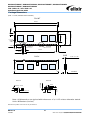
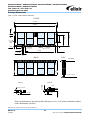
Package Dimensions
[1GB – 2 Ranks, 64Mx16 DDR2 SDRAMs]
67.60
FRONT
SIDE
199
1
39
41
Detail A Detail B
11.40
(2X)
BACK
63.60
Detail A
2.55
0.60
Detail B
0.45
Note: All dimensions are typical with tolerances of +/- 0.15 unless otherwise stated.
Units: Millimeters (Inches)
4.00 +/- 0.10
1.00 +/- 0.1
0.25 MAX
3.80 MAX
1.00 +/- 0.10
2.45
47.40
2.70
4.20
2.15
1.80
4.00
20.00
30.00
6.00
Note: Device position and scale are only for reference.

M2N1G64TUH8D4F / M2N2G64TU8HD4B / M2N1G64TUH8D5F / M2N2G64TU8HD5B
M2N1G64TUH8D6F / M2N2G64TU8HD6B
1GB: 128M x 64 / 2GB: 256M x 64
Unbuffered DDR2 SO-DIMM
REV 1.1 18
07/2008
© NANYA TECHNOLOGY CORPORATION
NANYA reserves the right to change products and specifications without notice.
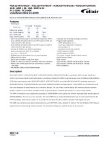
Package Dimensions
[2GB – 2 Ranks, 128M x8 DDR2 SDRAMs]
67.60
FRONT
SIDE
1991 41
Detail A Detail B
4.00
20.00
30.00
6.00
(2X)
BACK
63.60
39
Detail A
2.55
0.60
Detail B
0.45
Note: All dimensions are typical with tolerances of +/- 0.15 unless otherwise stated.
Units: Millimeters (Inches)
4.00 +/- 0.10
1.00 +/- 0.1
0.25 MAX
3.80 MAX
1.00 +/- 0.10
2.45
47.40
2.70
4.20
11.402.15
1.80
Note: Device position and scale are only for reference.

M2N1G64TUH8D4F / M2N2G64TU8HD4B / M2N1G64TUH8D5F / M2N2G64TU8HD5B
M2N1G64TUH8D6F / M2N2G64TU8HD6B
1GB: 128M x 64 / 2GB: 256M x 64
Unbuffered DDR2 SO-DIMM
REV 1.1 19
07/2008
© NANYA TECHNOLOGY CORPORATION
NANYA reserves the right to change products and specifications without notice.
Revision Log
Rev
Date
Modification
1.0
03/2008
Official Release
1.1
07/2008
Revision update
Nanya Technology Corporation
Hwa Ya Technology Park 669
Fu Hsing 3rd Rd., Kueishan,
Taoyuan, 333, Taiwan, R.O.C.
Tel: +886-3-328-1688
Please visit our home page for more information: www.nanya.com
Printed in Taiwan
© 2008
-
 1
1
-
 2
2
-
 3
3
-
 4
4
-
 5
5
-
 6
6
-
 7
7
-
 8
8
-
 9
9
-
 10
10
-
 11
11
-
 12
12
-
 13
13
-
 14
14
-
 15
15
-
 16
16
-
 17
17
-
 18
18
-
 19
19


CnMemory 2GB SO-DIMM, DDR2, PC2-6400 User manual
- Category
- Memory modules
- Type
- User manual
Ask a question and I''ll find the answer in the document
Finding information in a document is now easier with AI
Related papers
Other documents
-
 Elixir M2N2G64TU8HG5B-AC Datasheet
-
 Hynix HMP112S6EFR6C-Y5 Datasheet
-
 Elixir M2Y1GH64TU8HD6B-AC Datasheet
-
Transcend JM800QSU-4GK Datasheet
-
 Elixir M2F1G64TU88G4B-AC Datasheet
-
 Hynix HMT41GU7MFR8C-H9 Datasheet
-
 Hynix HMT451U7AFR8C-PBT0 Datasheet
-
-
-
 Hynix HMT351U7CFR8A-PBT0 Datasheet


