Haier L42B1180 User manual

Category
DVD players
Type
User manual
SERVICE MANUAL
LCD TV
Model No. L42B1180
Chassis
MSD318QT
This service information is designed for experienced repair technicians only and is not designed for use by the general public.
It does not contain warnings or cautions to advise non-technical individuals of potential dangers in attempting to service a product.
Products powered by electricity should be serviced or repaired only by experienced professional technicians. Any attempt to service or repair
the product or products dealt with in this service information by anyone else could result in serious injury or death.
Haier Group
©2009 Qingdao Haier Electronics Co., Ltd.
All rights reserved. Unauthorized copying and distribution is a violation of law.
WARNING
1-1. Table of Contents
1. General Information...........................................................................
1-1. Table of Contents
1-3. Important Notice
1
Chapter 1: General Information
1
3
1-2. General Guidelines
1-4. How to Read this Service Manual
3
6
6SHFL¿FDWLRQV....................................................................................
- 01 -
3. Location of Controls and Components...........................................
3-1. Board Location
3-2. Main Board & AV Board
3-3. Power Board
3-4. LCD Panel
4. Disassemble and Assemble..........................................................
4-1 Remove the Pedestal
7
88
8
8
11
12
14
14
4-2 Remove the Back Cover 14
4-3 Remove the Terminal Bracket
15
4-4 Remove the Power Module 15
4-5 Remove the Main Board 15
4-6 Remove the Speaker 16
4-7 Remove the Remote Control Board 16
5. Installation Instructions..…....………………...........………….........
16
5-1 External Equipment Connections 16
5-2 HDMI Connections 20
6. Operation Instructions....…....………………...........………….........
23
6-1 Front Panel Controls
6-2 Back Panel Controls
6-3 Universal Remote Control
23
23
24
7. Electrical Parts…....………………...........………….........................
25
7-1. Block Diagram
7-2. Circuit Diagram
7-3. Wiring Connection Diagram
25
26
35
8. TV Operation........………….............................................................
36
- 02 -
9. Trouble-shooting…………..............................................................
43
9-1. Simple Check 43
9-2. Main Board Failure Check
9-3. Panel Failure
44
53
1-2. General Guidelines
When servicing, observe the original lead dress. If a short circuit is found, replace all parts
which have been overheated or damaged by the short circuit.
After servicing, see to it that all the protective devices such as insulation barriers, insulation
papers shields are properly installed.
After servicing, make the following leakage current checks to prevent the customer from
being exposed to shock hazards.
1) Leakage Current Cold Check
2) Leakage Current Hot Check
3) Prevention of Electro Static Discharge (ESD) to Electrostatically Sensitive
1-3. Important Notice
1-3-1. Follow the regulations and warnings
Most important thing is to list up the potential hazard or risk for the service personnel to
open the units and disassemble the units. For example, we need to describe properly
how to avoid the possibility to get electrical shock from the live power supply or charged
electrical parts (even the power is off).
This symbol indicates that high voltage is present inside.It is dangerous to
make any king of contact with any inside part of this product.
This symbol indicates that there are important operating and maintenance
instructions in the literture accompanying the appliance.
1-3-2. Be careful to the electrical shock
7RSUHYHQWGDPDJHZKLFKPLJKWUHVXOWLQHOHFWULFVKRFNRU¿UHGRQRWH[SRVHWKLV79VHW
to rain or excessive moisture. This TV must not be exposed to dripping or splashing water,
DQGREMHFWV¿OOHGZLWKOLTXLGVXFKDVYDVHVPXVWQRWEHSODFHGRQWRSRIRUDERYHWKH79
1-3-3. Electro static discharge (ESD)
Some semiconductor (solid state) devices can be damaged easily by static electricity. Such
components commonly are called Electrostatically Sensitive (ES) Devices. The following
techniques should be used to help reduce the incidence of component damage caused by
electros static discharge (ESD).
1-3-4. About lead free solder (PbF)
This product is manufactured using lead-free solder as a part of a movement within the
consumer products industry at large to be environmentally responsible. Lead-free solder
must be used in the servicing and repairing of this product.
8VHWKHJHQHZLQJSDUWVVSHFL¿HGSDUWV
Special parts which have purposes of fire retardant (resistors), high-quality sound
(capacitors), low noise (resistors), etc. are used.
When replacing any of components, be sure to use only manufacture's specified parts
shown in the parts list.
Safety Component
Ɣ&RPSRQHQWVLGHQWL¿HGE\PDUNKDYHVSHFLDOFKDUDFWHULVWLFVLPSRUWDQWIRUVDIHW\
- 03 -
1-3-6 Safety Check after Repairment
- 04 -
&RQ¿UPWKDWWKHVFUHZVSDUWVDQGZLULQJZKLFKZHUHUHPRYHGLQRUGHUWRVHUYLFHDUHSXW
in the original positions, or whether there are the positions which are deteriorated around
the serviced places serviced or not. Check the insulation between the antenna terminal or
external metal and the AC cord plug blades. And be sure the safety of that.
General Servicing Precautions
1. Always unplug the receiver AC power cord from the AC power source before;
a. Removing or reinstalling any component, circuit board module or any other receiver
assembly.
b. Disconnecting or reconnecting any receiver electrical plug or other electrical
connection.
c. Connecting a test substitute in parallel with an electrolytic capacitor in the receiver.
CAUTION: A wrong part substitution or incorrect polarity installation of electrolytic
capacitors may result in an explosion hazard.
2. Test high voltage only by measuring it with an appropriate high voltage meter or other
voltage measuring device (DVM, FETVOM, etc) equipped with a suitable high voltage
probe.
Do not test high voltage by "drawing an arc".
5. Do not defeat any plug/socket B+ voltage interlocks with which receivers covered by this
service manual might be equipped.
8VHZLWKWKLVUHFHLYHURQO\WKHWHVW¿[WXUHVVSHFL¿HGLQWKLVVHUYLFHPDQXDO
CAUTION: 'RQRWFRQQHFWWKHWHVW¿[WXUHJURXQGVWUDSWRDQ\KHDWVLQNLQWKLVUHFeiver.
3. Do not spray chemicals on or near this receiver or any of its assemblies.
4. Unless specified otherwise in this service manual, clean electrical contacts only by
applying the following mixture to the contacts with a pipe cleaner, cotton-tipped stick or
comparable non-abrasive applicator; 10% (by volume) Acetone and 90% (by volume)
isopropyl alcohol (90%-99% strength).
CAUTION:7KLVLVDÀDPPDEOHPL[WXUH
8QOHVVVSHFL¿HGRWKHUZLVHLQWKLVVHUYLFHPDQXDOOXEULFDWLRQRIFRQWDFWVLVQRWUHTXLUHG
Capacitors may result in an explosion hazard.
6. Do not apply AC power to this instrument and/or any of its electrical assemblies unless
all solid-state device heat sinks are correctly installed.
7. Always connect the test receiver ground lead to the receiver chassis ground before
connecting the test receiver positive lead.
Always remove the test receiver ground lead last. Capacitors may result in an explosion
hazard.
9. Remove the antenna terminal on TV and turn on the TV.
10. Insulation resistance between the cord plug terminals and the eternal exposure metal
should be more than Mohm by using the 500V insulation resistance meter.
11. If the insulation resistance is less than M ohm, the inspection repair should be required.
If you have not the 500V insulation resistance meter, use a Tester. External exposure
metal: Antenna terminal Headphone jack
- 05 -
Electrostatically Sensitive (ES) Devices
1-3-7. Ordering Spare Parts
1. Immediately before handling any semiconductor component or semiconductor-
equipped assembly, drain off any electrostatic charge on your body by touching a known
earth ground. Alternatively, obtain and wear a commercially available discharging wrist
strap device, which should be removed to prevent potential shock reasons prior to applying
power to the unit under test.
2. After removing an electrical assembly equipped with ES devices, place the assembly
on a conductive surface such as aluminum foil, to prevent electrostatic charge buildup or
exposure of the assembly.
'RQRWXVHIUHRQSURSHOOHGFKHPLFDOV7KHVHFDQJHQHUDWHHOHFWULFDOFKDUJHVVXI¿FLHQW
to damage ES devices.
7. Immediately before removing the protective material from the leads of a replacement
ES device, touch the protective material to the chassis or circuit assembly into which the
device will be installed.
CAUTION: Be sure no power is applied to the chassis or circuit, and observe all other
safety precautions.
3. Use only a grounded-tip soldering iron to solder or unsolder ES devices.
Some semiconductor (solid-state) devices can be damaged easily by static electricity.
Such components commonly are called Electrostatically Sensitive (ES) Devices.
Examples of typical ES devices are integrated circuits and some field-effect transistors
and semiconductor "chip" components. The following techniques should be used to help
reduce the ncidence of component damage caused by static by static electricity.
4. Use only an anti-static type solder removal device. Some solder removal devices not
FODVVL¿HGDVDQWLVWDWLFFDQJHQHUDWHHOHFWULFDOFKDUJHVVXI¿FLHQWWRGDPDJH(6GHYLFHV
6. Do not remove a replacement ES device from its protective package until immediately
before you are ready to install it.
(Most replacement ES devices are packaged with leads electrically shorted together by
conductive foam, aluminum foil or comparable conductive material).
8. Minimize bodily motions when handling unpackaged replacement ES devices.
(Otherwise harmless motion such as the brushing together of your clothes fabric or the
OLIWLQJRI\RXUIRRWIURPDFDUSHWHGÀRRUFDQJHQHUDWHVWDWLFHOHFWULFLW\VXI¿FLHQWWRGDPDJH
an ES device.)
Please include the following informations when you order parts. (Particularly the Version
letter)
1. Model number, Serial number and Software Version
The model number and Serial number can be found on the back of each product and the
Software Version can be found at the Spare Parts List.
2. Spare Part No. and Description
<RXFDQ¿QGWKHPLQWKH6SDUH3DUWV/LVW
- 06 -
1-3-8. Photo used in this manual
The illustration and photos used in this Manual may not base on the final design of
products, which may differ from your products in some way.
1-4. How to Read this Service Manual
Using Icons:
,FRQVDUHXVHGWRDWWUDFWWKHDWWHQWLRQRIWKHUHDGHUWRVSHFL¿FLQIRUPDWLRQ7KHPHDQLQJRI
each icon is described in the table below:
Note:
A “note” provides information that is not indispensable, but may nevertheless be valuable
to the reader, such as tips and tricks.
Caution:
A “caution” is used when there is danger that the reader, through incorrect manipulation,
may damage equipment, loose data, get an unexpected result or has to restart(part of) a
procedure.
Warning:
A “warning” is used when there is danger of personal injury.
Reference:
A “reference” guides the reader to other places in this binder or in this manual, where he/
VKHZLOO¿QGDGGLWLRQDOLQIRUPDWLRQRQDVSHFL¿FWRSLF
Service Manual
Model No.:
- 07 -
2. Speci¿cations
Model L42B1120
Screen Size 42 inch
Aspect Ratio 16:9
Resolution 1920*1080
Response Time (ms)
6.5 (GRAY TO
GRAY)
Angel of View
+88/-88(H), +88/-88
(V) Typ.
Color Display 16.7M
No. of Preset Channels
Cable :1-135/ Air:
2-69(ATV&DTV)
OSD Language English
Color System NTSC/PAL/SECAM
Audio System M
Audio Output Power
(Built-in) (W)
8W×2
Audio Output Power
(outer) (W)
No
Total Power Input (W)
240W
Voltage Range (V) AC100V-240V
Power Frequency (Hz) 50~60Hz
Net Weight (KG)
Gross Weight (KG)
Net Dimension (MM) 1015*230*712
Packaged Dimension
(MM)
1215*190*750
22.5
25.7
- 08 -
3. Location of Controls and Components
3-1 Board Location
3-2 Main Board
No. Description
A Board Main Board
B Board Power Board
A Board
B Board
- 09 -
3-2-1 Function Description:
Main Board
Process signal which incept from exterior equipment then translate into signal that panel
can display.
3-2-2 Connector defnition
Main board connector
Power connectors (J15ˈJ16)
J16
J15
Pin number Signal name Pin number Signal name
1 +5V 1 GND
GND
3 DIM 3 +5V
4
high voltage
4 +5V
5 GND 5 POWER ON/OFF
6 +5VSTB
7 +5V
8 +5V
9 GND
10 GND
11 GND
12 +12V
13 +12V
Notes:
J16-Pin 2: Backlight on/off:
The system can t urn o n or turn o ff t he backlight of TFT L CD P anel t hrough the power
supply unit path.
CN115-Pin 5: System power on / standby
System board will use this pin to control system power.
J16-Pin 3: Control the luminance of backlight
The system can generate the P WM s ignal to control the strength of TFT LCD Panel’s
backlight through this connector
2
2
BL
J15
- 10 -
Pin number Signal name Description
1 LED_R LAMP RED
2 LED_G LAMP GREEN
3
4 IR REMOTE CONTROL
5 GND GND
6 5V POWER FOR REMOTE
Pin number Signal name Description
1 KEY1
2 KEY0
3 GND
remote connector (J6)
Keypad and connector (J7)
3-3. Power Board
3-3-1 Function Description:
Supply power for Main board, Panel.
&RQQHFWRUGH¿QLWLRQ
- 11 -
Speaker connector J11
Pin number Signal nameD escription
+KPSR+KPSR1
-KPSR-KPSR2
-KPSL-KPSL3
+KPSL+KPSL4
CN3
CN2
Pin number Signal name Pin number Signal name
9 GND
GND
GND
GND
GND
10 GND
11 GND
12 +12V
13 +12V
POWER ON/OFF
+5VSTB
+5V
+5V
3-4. LCD Panel
- 12 -
T420HW06 V2
AU
CN1
- 13 -
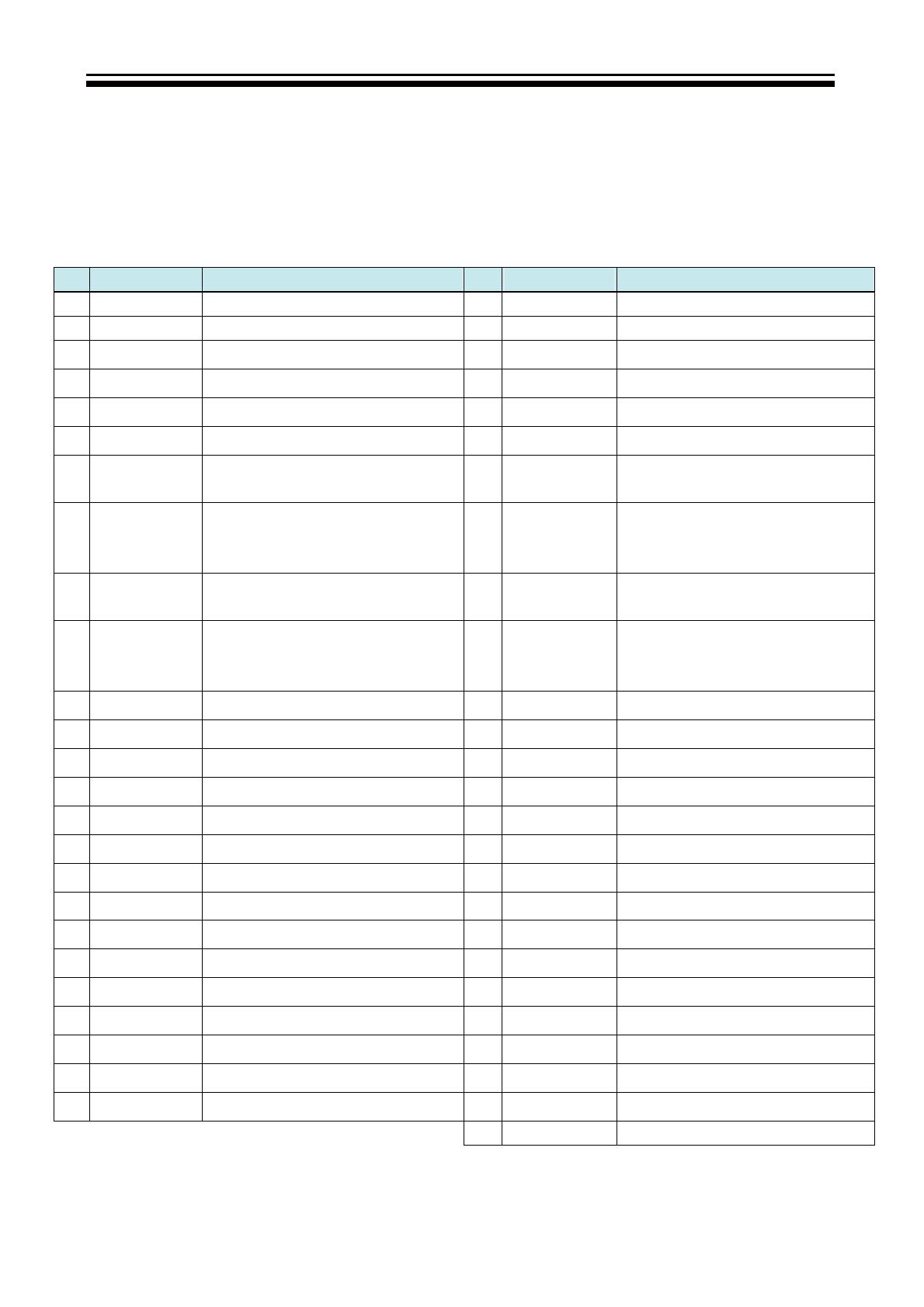
3-4-1 Function Description: Display the signal.
&RQQHFWRUGH¿QLWLRQ
PIN Symbol Description PIN Symbol Description
1 GND Ground 26 GND Ground
2 NC No connection 27 GND Ground
3 Reserved AUO Internal Use Only 28
CH2_0- LVDS Channel 2, Signal 0-
4 Reserved AUO Internal Use Only 29
CH2_0+ LVDS Channel 2, Signal 0+
5 NC No connection 30
CH2_1- LVDS Channel 2, Signal 1-
6 Reserved AUO Internal Use Only 31
CH2_1+ LVDS Channel 2, Signal 1+
7 LVDS_SEL
Open/High(3.3V) for NS,
Low(GND) for JEIDA
32
CH2_2- LVDS Channel 2, Signal 2-
8
Reserved
(VBR_EXT)
PWM Dimming signal input
(AC : 0~3.3V, max:4V,
Duty : 60~100%, freq : 120~240Hz)
33
CH2_2+ LVDS Channel 2, Signal 2+
9
Reserved
(OPC_OUT)
PWM Dimming signal output
(AC:0~3.3V)
34
GND Ground
10
Reserved
(OPC Enable)
Enable DCR function
Enable:3.3V(max:4V),
Disable:0V(or Open)
35
CH2_CLK- LVDS Channel 2, Clock -
11 GND Ground 36
CH2_CLK+ LVDS Channel 2, Clock +
12
CH1_0- LVDS Channel 1, Signal 0-
37
GND Ground
13
CH1_0+ LVDS Channel 1, Signal 0+
38
CH2_3- LVDS Channel 2, Signal 3-
14
CH1_1- LVDS Channel 1, Signal 1-
39
CH2_3+ LVDS Channel 2, Signal 3+
15
CH1_1+ LVDS Channel 1, Signal 1+
40
Reserved AUO Internal Use Only
16
CH1_2- LVDS Channel 1, Signal 2-
41
Reserved AUO Internal Use Only
17
CH1_2+ LVDS Channel 1, Signal 2+
42 GND Ground
18
GND Ground
43 GND Ground
19
CH1_CLK- LVDS Channel 1, Clock -
44 GND Ground
20
CH1_CLK+ LVDS Channel 1, Clock +
45 GND Ground
21
GND Ground
46 GND Ground
22
CH1_3- LVDS Channel 1, Signal 3-
47 NC No connection
23
CH1_3+ LVDS Channel 1, Signal 3+
48 V
DD
Power Supply, +12V DC Regulated
24
Reserved AUO Internal Use Only
49 V
DD
Power Supply, +12V DC Regulated
25
Reserved AUO Internal Use Only
50 V
DD
Power Supply, +12V DC Regulated
51 V
DD
Power Supply, +12V DC Regulated
4. Disassemble and assemble
4-1 Remove the Pedestal 4-3. Remove the adhesive tape
(The location of the adhesive tape as follows)
Remove the adhesive tape indicated on the
¿JXUHDERYH
/D\GRZQWKHXQLWVRWKDWUHDUFRYHU
faces upward
5HPRYHWKHIRXUVFUHZIURPWKH
UHDUFRYHULQGLFDWHGZLWKż
7KHQUHPRYHWKHSHGHVWDO
4-2Remove the Back Cover
5HPRYHWKHWKHVHVFUHZLQGLFDWHGRQ
¿JXUHDERYHE\ż
7KHQUHPRYHWKHEDFNFRYHUIURPWKH
unit.
- 14 -
4-3 Remove the Terminal Bracket
5HPRYHWKHIRXUVFUHZLQGLFDWHGRQ
WKH¿JXUHDERYHE\ż
7KHQSXWWKHWHUPLQDOEUDFNHWWRWKHVLGH
4-4 Remove the power module
5HPRYHWKHIRXUVFUHZLQGLFDWHGRQWKH
¿JXUHDERYHE\ż
7KHQUHPRYHWKHSRZHUPRGXOH
4-5 Remove the Main board
5HPRYHWKHWZRVFUHZLQGLFDWHG
RQWKH¿JXUHDERYHE\ż
'LVFRQQHFWHGWKHFRXSOHU-
J6 J7 J9 J15 J16 J11
5HPRYHWKH0DLQERDUG
- 15 -
CN513
4-6 Remove the speaker
Take out the speaker
4-7 Remove the remote control
Remove the screw, take out the remote
control board
- 16 -
5. Installation Instructions
5-1 External Equipment Connections
Accessories
Remote Control
User GUIDE
Battery
1
ENTER
RETURN
DISPLAY
2
3
4
5 6
7 8 9 0
+
CH
_
+
_
VOL
SUBTITLE AUDIO
SLEEP V-CHIP CC
AUTO
S.M
EXIT
P.M
TV DISPLAY
SOURCE
MENU
MTS/SAP
MUTE
POWER
ASPECT
DVD/USB
RECALL
GOTO MENU SETUP
- 17 -
- 18 -
- 19 -
  • Page 1 1
  • Page 2 2
  • Page 3 3
  • Page 4 4
  • Page 5 5
  • Page 6 6
  • Page 7 7
  • Page 8 8
  • Page 9 9
  • Page 10 10
  • Page 11 11
  • Page 12 12
  • Page 13 13
  • Page 14 14
  • Page 15 15
  • Page 16 16
  • Page 17 17
  • Page 18 18
  • Page 19 19
  • Page 20 20
  • Page 21 21
  • Page 22 22
  • Page 23 23
  • Page 24 24
  • Page 25 25
  • Page 26 26
  • Page 27 27
  • Page 28 28
  • Page 29 29
  • Page 30 30
  • Page 31 31
  • Page 32 32
  • Page 33 33
  • Page 34 34
  • Page 35 35
  • Page 36 36
  • Page 37 37
  • Page 38 38
  • Page 39 39
  • Page 40 40
  • Page 41 41
  • Page 42 42
  • Page 43 43
  • Page 44 44
  • Page 45 45
  • Page 46 46
  • Page 47 47
  • Page 48 48
  • Page 49 49
  • Page 50 50
  • Page 51 51
  • Page 52 52
  • Page 53 53
  • Page 54 54
  • Page 55 55
  • Page 56 56
  • Page 57 57

Haier L42B1180 User manual

Category
DVD players
Type
User manual

Ask a question and I''ll find the answer in the document

Finding information in a document is now easier with AI