Page is loading ...


AS3701B Standard Board
ams Eval Kit Manual
Page 2
[v1-01] 2015-May-21
Document Feedback
Table of Contents
1 Introduction .......................................................................................................................... 3
1.1 Kit Content ........................................................................................................................... 4
2 Getting Started ..................................................................................................................... 5
3 Hardware Description........................................................................................................... 6
4 Software Description .......................................................................................................... 10
4.1 LDO, DCDC ....................................................................................................................... 11
4.2 GPIO .................................................................................................................................. 13
4.3 Housekeeping .................................................................................................................... 15
4.4 OTP .................................................................................................................................... 17
4.5 Charger .............................................................................................................................. 20
5 Schematics, Layers and BOM ........................................................................................... 24
5.1 Schematics of AS3701 Evaluation Board .......................................................................... 25
5.2 Board Layout of AS3701 Evaluation Board ....................................................................... 28
5.3 BOM ................................................................................................................................... 32
6 Ordering & Contact Information ......................................................................................... 33
7 Copyrights & Disclaimer ..................................................................................................... 34
8 Revision Information .......................................................................................................... 35

AS3701B Standard Board
ams Eval Kit Manual
Page 3
[v1-01] 2015-May-21
Document Feedback
1 Introduction
This document describes the AS3701 Evaluation Kit.
The AS3701 is a small compact PMU for small size and low power applications.
AS3701 features one 500mA DCDC buck converter operating from 1MHz up to 4MHz, two
200mA LDOs, two 40mA current sinks and offers additional GPIO functions. Further, the device
contains an integrated linear battery charger with constant current and constant voltage
operation. The wide charging current range going from 11mA up to 500mA and the integrated
battery temperature monitoring with selectable NTC beta values make this device suitable for a
great variety of applications.
The single supply voltage may vary from 2.7V to 5.5V and all functionalities of AS3701 can be
controlled via the I2C interface.
The Evaluation Kit has to be externally supplied. The graphical user interface (GUI) runs on PC
running Windows 7 and allows the user to control the AS3701. Use the enclosed USB cable to
connect the PC with the Evaluation board.

AS3701B Standard Board
ams Eval Kit Manual
Page 4
[v1-01] 2015-May-21
Document Feedback
1.1 Kit Content
The AS3701 Evaluation Kit includes all items listed in Figure 1: Kit Content.
Figure 1: Kit Content
Label
Item
Comment
A
Evaluation Board
AS3701B Micro-PMIC
B
USB flash drive
Includes Eval Kit Manual and Software
C
USB connection cable
-
A
B
C

AS3701B Standard Board
ams Eval Kit Manual
Page 5
[v1-01] 2015-May-21
Document Feedback
2 Getting Started
Drive the AS3701 Eval Kit only with the recommended settings and values as described in the
datasheet. (Please check www.ams.com for the latest version.)
For a detailed description of the Kit please read carefully sections 3-5 of this document.
Check all Jumpers for the default setting (factory-set) shown in Figure 1: Kit Content
Install the GUI (GUI can be found on the included USB flash drive)
Establish the connection between PC and Evaluation board via the enclosed USB cable
(connector “U2”)
Supply the Board via the charger input either through VUSB (USB Mini “U5” ) or VUSB (“BU1”)
and GND or through a Li-Ion battery connected to VBAT (“BU3”) and GND
Start the GUI
If prompted perform a firmware upgrade on the Evaluation board in order to ensure a proper
communication to the GUI! The appropriate firmware file for the Evaluation board comes with
the GUI software and can be found in the GUI installation directory
Never disconnect the supply or interrupt the connection to the PC during the update!
If the AS3701 Evaluation Board is supplied and connected properly to the PC and the
appropriate firmware file is installed, both fields at the right bottom corner of the GUI turn green.

AS3701B Standard Board
ams Eval Kit Manual
Page 6
[v1-01] 2015-May-21
Document Feedback
3 Hardware Description
The AS3701 Evaluation Board can be powered via battery, external power supply, or USB.
With the integrated linear charger Li-Ion batteries can be charged.
Figure 2: Evaluation Board Overview
Label
Name
Designator
Description
Info
A
VBAT,GND
BU3, BU4
VBAT
Li-Ion battery connector
B1
VUSB
U5
USB Mini
Charger adapter input
B2
VUSB, GND
BU1, BU2
VUSB
Charger adapter input
C
VEXT, GND
BU5, BU6
VEXT
External supply for current sinks
B1
C
H
G
E
A
I
J
K
D
F
B2

AS3701B Standard Board
ams Eval Kit Manual
Page 7
[v1-01] 2015-May-21
Document Feedback
Label
Name
Designator
Description
Info
D
NTC
J10, R12
NTC resistor
Connector for external NTC
resistor “J12” + parallel restistor
“R12”
E
AS3701
U1
PMIC
AS3701B Micro-PMIC (20-ball
WL-CSP)
F
J12
J12
I2C connector
-
G
J13
J13
Programming
interface
-
H
U2
U2
USB Mini
Interface between board and PC
I
ON slide
S3
ON slide
ON-key switch
J
ON push
S1
ON push
ON-key push button
K
XRES
S2
XRES
Reset button

AS3701B Standard Board
ams Eval Kit Manual
Page 8
[v1-01] 2015-May-21
Document Feedback
Figure 3: Jumper locations
Label
Name
Designator
Description
Info
A
VCURRx
J3
Supply for sinks
Selection of current sinks supply (via
ext. supply or via VSUP)
B
XIRQ_NTC→PU
J11
XIRQ pull-up
Place jumper to connect pullup R4 to
XIRQ_NTC pin
C
GPIO1
CURR1
J4
GPIO1
CURR1
Place jumper to connect GPIO1 to an
indication LED
CURR1: GPIO1 connected to D2
(current sink mode)
GPIO1: GPIO1 connected to D4
via R7 (GPIO mode)
C
A
E
J
I
B
D
F
H
G
L
K

AS3701B Standard Board
ams Eval Kit Manual
Page 9
[v1-01] 2015-May-21
Document Feedback
Label
Name
Designator
Description
Info
D
XIRQ_NTC→NTC,
GPIO3→NTC,
GPIO4→NTC,
J1, J7, J15
Input pin for
NTC resistor
Place jumper to connect NTC resistor
(J10, R12) to
XIRQ_NTC (J1)
J11 must be removed!
GPIO3 (J7)
GPIO4 (J15)
E
GPIO2
CURR2
J5
GPIO2
CURR2
Place jumper to connect GPIO2 to an
indication LED
CURR2: GPIO2 connected to D3
(current sink mode)
GPIO2: GPIO2 connected to D5
via R8 (GPIO mode)
F
SCL→PU
SDA→PU
J14, J16
I2C Pull-up
resistors to
VSUP
Place Jumpers to connect I2C Pull-up
resistors to VSUP
SCL→PU (J14)
SDA→PU (J16)
G
GPIO3, GPIO4,
GPIO5
J2, J6, J8
GPIO3, GPIO4,
GPIO5
Place jumper to connect GPIOx to LED
for indication
H
SCL, SDA
J19, J20
I2C connection
between µC and
AS3701
Place Jumper to connect I2C Interface
of onboard uC to AS3701
I
J25
J25
ON push to
VSUP/GND
Place jumper to connect S1 either to
VSUP or to GND
non-inverted: ON push→VSUP
inverted: ON push→GND
J
J29
J29
ON-key
push/slide
Configure ON-key as push button or as
switch (slider)
slider push button
K
J26
J26
ON push to
pull- up/down
Place jumper to connect ON pin either
to pull-up (R19) or to pulldown (R2)
non-inverted: ON push→pull-down
inverted: ON push→pull-up
L
LED
J27
Status LED
Place jumper to enable the status LED

AS3701B Standard Board
ams Eval Kit Manual
Page 10
[v1-01] 2015-May-21
Document Feedback
4 Software Description
The graphical user interface (GUI) is used to control the AS3701 Evaluation board.
Start the GUI and make sure that the Hardware settings are according to chapter 2, Getting
Started.
Check if hardware is recognized and indicators in the bottom right corner of the GUI are green
colored.
Figure 4: AS3701 Evaluation Software

AS3701B Standard Board
ams Eval Kit Manual
Page 11
[v1-01] 2015-May-21
Document Feedback
4.1 LDO, DCDC
The AS3701 features 2 LDO’s and 1 DCDC Step-down converter
Figure 5: Regulator tab
Label
Name
Comment
A
SD on
Enabling / Disabling of DCDC
B
Vout Regulator
Output voltage setting
C
Frequency/
Select switching frequency
D
DVM Control
With DVM the output voltage will ramp up/down with a selectable
slope after the new value was written to the registers
E
GPIO Control
GPIO controlling of DCDC
F
LDO on
Enabling / Disabling of LDO
G
Vout Regulator
Output voltage setting
H
Current Limit
Current Limit setting
A
B
C
D
E
F
G
H
I


AS3701B Standard Board
ams Eval Kit Manual
Page 13
[v1-01] 2015-May-21
Document Feedback
4.2 GPIO
The AS3701A features 2 GPIOs and AS3701B features 5 GPIOs
Figure 6: GPIO tab
Label
Name
Comment
A
GPIO1,2,3,4,5
“GPIO x HIGH”: Determines the output signal on GPIOx pin
when selected as output source
“GPIO x HIGH”: Indicates the logic level on GPIOx pin when
configured as digital input pin
“GPIO x invert”: Setting of GPIOx to normal or inverted
“GPIO x mode”: Selects the GPIOx mode
“GPIO x IO”: Selects the GPIOx special function
B
CURR1,2
(GPIO1,2)
“CURRx Low Voltage”: Bit is set when voltage of current sink
drops below low voltage threshold (1ms debounce time default)
CURRx slider: Defines the current into CURRx
A
B
C

AS3701B Standard Board
ams Eval Kit Manual
Page 14
[v1-01] 2015-May-21
Document Feedback
Label
Name
Comment
C
Stand-by /
Voltage Control
per GPIO
Assign any GPIOx for both “Regulator Control x” slots
GPIO1 and GPIO2 may be used to control two regulator
separately
“Vselect+Stand-by”: Additionally to the Vselect function the
defined GPIOx (GPIO Control) can be used to enter Stand-by
mode
For further details please refer to the AS3701 datasheet

AS3701B Standard Board
ams Eval Kit Manual
Page 15
[v1-01] 2015-May-21
Document Feedback
4.3 Housekeeping
In this section the Reset/Power Off behavior, ON-key configuration, PWM setting, Temperature
Supervision, Stand-by options and Interrupts can be defined.
Figure 7: Housekeeping tab
Label
Name
Comment
A
Reset / Power
Off
“Reset Voltage Fall”: Selection of the reset level for falling VSUP
“Reset Timer”: Set Reset Time, after the last regulator has
started
“Power off at VSUP low”: Enter power off mode if low VSUP is
detected (Pin ON=low and bit auto_off=0)
0: If low VSUP is detected, VSUP is continuously monitored and
chip startup initiated if VSUP is above ResVoltRise
1: If low VSUP is detected, enter power off mode
Note: low VSUP level depends on setting for “Supply Reset enable”
“Supply Reset enable”
0: A reset is generated if VSUP < 2.7V
1: A reset is generated if VSUP < ResVoltFall
A
B
C
D
E

AS3701B Standard Board
ams Eval Kit Manual
Page 16
[v1-01] 2015-May-21
Document Feedback
Label
Name
Comment
“Fast reset enable”
0: Vresetfall debounce time = 3msec
1: Vresetfall debounce time = 64usec
“auto off”: Indicator for “auto off” bit (setting in OTP)
B
ON key
Indicator for ON key mode, push-button or switch (setting in
OTP)
Indicator of ON key status
“longpress” function
Select the ON key longpress behavior (power off, reset)
Select the ON key longpress delay time (4s, 8s)
C
PWM
“PWM high time”: Defines the high time of the PMW generator
“PWM low time”: Defines the low time of the PMW generator
“PMW divider”: Defines the divider ratio of the prescaler for the
PWM generator
Note: For GPIO1 and GPIO2, the PWM output signal can be
visualized via the Current sinks
D
Temperature
Supervision
Switch ON/OFF temperature supervision (default ON)
All other bits (in reg. 37h) are only valid if temperature
supervision is 1! Leave at 1, do not disable
Indicator that 110°C threshold has been reached
Indicator that 140°C threshold has been reached
By reaching 140°C a reset cycle is started - this flag is not reset
by an over temperature caused reset and has to be reset by
“Reset Overtemp 140” button (optionally reset by writing 1 and
afterwards 0 to rst_ov_temp_140 in addr:37h)
E
Stand-by Options
off-delay: Set Delay between I²C command, GPIO or Reset
signal for power_off, standby mode or reset and execution of
that command
“Stand-By Reset Disable”
0: Normal mode, reset is active in standby mode
1: No reset in standby mode and during exit of standby mode
“Stand-by” button: Enter Stand-by mode
“Stand-by Regulator”: Define which regulators should be enabled
during Stand-by mode

AS3701B Standard Board
ams Eval Kit Manual
Page 17
[v1-01] 2015-May-21
Document Feedback
4.4 OTP
This section defines the startup sequence and enables programing of OTP.
Figure 8: OTP tab - Startup
Label
Name
Comment
A
Timeslots
4 Timeslots (Startup sequentially beginning with Timeslot 1), to
every single timeslot a delay can be added
For each timeslot one of the available regulators or available GPIOs
can be defined
LDO settings: voltage and current limit
DCDC settings: voltage and frequency (“sd1_frequ”)
Select between low (1/2 MHz) and high (3/4 MHz) frequency
0: 1 MHz if sd1_fsel=0, 2MHz if sd1_fsel=1
1: 3 MHz if sd1_fsel=0, 4MHz if sd1_fsel=1
GPIO settings: normal or inverted, GPIO mode and GPIO IO special
function (GPIOx_iosf)
B
General Settings
“Delay Interval”: Selection of 1ms or 4ms delay which can be
enabled for each timeslot
“Reset Time”: Set Reset Time, after the last regulator has started
A
B
C

AS3701B Standard Board
ams Eval Kit Manual
Page 18
[v1-01] 2015-May-21
Document Feedback
Label
Name
Comment
“Reset Voltage Rise”: Selection of the reset level for rising VSUP
It’s recommended to set the ResVoltRise level 200mV above
ResVoltFall level to have a hysteresis
“SD1 frequ selection”: Select between low and high frequency
range
0: 1 MHz if sd1_frequ=0, 3MHz if sd1_frequ=1
1: 2 MHz if sd1_frequ=0, 4MHz if sd1_frequ=1
“ON key switch”: Selects the mode of ON input
0: ON key works as push-button
1: ON key works as switch (slider)
The setting for ON key mode in the software must comply with
the setting on the hardware!
For the correct jumper setting of the ON key input please see
section J in Figure 3: Jumper locations
“ON key invert”: inverts the ON input
0: ON input is active high (default)
1: ON input is active low
The setting for ON key invert in the software must comply with
the setting on the hardware!
For the correct jumper setting of the ON key input please see
section I,K in Figure 3: Jumper locations
In case ON key is configured as slider (hardware/software) no
further settings are necessary
“auto off”: Defines startup behavior at first battery insertion
0: Startup of chip if VBAT>ResVoltRise
1: Enter power OFF mode (Startup with ON key or charger
insertion)
C
OTP
Loading of existing OTP startup sequence
Saving OTP startup sequence as a .txt file
Reading the OTP registers of the chip
Writing into the OTP registers of the chip
Testing the startup from the OTP registers


AS3701B Standard Board
ams Eval Kit Manual
Page 20
[v1-01] 2015-May-21
Document Feedback
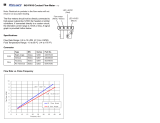
4.5 Charger
In this section the Charger settings can be defined.
Figure 10: Charger tab - General
Label
Name
Comment
A
Charger /
Preregulator
Configuration
“USB Current”: USB input current limit
“VSUP Voltage”: Voltage regulation of VSUP of the input current
limiter
“USB limiter enable”: ON/OFF control of USB charger input
“Charging enable”: Enables charging, “USB limiter enable” must
be set to ON
“Charger Detection disable”: turn OFF charger detection circuit
for power OFF state
0: Charger detection is always enabled
1: Charger detection is disabled in power-OFF state
A
B
C
D
E
/