
Date: May, 2006 / Issue 1.0
Service Manual Model : KG320
Service Manual
KG320

- 3 -
1. INTRODUCTION...................................5
1.1 Purpose ..................................................... 5
1.2 Regulatory Information ............................... 5
1.3 Abbreviations .............................................. 7
2. PERFORMANCE ..................................9
2.1 H/W Features...............................................9
2.2 Technical Specification ..............................10
3. TECHNICAL BRIEF............................15
3.1 Transceiver (SI4210, U401).......................15
3.2 Power Amplifier (SKY77328, U400) ......... 20
3.3 26 MHz Clock (VCTCXO, X400)................22
3.4 FEM for Triband(FL400) ............................22
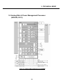
3.5 Digital Main Processor
(AD6527B, U102) ......................................24
3.5 Analog Main & Power Management
Processor (AD6535, U101)........................29
3.6 Charging IC (ISL6299, U205) ....................37
3.7 CAMERA IC(AIT811T,U103) .....................40
3.8 MIDI IC(YMU787,U202).............................42
3.9 Keypad Switches and Scanning ................46
3.10 Microphone ..............................................47
3.11 Main Speaker...........................................47
3.12 Headset Interface ....................................48
3.13 MEMORY(TOSHIBA, U204)....................49
3.14 BLUETOOTH(LBMA-2C67B2,U202).......50
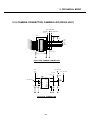
3.15 CAMERA CONNECTOR, CAMERA
LDO(CN202,U201) ..................................51
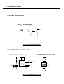
3.16 KEY BACKLIGHT ....................................52
3.17 WHITE/FLASH LED LDO ........................52
3.18 FLIP SWITCH (U105) ..............................53
3.19 VIBRATOR ..............................................53
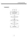
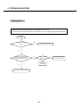
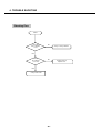
4. TROUBLE SHOOTING.......................54
4.1 RX Trouble.................................................54
4.2 TX Trouble .................................................60
4.3 Power On Trouble......................................67
4.4 Charging Trouble .......................................69
4.5 Vibrator Trouble .........................................71
4.6 LCD Trouble ..............................................73
4.7 BT Trouble .................................................76
4.8 Speaker Trouble ........................................79
4.9 SIM Card Interface Trouble .......................81
4.10 Earphone Trouble ....................................83
4.11 Receiver Trouble .....................................85
4.12 Microphone Trouble.................................87
4.13 RTC Trouble ............................................89
4.14 Camera and Flash Trouble ......................91
5. DOWNLOAD AND CALIBRATION.....94
5.1 Download...................................................94
6. BLOCK DIAGRAM .............................99
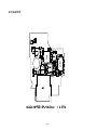
7. Circuit Diagram................................101
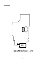
8. pcb layout ........................................108
9. ENGINEERING MODE......................115
9.1 BB Test [MENU 1] ...................................116
9.2 RF Test [MENU 2] ...................................118
9.3 MF mode [MENU 3] .................................118
9.4 Trace option [MENU 4] ............................119
9.5 Call timer [MENU 5] .................................119
9.6 Fact. Reset [MENU 6]..............................119
9.7 S/W version .............................................119
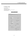
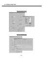
10. STAND ALONE TEST ....................130
10.1 Introduction ............................................120
10.2 Setting Method.......................................120
10.3 Means of Test ........................................121
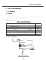
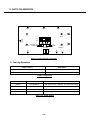
11. AUTO CALIBRATION .....................123
11.1 Calibration..............................................123
11.2 AGC .......................................................127
11.3 APC .......................................................127
11.4 ADC .......................................................127
11.5 Setting....................................................127
11.6 How to do calibration .............................127
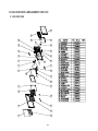
12. EXPLODED VIEW & REPLACEMENT
PART LIST ..................................... 129
12.1 Exploded View ...................................... 129
12.2 Replacement Parts ................................131
12.3 Accessory ............................................. 147
Table Of Contents

- 4 -

1. INTRODUCTION
- 5 -
1.1 Purpose
This manual provides the information necessary to repair, calibration, description and download the
features of this model.
1.2 Regulatory Information
A. Security
Toll fraud, the unauthorized use of telecommunications system by an unauthorized part (for example,
persons other than your company’s employees, agents, subcontractors, or person working on your
company’s behalf) can result in substantial additional charges for your telecommunications services.
System users are responsible for the security of own system. There are may be risks of toll fraud
associated with your telecommunications system. System users are responsible for programming and
configuring the equipment to prevent unauthorized use. The manufacturer does not warrant that this
product is immune from the above case but will prevent unauthorized use of common-carrier
telecommunication service of facilities accessed through or connected to it.
The manufacturer will not be responsible for any charges that result from such unauthorized use.
B. Incidence of Harm
If a telephone company determines that the equipment provided to customer is faulty and possibly
causing harm or interruption in service to the telephone network, it should disconnect telephone
service until repair can be done. A telephone company may temporarily disconnect service as long as
repair is not done.
C. Changes in Service
A local telephone company may make changes in its communications facilities or procedure. If these
changes could reasonably be expected to affect the use of the this phone or compatibility with the
network, the telephone company is required to give advanced written notice to the user, allowing the
user to take appropriate steps to maintain telephone service.
D. Maintenance Limitations
Maintenance limitations on this model must be performed only by the manufacturer or its authorized
agent. The user may not make any changes and/or repairs expect as specifically noted in this manual.
Therefore, note that unauthorized alternations or repair may affect the regulatory status of the system
and may void any remaining warranty.
1. INTRODUCTION

1. INTRODUCTION
- 6 -
E. Notice of Radiated Emissions
This model complies with rules regarding radiation and radio frequency emission as defined by local
regulatory agencies. In accordance with these agencies, you may be required to provide information
such as the following to the end user.
F. Pictures
The pictures in this manual are for illustrative purposes only; your actual hardware may look slightly
different.
G. Interference and Attenuation
Phone may interfere with sensitive laboratory equipment, medical equipment, etc.Interference from
unsuppressed engines or electric motors may cause problems.
H. Electrostatic Sensitive Devices
ATTENTION
Boards, which contain Electrostatic Sensitive Device (ESD), are indicated by the sign.
Following information is ESD handling:
• Service personnel should ground themselves by using a wrist strap when exchange system boards.
• When repairs are made to a system board, they should spread the floor with anti-static mat which is
also grounded.
• Use a suitable, grounded soldering iron.
• Keep sensitive parts in these protective packages until these are used.
• When returning system boards or parts like EEPROM to the factory, use the protective package as
described.

1. INTRODUCTION
- 7 -
1.3 Abbreviations
For the purposes of this manual, following abbreviations apply:
APC Automatic Power Control
BB Baseband
BER Bit Error Ratio
CC-CV Constant Current - Constant Voltage
DAC Digital to Analog Converter
DCS Digital Communication System
dBm dB relative to 1 milli watt
DSP Digital Signal Processing
EEPROM Electrical Erasable Programmable Read-Only Memory
ESD Electrostatic Discharge
FPCB Flexible Printed Circuit Board
GMSK Gaussian Minimum Shift Keying
GPIB General Purpose Interface Bus
GSM Global System for Mobile Communications
IPUI International Portable User Identity
IF Intermediate Frequency
LCD Liquid Crystal Display
LDO Low Drop Output
LED Light Emitting Diode
OPLL Offset Phase Locked Loop

1. INTRODUCTION
- 8 -
PAM Power Amplifier Module
PCB Printed Circuit Board
PGA Programmable Gain Amplifier
PLL Phase Locked Loop
PSTN Public Switched Telephone Network
RF Radio Frequency
RLR Receiving Loudness Rating
RMS Root Mean Square
RTC Real Time Clock
SAW Surface Acoustic Wave
SIM Subscriber Identity Module
SLR Sending Loudness Rating
SRAM Static Random Access Memory
PSRAM Pseudo SRAM
STMR Side Tone Masking Rating
TA Travel Adapter
TDD Time Division Duplex
TDMA Time Division Multiple Access
UART Universal Asynchronous Receiver/Transmitter
VCO Voltage Controlled Oscillator
VCTCXO Voltage Control Temperature Compensated Crystal Oscillator
WAP Wireless Application Protocol

2. PERFORMANCE
- 9 -
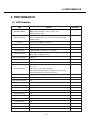
2.1 H/W Features
2. PERFORMANCE
Item Feature Comment
Li-Poly, 600mAh
Standard Battery Battery Size : 36 (W) ×24(H) ×6.5(T) [mm]
Battery Weight : TBD
Under the minimum current consumption environment
Stand by Current (such as paging period 9), the level of standby current
is below 4mA.
Talk time Up to 2 hours (GSM TX Level 5)
Stand by time Up to 200 hours (Paging Period: 9, RSSI: -85 dBm)
Charging time Approx. Under 3.00 hours
RX Sensitivity GSM, EGSM: -104dBm, DCS: -104dBm
TX output power GSM, EGSM : 33dBm(Level 5),
DCS, PCS : 30dBm(Level 0)
GPRS compatibility Class 10
SIM card type 3V Small Only
Display LCD : TFT 176 × 220 pixel 260K Color
Hard icons. Key Pad
0 ~ 9, #, *,
Status Indicator Menu Key, Confirm Key, Shot Key
Send Key, END/PWR Key, Left, Right, Up, Down Key
Soft Key(Left/Right), Hot Key(Left/Right)
ANT Internal
EAR Phone Jack Yes (stereo)
PC Synchronization Yes
Speech coding EFR/FR/HR
Data and Fax Yes
Vibrator Yes
Loud Speaker Yes
Voice Recoding Yes
Microphone Yes
Speaker/Receiver Speaker/Receiver
Travel Adapter Yes
MIDI 64 Poly (Stereo SPK)
MP3/AAC Yes
Options Data Cable

2. PERFORMANCE
- 10 -
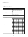
2.2 Technical Specification
Item Description Specification
EGSM
TX: 890 + (n-1024) x 0.2 MHz
RX: 935 + (n-1024) x 0.2 MHz (n=975~1024)
DCS
1Frequency Band TX: 1710 + (n-512) x 0.2 MHz
RX: 1805 + (n-512) x 0.2 MHz (n=512~885)
PCS
TX: 1810 + (n-512) x 0.2 MHz
RX: 1905 + (n-512) x 0.2 MHz (n=512~885)
2Phase Error RMS < 5 degrees
Peak < 20 degrees
3Frequency Error < 0.1 ppm
GSM, EGSM
Level Power Toler. Level Power Toler.
533 dBm 2dB 13 17 dBm 3dB
631 dBm 3dB 14 15 dBm 3dB
729 dBm 3dB 15 13 dBm 3dB
827 dBm 3dB 16 11 dBm 5dB
925 dBm 3dB 17 9 dBm 5dB
10 23 dBm 3dB 18 7 dBm 5dB
11 21 dBm 3dB 19 5 dBm 5dB
4Power Level 12 19 dBm 3dB
DCS, PCS
Level Power Toler. Level Power Toler.
030 dBm 2dB 8 14 dBm 3dB
128 dBm 3dB 9 12 dBm 4dB
226 dBm 3dB 10 10 dBm 4dB
324 dBm 3dB 11 8 dBm 4dB
422 dBm 3dB 12 6 dBm 4dB
520 dBm 3dB 13 4 dBm 4dB
618 dBm 3dB 14 2 dBm 5dB
716 dBm 3dB 15 0 dBm 5dB

2. PERFORMANCE
- 11 -
Item Description Specification
GSM, EGSM
Offset from Carrier (kHz). Max. dBc
100 +0.5
200 -30
250 -33
400 -60
600~ <1,200 -60
1,200~ <1,800 -60
1,800~ <3,000 -63
3,000~ <6,000 -65
5Output RF Spectrum 6,000 -71
(due to modulation) DCS, PCS
Offset from Carrier (kHz). Max. dBc
100 +0.5
200 -30
250 -33
400 -60
600~ <1,200 -60
1,200~ <1,800 -60
1,800~ <3,000 -65
3,000~ <6,000 -65
6,000 -73
GSM, EGSM
Offset from Carrier (kHz) Max. (dBm)
Output RF Spectrum 400 -19
6(due to switching transient) 600 -21
1,200 -21
1,800 -24

2. PERFORMANCE
- 12 -
Item Description Specification
DCS, PCS
Offset from Carrier (kHz). Max. (dBm)
Output RF Spectrum 400 -22
6(due to switching transient) 600 -24
1,200 -24
1,800 -27
7Spurious Emissions Conduction, Emission Status
GSM, EGSM
8Bit Error Ratio BER (Class II) < 2.439% @-102 dBm
DCS, PCS
BER (Class II) < 2.439% @-100 dBm
9RX Level Report Accuracy 3 dB
10 SLR 8 3 dB
Frequency (Hz) Max.(dB) Min.(dB)
100 -12 -
200 0 -
300 0 -12
11 Sending Response 1,000 0 -6
2,000 4 -6
3,000 4 -6
3,400 4 -9
4,000 0 -
12 RLR 2 3 dB
Frequency (Hz) Max.(dB) Min.(dB)
100 -12 -
200 0 -
300 2 -7
500 *-5
13 Receiving Response 1,000 0 -5
3,000 2 -5
3,400 2 -10
4,000 2
*Mean that Adopt a straight line in between 300 Hz and
1,000 Hz to be Max. level in the range.

2. PERFORMANCE
- 13 -
Item Description Specification
14 STMR 13 5 dB
15 Stability Margin > 6 dB
dB to ARL (dB) Level Ratio (dB)
-35 17.5
-30 22.5
-20 30.7
16 Distortion -10 33.3
033.7
731.7
10 25.5
17 Side Tone Distortion Three stage distortion < 10%
18 System frequency 2.5ppm
(13 MHz) tolerance
19 32.768KHz tolerance 30ppm
At least 65 dBspl under below conditions:
20 Ringer Volume 1. Ringer set as ringer.
2. Test distance set as 50 cm
21 Charge Current Fast Charge : < 440 mA
Slow Charge : < 66 mA
Antenna Bar Number Power
5-85 dBm ~
4-90 dBm ~ -86 dBm
22 Antenna Display 3 -95 dBm ~ -91 dBm
2-100 dBm ~ -96 dBm
1-105 dBm ~ -101 dBm
0~ -105 dBm
Battery Bar Number Voltage
03.36 ~ 3.54 V
23 Battery Indicator 1 3.55 ~ 3.66 V
23.67 ~ 3.72 V
33.73 ~ 3.84 V
43.85 V ~
24 Low Voltage Warning 3.55 0.03V (Call)
3.48 0.03V (Standby)

2. PERFORMANCE
- 14 -
Item Description Specification
25 Forced shut down Voltage 3.35 0.03 V
1 Li-Poly Battery
26 Battery Type Standard Voltage = 3.7 V
Battery full charge voltage = 4.2 V
Capacity: 800mAh
Switching-mode charger
27 Travel Charger Input: 100 ~ 240 V, 50/60 Hz
Output: 5.2 V, 800 mA

3. TECHNICAL BRIEF
- 15 -
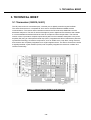
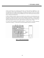
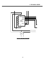
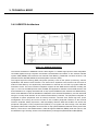
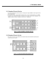
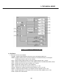
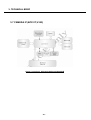
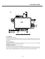
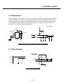
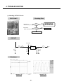
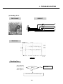
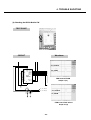
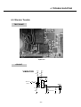
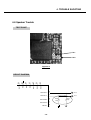
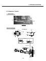
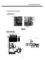
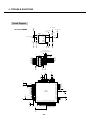
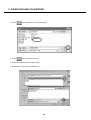
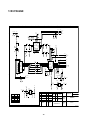
3.1 Transceiver (SI4210, U401)
The RF parts consist of a transmitter part, a receiver part, a digitally-controlled crystal oscillator.
The Aero® II transceiver is a complete RF front end for multi-band GSM and GPRS wireless
communications. The receive section interfaces between the RF band-select SAW filters and the
baseband subsystem. The Aero II receiver leverages a proven digital low-IF architecture and enables
a universal baseband interface without the need for complex dc offset compensation. The transmit
section of Aero II provides a complete upconversion path from the baseband subsystem to the power
amplifier (PA) using an offset phase-locked loop (OPLL) integrated with Silicon Laboratories’ patented
synthesizer technology. All sensitive components, such as TX/RF VCOs, loop filters, tuning inductors,
and varactors are completely integrated into a single integrated circuit. The Aero II transceiver includes
a digitallycontrolled crystal oscillator (DCXO) and completely integrates the reference oscillator and
varactor functionality.
3. TECHNICAL BRIEF
Figure. 3-1 SI4210 TRANSCEIVER BLOCK DIAGRAM

3. TECHNICAL BRIEF
- 16 -
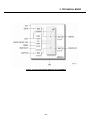
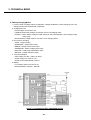
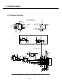
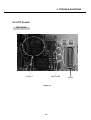
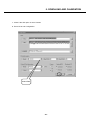
(1) Receiver Part
The Aero II transceiver uses a digital low-IF receiver architecture that allows for the on-chip integration of
the channel selection filters, eliminating the external RF image reject filters, and the IF SAW filter required in
conventional superheterodyne architectures. Compared with direct-conversion architectures, the digital low-
IF architecture has a much greater degree of immunity to dc offsets that can arise from RF local oscillator
(RFLO) self-mixing, second-order distortion of blockers (AM suppression), and device 1/f noise.
The digital low-IF receiver's immunity to dc offsets has the benefit of expanding part selection and improving
manufacturing. At the front end, the common-mode balance requirements on the input SAW filters are
relaxed, and the PCB board design is simplified. At the radio's opposite end, the BBIC is one of the
handset's largest BOM contributors. It is not uncommon for a direct conversion solution to be compatible
only with a BBIC from the same supplier in order to address the complex dc offset issues. However, since
the Aero II transceiver has no requirement for BBIC support of complex dc offset compensation, it is able to
interface to all of the industry leading baseband ICs.
The receive (RX) section integrates four differential input low noise amplifiers (LNAs) supporting the GSM
850 (869-894 MHz), E-GSM 900 (925-960 MHz), DCS 1800 (1805-1880 MHz), and PCS 1900 (1930-1990
MHz) bands. The LNA inputs are matched to 150 or 200 balanced-output SAW filters through external LC
matching networks. See “AN150: Aero II Transceiver PCB Design Guide” for implementation details. The
active LNA input is automatically selected by the ARFCN[9:0] bits and the BANDIND bit in Register 21h. If
performing LNA swapping, the LNASWAP bit in Register 05h is also needed. Please refer to section 4.1.1
for details. The LNA gain is controlled with the LNAG bit in Register 20h.
A quadrature image-reject mixer downconverts the RF signal to a low intermediate frequency (IF). The
mixer output is amplified with an analog programmable gain amplifier (PGA) that is controlled with the
AGAIN[2:0] bits in Register 20h. The quadrature IF signal is digitized with high resolution analog-
todigital converters (ADCs).
Figure. 3-2 SI4210 RECEIVER PART

3. TECHNICAL BRIEF
- 17 -
The ADC output is downconverted to baseband with a digital quadrature local oscillator signal. Digital
decimation and FIR filters perform digital filtering, and remove ADC quantization noise, blockers, and
reference interferers. The response of the FIR filter is programmable to a flat pass band setting (FILTSEL =
0, Register 08h) and a linear phase setting (FILTSEL = 1, Register 08h). After filtering, the digital output is
scaled with a PGA, which is controlled with the DGAIN[5:0] bits in Register 20h.
The LNAG, AGAIN[2:0], and DGAIN[5:0] register bits should be set to provide a constant amplitude signal to
the baseband receive inputs. See “AN153: Aero II Transceiver AGC Strategy” for more details. Digitalto-
analog converters (DACs) drive differential I and Q analog signals onto the BIP, BIN, BQP, and BQN pins to
interface to standard analog-input baseband ICs.
The receive DACs are updated at 1.083 MHz and have a first-order reconstruction filter with a 1 MHz
bandwidth. No special processing is required in the baseband for dc offset compensation. The receive and
transmit baseband I/Q pins are multiplexed together in a 4-wire interface (BIP, BIN, BQP, and BQN). The
common mode level at the receive I and Q outputs is programmable with the DACCM[1:0] bits, and the full
scale level is programmable with the DACFS[1:0] bits in Register 05h.
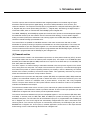
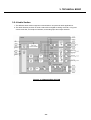
(2) Transmit section
The transmit section consists of an I/Q baseband upconverter, an offset phase-locked loop (OPLL), and two
50 Ω output buffers that can drive an external power amplifier (PA). One output is for the GSM 850 (824-
849 MHz) and E-GSM 900 (880-915 MHz) bands and one output is for the DCS 1800 (1710-1785 MHz) and
PCS 1900 (1850-1910 MHz) bands.
The OPLL requires no external filtering to attenuate transmitter noise and spurious signals in the receive
band, saving both cost and power. The output of the transmit VCO (TXVCO) is a constant-envelope signal
that reduces the problem of spectral spreading caused by non-linearity in the PA. Additionally, the TXVCO
benefits from isolation provided by the transmit output buffers. This significantly minimizes any load pull
effects and eliminates the need for off-chip isolation networks.
A quadrature mixer upconverts the differential in-phase (BIP, BIN) and quadrature (BQP, BQN) baseband
signals to an intermediate frequency (IF) that is filtered and which is used as the reference input to the
OPLL. The OPLL consists of a feedback mixer, a phase detector, a loop filter, and a fully integrated
TXVCO. Low-pass filters before the OPLL phase detector reduce the harmonic content of the quadrature
modulator and feedback mixer outputs.
The transmit I/Q interface must have a non-zero input no later than 94 quarter bits after PDN is asserted for
proper operation. If the baseband is unable to provide a sufficient TX I/Q non-zero input preamble, then the
CWDUR bits in Register 05h can be used to provide a preamble extension.
The receive and transmit baseband I/Q pins are multiplexed together in a 4-wire interface (BIP, BIN, BQP,
and BQN). In transmit mode, the BIP, BIN, BQP, and BQN pins provide the analog I/Q input from the
baseband subsystem. The full-scale level at the baseband input pins is programmable with the BBG[1:0]
bits in Register 05h. The I and Q signals are automatically swapped within the Aero II transceiver when
switching bands. The transmit output path is automatically selected by the ARFCN[9:0] bits and the
BANDIND bits in Register 21h. As an option for multislot applications, direct control of the output transmit
buffers during a burst is offered through the PDTXO bit in Register 23h.

3. TECHNICAL BRIEF
- 18 -
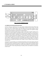
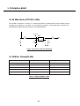
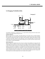
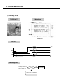
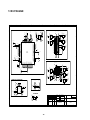
(3) Digitally-controlled crystal oscillator
The Aero II transceiver integrates the DCXO circuitry required to generate a precise system reference clock
using only an external crystal resonator. The DCXO replaces a discrete VC-TCXO module. The DCXO
allows for the use of a standard 26 MHz crystal, which reduces both cost and area compared to using a
VCTCXO module. There are no external varactors or trim capacitors required. This simplifies the design,
programming, and manufacturing compared to less integrated solutions.
The DCXO uses the CDAC and CAFC arrays to correct for both static and dynamic frequency errors,
respectively. An internally digitally programmable capacitor array (CDAC) provides a coarse method of
adjusting the reference frequency in discrete steps. The CDAC[6:0] bits in Register 03h are programmed to
compensate for static variations in PCB design, manufacturing, and crystal tolerance, and are typically set
to center the oscillator frequency during production. A second capacitor array (CAFC) allows for fine and
continuous dynamic adjustment of the reference frequency by an external control voltage (AFC). This
control voltage is supplied by the AFC DAC of the baseband and should be connected to the transceiver
AFC pin (pin 27). The baseband determines the appropriate frequency adjustment based on the receipt of
the FCCH burst. The baseband then adjusts the AFC voltage to correct for frequency variations caused by
temperature drift.
The transceiver can be adjusted for the corresponding baseband AFC input full-scale voltage by setting the
AFCREF bit in Register 04h. Additionally, the Aero II transceiver supports an optional Digital AFC mode for
DCXO operation that is selected by the AFCC bit in Register 04h. In digital mode, the connection between
the baseband and transceiver is eliminated. AFC control is performed directly by a register write operation.
This has the benefit of further easing PCB design and enabling a DAC in the baseband to be allocated to
another function.
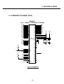
Figure. 3-3 SI4210 TRANSMITTER PART

3. TECHNICAL BRIEF
- 19 -
The Aero II transceiver can be configured in DCXO mode or VC-TCXO mode by the XMODE pin. To use
the transceiver in DCXO mode, the XMODE pin is tied high. The XTAL1 and XTAL2 pins are then
connected directly to the 26 MHz crystal. No additional components are required. The use of an external
VCTCXO module is also supported by tying the XMODE pin low. The VC-TCXO output should be input into
XTAL1, and XTAL2 should be tied low.
A buffer is available to provide a reference clock output from the XOUT pin to the baseband input. The
XOUT buffer is enabled when the XEN pin is set high, independent of the PDN pin. To achieve complete
powerdown during sleep, the XEN pin should be set low to disable the XOUT buffer. The XOUT buffer is
specified to drive a maximum load of 10 pF. The reference clock should be set to 13 MHz or 26 MHz by the
XDIV pin. When XDIV is tied low, XOUT is 26 MHz, and when it is tied high, XOUT is 13 MHz.
For a simple to follow methodology and detailed instructions on crystal selection, see "AN152: Selecting a
Crystal for Aero II Designs," or contact Silicon Laboratories Applications Support for assistance.
Figure. 3-4 DCXO BLOCK DIAGRAM

3. TECHNICAL BRIEF
- 20 -
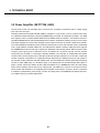
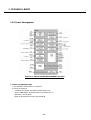
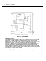
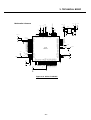
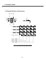
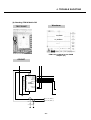
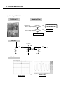
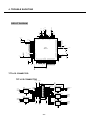
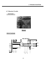
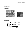
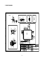
3.2 Power Amplifier (SKY77328, U400)
The RF parts consist of a transmitter part, a receiver part, a frequency synthesizer part, a voltage supply
part, and a VCTCXO part.
The SKY77328 Power Amplifier Module (PAM) is designed in a low profile (1.2 mm), compact form factor
for quad-band cellular handsets comprising GSM850/900, DCS1800, and PCS1900 operation. The PAM
also supports Class 12 General Packet Radio Service (GPRS) multi-slot operation. The module consists of
separate GSM850/900 PA and DCS1800/PCS1900 PA blocks, impedance-matching circuitry for 50 Ω input
and output impedances, and a Power Amplifier Control (PAC) block with an internal current-sense resistor.
The custom BiCMOS integrated circuit provides the internal PAC function and interface circuitry. Fabricated
onto a single Gallium Arsenide (GaAs) die, one Heterojunction Bipolar Transistor (HBT) PA block supports
the GSM850/900 bands and the other supports the DCS1800 and PCS1900 bands. Both PA blocks share
common power supply pins to distribute current. The GaAs die, the Silicon (Si) die, and the passive
components are mounted on a multi-layer laminate substrate. The assembly is encapsulated with plastic
overmold. RF input and output ports of the SKY77328 are internally matched to a 50 Ω load to reduce the
number of external components for a quad-band design. Extremely low leakage current (2.5 µA, typical) of
the dual PA module maximizes handset standby time. The SKY77328 also contains band-select switching
circuitry to select GSM (logic 0) or DCS/PCS (logic 1) as determined from the Band Select (BS) signal. In
Figure 1 below, the BS pin selects the PA output (DCS/PCS OUT or GSM850/900 OUT) and the Analog
Power Control (VAPC) controls the level of output power. The VBATT pin connects to an internal current-
sense resistor and interfaces to an integrated power amplifier control (iPAC™) function, which is insensitive
to variations in temperature, power supply, process, and input power. The ENABLE input allows initial turn-
on of PAM circuitry to minimize battery drain.

3. TECHNICAL BRIEF
- 21 -
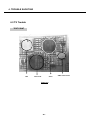
Figure. 3-5 SKY77328 FUNCTIONAL BLOCK DIAGRAM
Page is loading ...
Page is loading ...
Page is loading ...
Page is loading ...
Page is loading ...
Page is loading ...
Page is loading ...
Page is loading ...
Page is loading ...
Page is loading ...
Page is loading ...
Page is loading ...
Page is loading ...
Page is loading ...
Page is loading ...
Page is loading ...
Page is loading ...
Page is loading ...
Page is loading ...
Page is loading ...
Page is loading ...
Page is loading ...
Page is loading ...
Page is loading ...
Page is loading ...
Page is loading ...
Page is loading ...
Page is loading ...
Page is loading ...
Page is loading ...
Page is loading ...
Page is loading ...
Page is loading ...
Page is loading ...
Page is loading ...
Page is loading ...
Page is loading ...
Page is loading ...
Page is loading ...
Page is loading ...
Page is loading ...
Page is loading ...
Page is loading ...
Page is loading ...
Page is loading ...
Page is loading ...
Page is loading ...
Page is loading ...
Page is loading ...
Page is loading ...
Page is loading ...
Page is loading ...
Page is loading ...
Page is loading ...
Page is loading ...
Page is loading ...
Page is loading ...
Page is loading ...
Page is loading ...
Page is loading ...
Page is loading ...
Page is loading ...
Page is loading ...
Page is loading ...
Page is loading ...
Page is loading ...
Page is loading ...
Page is loading ...
Page is loading ...
Page is loading ...
Page is loading ...
Page is loading ...
Page is loading ...
Page is loading ...
Page is loading ...
Page is loading ...
Page is loading ...
Page is loading ...
Page is loading ...
Page is loading ...
Page is loading ...
Page is loading ...
Page is loading ...
Page is loading ...
Page is loading ...
Page is loading ...
Page is loading ...
Page is loading ...
Page is loading ...
Page is loading ...
Page is loading ...
Page is loading ...
Page is loading ...
Page is loading ...
Page is loading ...
Page is loading ...
Page is loading ...
Page is loading ...
Page is loading ...
Page is loading ...
Page is loading ...
Page is loading ...
Page is loading ...
Page is loading ...
Page is loading ...
Page is loading ...
Page is loading ...
Page is loading ...
Page is loading ...
Page is loading ...
Page is loading ...
Page is loading ...
Page is loading ...
Page is loading ...
Page is loading ...
Page is loading ...
Page is loading ...
Page is loading ...
Page is loading ...
Page is loading ...
Page is loading ...
Page is loading ...
Page is loading ...
Page is loading ...
Page is loading ...
Page is loading ...
Page is loading ...
Page is loading ...
-
 1
1
-
 2
2
-
 3
3
-
 4
4
-
 5
5
-
 6
6
-
 7
7
-
 8
8
-
 9
9
-
 10
10
-
 11
11
-
 12
12
-
 13
13
-
 14
14
-
 15
15
-
 16
16
-
 17
17
-
 18
18
-
 19
19
-
 20
20
-
 21
21
-
 22
22
-
 23
23
-
 24
24
-
 25
25
-
 26
26
-
 27
27
-
 28
28
-
 29
29
-
 30
30
-
 31
31
-
 32
32
-
 33
33
-
 34
34
-
 35
35
-
 36
36
-
 37
37
-
 38
38
-
 39
39
-
 40
40
-
 41
41
-
 42
42
-
 43
43
-
 44
44
-
 45
45
-
 46
46
-
 47
47
-
 48
48
-
 49
49
-
 50
50
-
 51
51
-
 52
52
-
 53
53
-
 54
54
-
 55
55
-
 56
56
-
 57
57
-
 58
58
-
 59
59
-
 60
60
-
 61
61
-
 62
62
-
 63
63
-
 64
64
-
 65
65
-
 66
66
-
 67
67
-
 68
68
-
 69
69
-
 70
70
-
 71
71
-
 72
72
-
 73
73
-
 74
74
-
 75
75
-
 76
76
-
 77
77
-
 78
78
-
 79
79
-
 80
80
-
 81
81
-
 82
82
-
 83
83
-
 84
84
-
 85
85
-
 86
86
-
 87
87
-
 88
88
-
 89
89
-
 90
90
-
 91
91
-
 92
92
-
 93
93
-
 94
94
-
 95
95
-
 96
96
-
 97
97
-
 98
98
-
 99
99
-
 100
100
-
 101
101
-
 102
102
-
 103
103
-
 104
104
-
 105
105
-
 106
106
-
 107
107
-
 108
108
-
 109
109
-
 110
110
-
 111
111
-
 112
112
-
 113
113
-
 114
114
-
 115
115
-
 116
116
-
 117
117
-
 118
118
-
 119
119
-
 120
120
-
 121
121
-
 122
122
-
 123
123
-
 124
124
-
 125
125
-
 126
126
-
 127
127
-
 128
128
-
 129
129
-
 130
130
-
 131
131
-
 132
132
-
 133
133
-
 134
134
-
 135
135
-
 136
136
-
 137
137
-
 138
138
-
 139
139
-
 140
140
-
 141
141
-
 142
142
-
 143
143
-
 144
144
-
 145
145
-
 146
146
-
 147
147
-
 148
148


