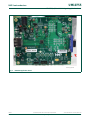
NXP PTN3393BS is a DisplayPort to LVDS interface bridge IC and a companion chip for PTN3360. It supports up to 2560x1600@60Hz WQXGA resolution with 24-bit color depth using either one or two LVDS channels. The PTN3393BS is a perfect fit for various applications such as mobile or desktop monitors and other embedded systems. PTN3393BS features:
- Compliant with VESA DisplayPort 1.2a specification
- Compliant with VESA Dual Mode DisplayPort (DP++) specification
- Supports up to 2560x1600@60Hz WQXGA resolution
- Supports 24-bit color depth
- Supports one or two LVDS channels
- Integrated HDCP 1.4 decrypter/repeater


-
 1
1
-
 2
2
-
 3
3
-
 4
4
-
 5
5
-
 6
6
-
 7
7
-
 8
8
-
 9
9
-
 10
10
-
 11
11
-
 12
12
-
 13
13
-
 14
14
-
 15
15
-
 16
16
-
 17
17
-
 18
18
-
 19
19


NXP PTN3393BS User guide
- Type
- User guide
- This manual is also suitable for
NXP PTN3393BS is a DisplayPort to LVDS interface bridge IC and a companion chip for PTN3360. It supports up to 2560x1600@60Hz WQXGA resolution with 24-bit color depth using either one or two LVDS channels. The PTN3393BS is a perfect fit for various applications such as mobile or desktop monitors and other embedded systems. PTN3393BS features:
- Compliant with VESA DisplayPort 1.2a specification
- Compliant with VESA Dual Mode DisplayPort (DP++) specification
- Supports up to 2560x1600@60Hz WQXGA resolution
- Supports 24-bit color depth
- Supports one or two LVDS channels
- Integrated HDCP 1.4 decrypter/repeater
Ask a question and I''ll find the answer in the document
Finding information in a document is now easier with AI
Related papers
Other documents
-
Thermo Scientific 4-20mA ULT Connection Operating instructions
-
 Koolance TMS-EB200 User manual
-
NXP Semiconductors JN5179 User manual
-
 AEG Powertools 8000011647 BAL User manual
-
 Sentera Controls HPD-G-1K0 Mounting Instruction
-
Texas Instruments DP-EXPANSION-EVM User Guides
-
Commell ADP-3355NB User manual
-
Microchip Technology SAMA5D27 SOM1 Kit1 User manual
-
-
Samsung SL-X7500LX Installation guide


