Silicon Labs C8051F700-DK User guide

Category
Network switches
Type
User guide

Silicon Labs C8051F700-DK is a development kit designed to help you evaluate and develop applications for the C8051F70x/71x MCU family. With a pre-soldered C8051F700 MCU, you can easily start developing your code using the included Silicon Laboratories IDE, which offers an integrated source-code editor, source-level debugger, and in-system programmer. The kit includes a USB debug adapter for easy programming and debugging, and an AC-to-DC universal power adapter and USB cables for convenient power and connectivity.

Silicon Labs C8051F700-DK is a development kit designed to help you evaluate and develop applications for the C8051F70x/71x MCU family. With a pre-soldered C8051F700 MCU, you can easily start developing your code using the included Silicon Laboratories IDE, which offers an integrated source-code editor, source-level debugger, and in-system programmer. The kit includes a USB debug adapter for easy programming and debugging, and an AC-to-DC universal power adapter and USB cables for convenient power and connectivity.

Rev. 0.3 8/13 Copyright © 2013 by Silicon Laboratories C8051F700-DK
C8051F700-DK
C8051F700 DEVELOPMENT KIT USERS GUIDE
1. Relevant Devices
The C8051F700 Development Kit is intended as a development platform for the microcontrollers in the
C8051F70x/71x MCU family. The members of this MCU family are: C8051F700, C8051F701, C8051F702,
C8051F703, C8051F704, C8051F705, C8051F706, C8051F707, C8051F708, C8051F709, C8051F710,
C8051F711, C8051F712, C8051F713, C8051F714, C8051F715.
The target board included in this kit is provided with a pre-soldered C8051F700 MCU.
Code developed on the C8051F700 can be easily ported to the other members of this MCU family.
Refer to the C8051F70x data sheet for the differences between the members of this MCU family.
2. Kit Contents
The C8051F700 Development Kit contains the following items:
C8051F700 Target Board
C8051Fxxx Development Kit Quick-Start Guide
Silicon Laboratories IDE and Product Information CD-ROM. CD content includes:
Silicon Laboratories Integrated Development Environment (IDE)
Evaluation assembler, compiler and linker tools
Source code examples and register definition files
Documentation
AC to DC universal power adapter
USB debug adapter
2 USB cables
3. Hardware Setup
Refer to Figure 1 for a diagram of the hardware configuration.
1. Connect the USB Debug Adapter to the DEBUG connector on the target board with the 10-pin ribbon cable.
2. Connect one end of the USB cable to the USB connector on the USB Debug Adapter.
3. Verify that shorting blocks are installed on the target board as shown in Figure 1.
4. Connect the other end of the USB cable to a USB Port on the PC.
5. Connect the ac/dc power adapter to power jack P2 on the target board.
Notes:
Use the Reset icon in the IDE to reset the target when connected during a debug session.
Remove power from the target board and the USB Debug Adapter before connecting or disconnecting the
ribbon cable from the target board. Connecting or disconnecting the cable when the devices have power can
damage the device and/or the USB Debug Adapter.
Not Recommended for New Designs
Downloaded from Arrow.com.
C8051F700-DK
2 Rev. 0.3
Figure 1. Hardware Setup using a USB Debug Adapter
Silicon Laboratories
USB DEBUG ADAPTER
Run
Stop Power
USB Debug Adapter
USB Cable
(To PC)
AC to DC Adapter
P4
DEBUG
P3
J17
J7
J11
J16
R8
SWITCH P2.3SWITCH P2.2
SWITCH P2.1SWITCH P2.0
RESET
POWER
P2
J8 DS3
P1.1
SW1
J2J1
J3
J0
J6
J12
J15
P1
F700
U1
J4J5 TB1
DS1
DS2
SW2
VDD
SILICON LABS
www.silabs.com
C8051F700-TB
J10J9
J13J14
Not Recommended for New Designs
Downloaded from Arrow.com.Downloaded from Arrow.com.
C8051F700-DK
Rev. 0.3 3
4. PC Software Overview
4.1. CP210x USB to UART VCP Driver Installation
The C8051F700 Target Board includes a Silicon Laboratories CP2102 USB-to-UART Bridge Controller (U2).
Device drivers for the CP2102 need to be installed before PC software such as HyperTerminal can communicate
with the target board over the USB connection. If the "Install CP210x Drivers" option is selected during installation,
a driver “unpacker” utility will launch.
1. Follow the steps to copy the driver files to the desired location. The default directory is C:\SiLabs\MCU\CP210x.
2. The final window will give an option to install the driver on the target system. Select the “Launch the CP210x VCP Driver
Installer” option if you are ready to install the driver.
3. If selected, the driver installer will now launch, providing an option to specify the driver installation location. After pressing
the “Install” button, the installer will search your system for copies of previously installed CP210x Virtual COM Port drivers. It
will let you know when your system is up to date. The driver files included in this installation have been certified by Microsoft.
4. If the “Launch the CP210x VCP Driver Installer” option was not selected in step 3, the installer can be found in the location
specified in step 2, by default C:\SiLabs\MCU\CP210x\Windows_2K_XP_S2K3_Vista. At this location run
CP210xVCPInstaller.exe.
5. To complete the installation process, connect the included USB cable between the host computer and the USB connector
(P4) on the C8051F700 Target Board. Windows will automatically finish the driver installation. Information windows will pop
up from the taskbar to show the installation progress.
If needed, the driver files can be uninstalled by selecting “Silicon Laboratories CP210x USB to UART Bridge (Driver Removal”
option in the “Add or Remove Programs” window.
4.2. Silicon Laboratories Integrated Development Environment
The Silicon Laboratories IDE integrates a source-code editor, source-level debugger and in-system programmer.
The use of third-party compilers, assemblers, and linkers is also supported. This development kit includes
evaluation versions of commercial C compilers and assemblers which can be used from within the Silicon
Laboratories IDE.
Not Recommended for New Designs
Downloaded from Arrow.com.Downloaded from Arrow.com.Downloaded from Arrow.com.
C8051F700-DK
4 Rev. 0.3
4.3. System Requirements
The Silicon Laboratories IDE requirements:
Pentium-class host PC running Windows 2000 or later.
One available USB port.
4.4. Third-Party Toolsets
The Silicon Laboratories IDE has native support for many 8051 compilers. Natively-supported tools are as follows:
Keil
IAR
Raisonance
Tasking
Hi-Tech
SDCC
Specific instructions for integrating each of the supported tools can be found in the application notes section of the
CD, or on the Silicon Labs web site (http://www.silabs.com).
4.5. Getting Started With the Silicon Labs IDE
The following sections discuss how to create a new project with the IDE, build the source code, and download it to
the target device.
4.5.1. Creating a New Project
1. Select ProjectNew Project to open a new project and reset all configuration settings to default.
2. Select FileNew File to open an editor window. Create your source file(s) and save the file(s) with a rec-
ognized extension, such as .c, .h, or .asm, to enable color syntax highlighting.
3. Right-click on “New Project” in the Project Window. Select Add files to project. Select files in the file
browser and click Open. Continue adding files until all project files have been added.
4. For each of the files in the
Project
Window
that you want assembled, compiled and linked into the target
build, right-click on the file name and select
Add file to build
. Each file will be assembled or compiled as
appropriate (based on file extension) and linked into the build of the absolute object file.
Note:
If a project contains a large number of files, the “Group” feature of the IDE can be used to organize.
Right-click on “New Project” in the
Project Window
. Select
Add Groups to project
. Add pre-defined
groups or add customized groups. Right-click on the group name and choose
Add file to group
. Select files
to be added. Continue adding files until all project files have been added.
4.5.2. Building and Downloading the Program for Debugging
1. Once all source files have been added to the target build, build the project by clicking on the Build/Make
Project button in the toolbar or selecting ProjectBuild/Make Project from the menu.
Note: After the project has been built the first time, the Build/Make Project command will only build the
files that have been changed since the previous build. To rebuild all files and project dependencies, click
on the Rebuild All button in the toolbar or select ProjectRebuild All from the menu.
2.
Before connecting to the target device, several connection options may need to be set.
Open the
Connection Options
window by selecting
Options
Connection Options...
in the IDE menu. First, select
the “USB Debug Adapter” option. Next, the correct “Debug Interface” must be selected.
C8051F700
devices
use Silicon Labs “
C2
” 2-wire debug interface. Once all the selections are made, click the
OK
button to close
the window.
3. Click the
Connect
button in the toolbar or select
Debug
Connect
from the menu to connect to the device.
4. Download the project to the target by clicking the Download Code button in the toolbar.
Not Recommended for New Designs
Downloaded from Arrow.com.Downloaded from Arrow.com.Downloaded from Arrow.com.Downloaded from Arrow.com.
C8051F700-DK
Rev. 0.3 5
Note: To enable automatic downloading if the program build is successful select Enable automatic con-
nect/download after build in the ProjectTarget Build Configuration dialog. If errors occur during the
build process, the IDE will not attempt the download.
5. Save the project when finished with the debug session to preserve the current target build configuration,
editor settings and the location of all open debug views. To save the project, select ProjectSave Project
As... from the menu. Create a new name for the project and click on Save.
5. Example Source Code
Example source code and register definition files are provided in the “SiLabs\MCU\Examples\C8051F70x_71x\
directory during IDE installation. These files may be used as a template for code development. The comments in
each example file indicate which development tool chains were used when testing.
5.1. Register Definition Files
Register definition files C8051F70x.inc, C8051F70x_defs.h and compiler_defs.h define all SFR registers and bit-
addressable control/status bits. They are installed into the “SiLabs\MCU\Examples\C8051F70x_71x\” directory
during IDE installation. The register and bit names are identical to those used in the C8051F70x datasheet.
5.2. Blinking LED Example
The example source files F70x_Blinky.asm and F70x_Blinky.c installed in the default directory
“SiLabs\MCU\Examples\C8051F70x_71x\Blinky” show examples of several basic C8051F700 functions. These
include disabling the watchdog timer (WDT), configuring the Port I/O crossbar, configuring a timer for an interrupt
routine, initializing the system clock, and configuring a GPIO port pin. When compiled/assembled and linked this
program flashes the green LED (DS3) on the C8051F700 Target Board about five times a second using the
interrupt handler with a C8051F700 timer.
5.3. Capacitive Sense Switch Example
The example source file F70x_CS0.c demonstrates the configuration and usage of the capacitive sense switches
located on P2.0 through P2.3. Refer to the source file for step-by-step instructions to build and test this example.
This is installed in the “SiLabs\MCU\Examples\C8051F70x_71x\ CS0\” directory by default.
Not Recommended for New Designs
Downloaded from Arrow.com.Downloaded from Arrow.com.Downloaded from Arrow.com.Downloaded from Arrow.com.Downloaded from Arrow.com.
C8051F700-DK
6 Rev. 0.3
6. Target Board
The C8051F700 Development Kit includes a target board with a C8051F700 device pre-installed for evaluation and
preliminary software development. Numerous input/output (I/O) connections are provided to facilitate prototyping
using the target board. Refer to Figure 2 for the locations of the various I/O connectors. Figure 2 shows the factory
default shorting block positions.
DS1 LED indicates that the USB connection is providing power to the USB to UART device U2
DS2 LED indicates whether power is being supplied through selection made on J15
DS3 LED connects to P1.0 through J8
P1 Expansion connector (96-pin)
P2 Power connector (accepts input from 7 to 15 VDC unregulated power adapter)
P3 DEBUG connector for Debug Adapter interface
P4 USB connector (connects to PC for serial communication)
J0 - J6 Port I/O headers (provide access to Port I/O pins)
J7 Provides easily accessible ground clip
J8 Connects P1.0 to LED DS3 and P1.1 to switch SW1
J9 Connects P0.2 (XTAL1) to one terminal of Y1
J10 Connects P0.3 (XTAL2) to one terminal of Y1
J11 Selects either on-board regulator or USB debug adapter as VDD_LDO power source
J12 Connects port I/O to the UART0 interface
J13 Connects P0.0/VREF to bypass capacitor
J14 Connects P0.1/AGND to GND
J15 Selects one of the available power sources as the board supply
J16 Connects P1.2 to potentiometer R8
SW1 Switch connected to the MCU I/O pin P1.1
SW2 Switch connected to the reset pin of the MCU
TB1 Analog I/O terminal block
Not Recommended for New Designs
Downloaded from Arrow.com.Downloaded from Arrow.com.Downloaded from Arrow.com.Downloaded from Arrow.com.Downloaded from Arrow.com.Downloaded from Arrow.com.
C8051F700-DK
Rev. 0.3 7
Figure 2. C8051F700 Target Board
P4
DEBUG
P3
J17
J7
J11
J16
R8
SWITCH P2.3SWITCH P2.2
SWITCH P2.1SWITCH P2.0
RESET
POWER
P2
J8 DS3
P1.1
SW1
J2J1
J3
J0
J6
J12
J15
P1
F700
U1
J4J5 TB1
DS1
DS2
SW2
VDD
SILICON LABS
www.silabs.com
C8051F700-TB
J10J9
J13J14
Pin 1
Not Recommended for New Designs
Downloaded from Arrow.com.Downloaded from Arrow.com.Downloaded from Arrow.com.Downloaded from Arrow.com.Downloaded from Arrow.com.Downloaded from Arrow.com.Downloaded from Arrow.com.
C8051F700-DK
8 Rev. 0.3
6.1. Target Board Shorting Blocks: Factory Defaults
The C8051F700 target board comes from the factory with pre-installed shorting blocks on many headers. Figure 3
shows the positions of the factory default shorting blocks.
Figure 3. C8051F700 Target Board Shorting Blocks: Factory Defaults
P4
DEBUG
P3
J17
J7
J11
J16
R8
SWITCH P2.3SWITCH P2.2
SWITCH P2.1SWITCH P2.0
RESET
POWER
P2
J8 DS3
P1.1
SW1
J2J1
J3
J0
J6
J12
J15
P1
F700
U1
J4J5 TB1
DS1
DS2
SW2
VDD
SILICON LABS
www.silabs.com
C8051F700-TB
J10J9
J13J14
Not Recommended for New Designs
Downloaded from Arrow.com.Downloaded from Arrow.com.Downloaded from Arrow.com.Downloaded from Arrow.com.Downloaded from Arrow.com.Downloaded from Arrow.com.Downloaded from Arrow.com.Downloaded from Arrow.com.
C8051F700-DK
Rev. 0.3 9
6.2. Target Board Power Options and Current Measurement
The C8051F700 Target Board supports three power options, selectable by placing a shorting block on J15. The
power options are described in the paragraphs below.
6.2.1. Wall Power and Debug Power
Placing a shorting block on J15 that connects VDD_LDO to VDD configures the board to be powered from the
output of the on-board regulator to power the device.
Place a shorting block on J3 between pins 2 and 3 in order to route supply from power jack P2 into the on-board
LDO.
Place a shorting block on J3 between pins 1 and 2 in order to route supply from the debug adapter (P3) into the on-
board LDO.
6.2.2. External Supply
Placing a shorting block on J15 that connects VDD_EXT to VDD configures the board to be powered from a
voltage connected to the VDD_EXT input of TB1.
6.2.3. USB Power
Placing a shorting block on J15 that connects VDD_USB to VDD configures the board to be powered from the
output of U2’s on-chip regulator.
J15
J11
Pin 1
J11
Pin 1
J15
J15
Not Recommended for New Designs
Downloaded from Arrow.com.Downloaded from Arrow.com.Downloaded from Arrow.com.Downloaded from Arrow.com.Downloaded from Arrow.com.Downloaded from Arrow.com.Downloaded from Arrow.com.Downloaded from Arrow.com.Downloaded from Arrow.com.
C8051F700-DK
10 Rev. 0.3
6.3. System Clock Sources
6.3.1. Internal Oscillator
The C8051F700 devices feature a calibrated internal oscillator which is enabled as the system clock source on
reset. After reset, the internal oscillator operates at a frequency of 24.5 MHz (±2%) by default, but may be
configured by software to operate at other frequencies. Therefore, in many applications an external oscillator is not
required. However, if you wish to operate the C8051F700 device at a frequency not available with the internal
oscillator, an external oscillator source may be used. Refer to the C8051F70x datasheet for more information on
configuring the system clock source.
6.3.2. External Oscillator Options
The main board is designed to facilitate the use of external clock sources. To use an external CMOS clock source,
the clock can simply be applied to P0.3. For RC and C modes, place a shorting block on header J10. To implement
the RC mode option, placeholders for an 0805-packaged capacitor (C17) and resistor (R14) are supplied on the
board. The C (capacitor) clock option can be implemented by using only the capacitor placeholder (C17). To
reduce the amount of stray capacitance on the pin, which could affect the frequency in either RC or C mode,
resistor R13 can also be removed from the board when using C or RC mode. To implement external crystal mode,
place shorting blocks at headers J9 and J10 and install the crystal at the pads marked Y1. Install a 10 M resistor
at R13 and install capacitors at C17 and C18 using values appropriate for the crystal you select. Refer to the
C8051F700 datasheet for more information on the use of external oscillators.
6.4. Switches and LEDs
Two push-button switches are provided on the main board. Switch RESET is connected to the RESET pin of the
C8051F700. Pressing RESET puts the device into its hardware-reset state. Switch SW1 P1.1 can be connected to
the C8051F700’s general purpose I/O (GPIO) pin P1.0 through header J8. Pressing Switch SW1 P1.1 generates a
logic low signal on the port pin. Remove the shorting block from the J8 header to disconnect Switch SW1 P1.1 from
the port pin.
Four capacitive sense switches are provided on the target board. The operation of these switches require
appropriate firmware running on the C8051F700 MCU that can sense the state of the switch. See Section "5.3.
Capacitive Sense Switch Example" on page 5 for details about example source code.
Three LEDs are also provided on the target board. The red LED labeled USB PWR (DS1) is used to indicate a USB
connection to P4. The red LED labeled DS2 indicates when power is being applied to the board through J15.
Finally, the green LED labeled P1.0 (DS2) can be connected to the C8051F700’s GPIO pin P1.0 through header
J8. Remove the shorting block from the header to disconnect the LED from the port pin.
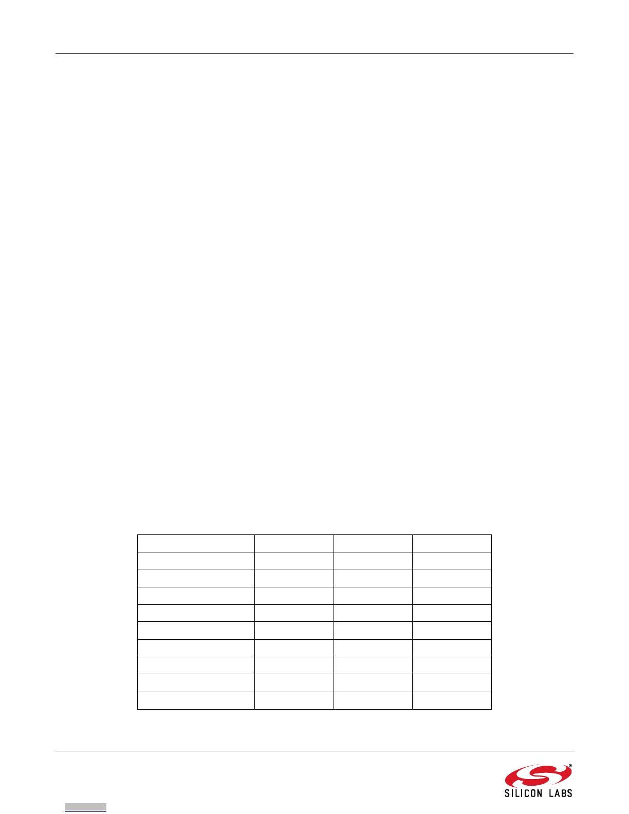
See Table 1 for the port pins and headers corresponding to the switches and LEDs.
Table 1. Target Board I/O Descriptions
Description Label I/O Header
Push-button Switch SW1 P1.1 J8
Push-button Switch SW2 RESET none
Capacitive Sense Switch C1 P2.0 none
Capacitive Sense Switch C2 P2.1 none
Capacitive Sense Switch C3 P2.2 none
Capacitive Sense Switch C4 P2.3 none
Green LED DS3 P1.0 J8
Red LED DS2 VDD none
Red LED DS1 5V_VBUS none
Not Recommended for New Designs
Downloaded from Arrow.com.Downloaded from Arrow.com.Downloaded from Arrow.com.Downloaded from Arrow.com.Downloaded from Arrow.com.Downloaded from Arrow.com.Downloaded from Arrow.com.Downloaded from Arrow.com.Downloaded from Arrow.com.Downloaded from Arrow.com.
C8051F700-DK
Rev. 0.3 11
6.5. Target Board DEBUG Interface (DEBUG / P3)
The DEBUG connector J9 provides access to the DEBUG (C2) pins of the C8051F700. It is used to connect the
Serial Adapter or the USB Debug Adapter to the target board for in-circuit debugging and Flash programming.
Table 2 shows the DEBUG pin definitions.
Table 2. Debug Connector (P3) Description
6.6. Port I/O Connectors (J0-J6)
Each of the parallel ports of the C8051F700 has its own 10-pin header connector. Each connector provides a pin
for the corresponding port pins 0-7, VDD, and digital ground. The same pin-out is used for all of the port
connectors, and is shown in Table 3 .
6.7. Serial Interface (P4)
A USB-to-UART bridge circuit (U2) and USB connector (P4) are provided on the target board to facilitate serial
connections to UART0 of the C8051F700. The Silicon Labs CP2103 USB-to-UART bridge provides data
connectivity between the C8051F700 and the PC via a USB port. The TX and RX signals of UART0 may be
connected to the CP2102 by installing shorting blocks on header J17. The shorting block between VDD and VIO on
header J12[1-2] is required when using this interface. Optionally, firmware can use I/O pins for hardware
handshaking (/RTS and /CTS). The shorting block positions for connecting each of these signals to the CP2103
are listed in Table 4. To use this interface, the USB-to-UART device drivers should be installed as described in
Section "4.1. CP210x USB to UART VCP Driver Installation" on page 3.
Pin # Description
1 VDD_F700 (+3.3 VDC)
2, 3, 9 GND (Ground)
4C2D
5 /RST (Reset)
6 Not connected
7 /RST/C2CK
8 Not connected
10 USB Power (+5 VDC)
Table 3. Port I/O Connector Pin Description
Pin # Pin Description
1Pn.0
2Pn.1
3Pn.2
4Pn.3
5Pn.4
6Pn.5
7Pn.6
8Pn.7
9 VDD (VDD_F700)
10 GND (Ground)
Not Recommended for New Designs
Downloaded from Arrow.com.Downloaded from Arrow.com.Downloaded from Arrow.com.Downloaded from Arrow.com.Downloaded from Arrow.com.Downloaded from Arrow.com.Downloaded from Arrow.com.Downloaded from Arrow.com.Downloaded from Arrow.com.Downloaded from Arrow.com.Downloaded from Arrow.com.
C8051F700-DK
12 Rev. 0.3
6.8. Voltage Reference (VREF) and Analog Ground Connectors (J13 and J14)
The VREF connector can be used to connect the VREF pin from the MCU (P0.0) to external 0.1 uF and 4.7 uF
decoupling capacitors. The C8051F700 device is connected to the capacitors through the J13 header. The AGND
pin from the MCU (P0.1) can be connected to the board digital ground through the J14 header.
6.9. Potentiometer (J16)
The C8051F700 device has the option to connect port pin P1.2 to a 10 k linear potentiometer. The potentiometer
is connected through the J16 header. The potentiometer can be used for testing the analog-to-digital (ADC)
converter of the MCU.
6.10. C2 Pin Sharing
On the C8051F700, the debug pin C2CK is shared with the /RST pin. The target board includes the resistor
necessary to enable pin sharing which allows the pin–shared /RST to be used normally while simultaneously
debugging the device. See Application Note “AN124: Pin Sharing Techniques for the C2 Interface” at
www.silabs.com for more information regarding pin sharing.
Table 4. Serial Interface Header (J12) Description
Header Pins MCU I/O Pin CP2103 Pin
J12[1-2] none Board VDD to CP2103 VIO
J12[3-4] P0.5 TXD
J12[5-6] P0.4 RXD
J12[7-8] P0.6 /RTS
J12[9-10] P0.7 /CTS
Not Recommended for New Designs
Downloaded from Arrow.com.Downloaded from Arrow.com.Downloaded from Arrow.com.Downloaded from Arrow.com.Downloaded from Arrow.com.Downloaded from Arrow.com.Downloaded from Arrow.com.Downloaded from Arrow.com.Downloaded from Arrow.com.Downloaded from Arrow.com.Downloaded from Arrow.com.Downloaded from Arrow.com.
C8051F700-DK
Rev. 0.3 13
6.11. Expansion Connector (P1)
The 96-pin expansion I/O connector P1 is used to connect daughter boards to the main target board. P1 provides
access to all of the C8051F700 pins. Pins for VDD and GND are also available. See Table 5 for a complete list of
pins available at P1.
The P1 socket connector is manufactured by Hirose Electronic Co. Ltd, part number PCN13-96S-2.54DS, Digi-Key
part number H7096-ND. The corresponding plug connector is also manufactured by Hirose Electronic Co. Ltd, part
number PCN10-96P-2.54DS, Digi-Key part number H5096-ND.
Table 5. P1 Pin Listing
Pin # Description Pin # Description Pin # Description
A-1 VDD_F700 B-1 GND C-1 N/C
A-2 N/C B-2 N/C C-2 N/C
A-3 N/C B-3 N/C C-3 N/C
A-4 N/C B-4 N/C C-4 N/C
A-5 P2.7 B-5 P2.6 C-5 P2.5
A-6 P2.4 B-6 P2.3 C-6 P2.2
A-7 P2.1 B-7 P2.0 C-7 P1.7
A-8 P1.6 B-8 P1.5 C-8 P1.4
A-9 P1.3 B-9 P1.2 C-9 P1.1
A-10 P1.0 B-10 P0.7 C-10 P0.6
A-11 P0.5 B-11 P0.4 C-11 P0.3
A-12 P0.2 B-12 P0.1 C-12 P0.0
A-13 P5.7 B-13 P5.6 C-13 P5.5
A-14 P5.4 B-14 P5.3 C-14 P5.2
A-15 P5.1 B-15 P5.0 C-15 P4.7
A-16 P4.6 B-16 P4.5 C-16 P4.4
A-17 P4.3 B-17 P4.2 C-17 P4.1
A-18 P4.0 B-18 P3.7 C-18 P3.6
A-19 P3.5 B-19 P3.4 C-19 P3.3
A-20 P3.2 B-20 P3.1 C-20 P3.0
A-21 P6.0 B-21 P6.1 C-21 P6.2
A-22 P6.3 B-22 P6.4 C-22 P6.5
A-23 N/C B-23 N/C C-23 N/C
A-24 C2D B-24 N/C C-24 N/C
A-25 RST/C2CK B-25 GND C-25 N/C
A-26 GND B-26 N/C C-26 N/C
A-27 N/C B-27 N/C C-27 N/C
A-28 N/C B-28 VDD_F700 C-28 N/C
A-29 N/C B-29 N/C C-29 N/C
A-30 N/C B-30 N/C C-30 N/C
A-31 N/C B-31 N/C C-31 N/C
A-32 N/C B-32 GND C-32 N/C
Not Recommended for New Designs
Downloaded from Arrow.com.Downloaded from Arrow.com.Downloaded from Arrow.com.Downloaded from Arrow.com.Downloaded from Arrow.com.Downloaded from Arrow.com.Downloaded from Arrow.com.Downloaded from Arrow.com.Downloaded from Arrow.com.Downloaded from Arrow.com.Downloaded from Arrow.com.Downloaded from Arrow.com.Downloaded from Arrow.com.
C8051F700-DK
14 Rev. 0.3
7. Schematics
Figure 4. C8051F700 Target Board Schematic (Page 1 of 3)
Not Recommended for New Designs
Downloaded from Arrow.com.Downloaded from Arrow.com.Downloaded from Arrow.com.Downloaded from Arrow.com.Downloaded from Arrow.com.Downloaded from Arrow.com.Downloaded from Arrow.com.Downloaded from Arrow.com.Downloaded from Arrow.com.Downloaded from Arrow.com.Downloaded from Arrow.com.Downloaded from Arrow.com.Downloaded from Arrow.com.Downloaded from Arrow.com.
C8051F700-DK
Rev. 0.3 15
Figure 5. C8051F700 Target Board Schematic (Page 2 of 3)
Not Recommended for New Designs
Downloaded from Arrow.com.Downloaded from Arrow.com.Downloaded from Arrow.com.Downloaded from Arrow.com.Downloaded from Arrow.com.Downloaded from Arrow.com.Downloaded from Arrow.com.Downloaded from Arrow.com.Downloaded from Arrow.com.Downloaded from Arrow.com.Downloaded from Arrow.com.Downloaded from Arrow.com.Downloaded from Arrow.com.Downloaded from Arrow.com.Downloaded from Arrow.com.
C8051F700-DK
16 Rev. 0.3
Figure 6. C8051F700 Target Board Schematic (Page 3 of 3)
Not Recommended for New Designs
Downloaded from Arrow.com.Downloaded from Arrow.com.Downloaded from Arrow.com.Downloaded from Arrow.com.Downloaded from Arrow.com.Downloaded from Arrow.com.Downloaded from Arrow.com.Downloaded from Arrow.com.Downloaded from Arrow.com.Downloaded from Arrow.com.Downloaded from Arrow.com.Downloaded from Arrow.com.Downloaded from Arrow.com.Downloaded from Arrow.com.Downloaded from Arrow.com.Downloaded from Arrow.com.
C8051F700-DK
Rev. 0.3 17
DOCUMENT CHANGE LIST
Revision 0.2 to Revision 0.3
Removed QuickSense references.
Not Recommended for New Designs
Downloaded from Arrow.com.Downloaded from Arrow.com.Downloaded from Arrow.com.Downloaded from Arrow.com.Downloaded from Arrow.com.Downloaded from Arrow.com.Downloaded from Arrow.com.Downloaded from Arrow.com.Downloaded from Arrow.com.Downloaded from Arrow.com.Downloaded from Arrow.com.Downloaded from Arrow.com.Downloaded from Arrow.com.Downloaded from Arrow.com.Downloaded from Arrow.com.Downloaded from Arrow.com.Downloaded from Arrow.com.
Disclaimer
Silicon Laboratories intends to provide customers with the latest, accurate, and in-depth documentation of all peripherals and modules available for system and software implementers
using or intending to use the Silicon Laboratories products. Characterization data, available modules and peripherals, memory sizes and memory addresses refer to each specific
device, and "Typical" parameters provided can and do vary in different applications. Application examples described herein are for illustrative purposes only. Silicon Laboratories
reserves the right to make changes without further notice and limitation to product information, specifications, and descriptions herein, and does not give warranties as to the accuracy
or completeness of the included information. Silicon Laboratories shall have no liability for the consequences of use of the information supplied herein. This document does not imply
or express copyright licenses granted hereunder to design or fabricate any integrated circuits. The products must not be used within any Life Support System without the specific
written consent of Silicon Laboratories. A "Life Support System" is any product or system intended to support or sustain life and/or health, which, if it fails, can be reasonably expected
to result in significant personal injury or death. Silicon Laboratories products are generally not intended for military applications. Silicon Laboratories products shall under no
circumstances be used in weapons of mass destruction including (but not limited to) nuclear, biological or chemical weapons, or missiles capable of delivering such weapons.
Trademark Information
Silicon Laboratories Inc., Silicon Laboratories, Silicon Labs, SiLabs and the Silicon Labs logo, CMEMS®, EFM, EFM32, EFR, Energy Micro, Energy Micro logo and combinations
thereof, "the world’s most energy friendly microcontrollers", Ember®, EZLink®, EZMac®, EZRadio®, EZRadioPRO®, DSPLL®, ISOmodem ®, Precision32®, ProSLIC®, SiPHY®,
USBXpress® and others are trademarks or registered trademarks of Silicon Laboratories Inc. ARM, CORTEX, Cortex-M3 and THUMB are trademarks or registered trademarks of
ARM Holdings. Keil is a registered trademark of ARM Limited. All other products or brand names mentioned herein are trademarks of their respective holders.
http://www.silabs.com
Silicon Laboratories Inc.
400 West Cesar Chavez
Austin, TX 78701
USA
Simplicity Studio
One-click access to MCU and
wireless tools, documentation,
software, source code libraries &
more. Available for Windows,
Mac and Linux!
IoT Portfolio
www.silabs.com/IoT SW/HW
www.silabs.com/simplicity Quality
www.silabs.com/quality Support and Community
community.silabs.com
Not Recommended for New Designs
Downloaded from Arrow.com.Downloaded from Arrow.com.Downloaded from Arrow.com.Downloaded from Arrow.com.Downloaded from Arrow.com.Downloaded from Arrow.com.Downloaded from Arrow.com.Downloaded from Arrow.com.Downloaded from Arrow.com.Downloaded from Arrow.com.Downloaded from Arrow.com.Downloaded from Arrow.com.Downloaded from Arrow.com.Downloaded from Arrow.com.Downloaded from Arrow.com.Downloaded from Arrow.com.Downloaded from Arrow.com.Downloaded from Arrow.com.
  • Page 1 1
  • Page 2 2
  • Page 3 3
  • Page 4 4
  • Page 5 5
  • Page 6 6
  • Page 7 7
  • Page 8 8
  • Page 9 9
  • Page 10 10
  • Page 11 11
  • Page 12 12
  • Page 13 13
  • Page 14 14
  • Page 15 15
  • Page 16 16
  • Page 17 17
  • Page 18 18

Silicon Labs C8051F700-DK User guide

Category
Network switches
Type
User guide

Silicon Labs C8051F700-DK is a development kit designed to help you evaluate and develop applications for the C8051F70x/71x MCU family. With a pre-soldered C8051F700 MCU, you can easily start developing your code using the included Silicon Laboratories IDE, which offers an integrated source-code editor, source-level debugger, and in-system programmer. The kit includes a USB debug adapter for easy programming and debugging, and an AC-to-DC universal power adapter and USB cables for convenient power and connectivity.

Ask a question and I''ll find the answer in the document

Finding information in a document is now easier with AI