
CY7B991
CY7B992
Programmable Skew Clock Buffer
Cypress Semiconductor Corporation • 198 Champion Court • San Jose, CA 95134-1709 • 408-943-2600
Document Number: 38-07138 Rev. *B Revised June 22, 2007
Features
■ All output pair skew <100 ps typical (250 maximum)
■ 3.75 to 80 MHz output operation
■ User selectable output functions
❐ Selectable skew to 18 ns
❐ Inverted and non-inverted
❐ Operation at 1⁄2 and 1⁄4 input frequency
❐ Operation at 2x and 4x input frequency (input as low as 3.75
MHz)
■ Zero input to output delay
■ 50% duty cycle outputs
■ Outputs drive 50Ω terminated lines
■ Low operating current
■ 32-pin PLCC/LCC package
■ Jitter < 200 ps peak-to-peak (< 25 ps RMS)
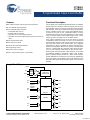
Functional Description
The CY7B991 and CY7B992 Programmable Skew Clock Buffers
(PSCB) offer user selectable control over system clock functions.
These multiple output clock drivers provide the system integrator
with functions necessary to optimize the timing of high perfor-
mance computer systems. Each of the eight individual drivers,
arranged in four pairs of user controllable outputs, can drive
terminated transmission lines with impedances as low as 50Ω.
They can deliver minimal and specified output skews and full
swing logic levels (CY7B991 TTL or CY7B992 CMOS).
Each output is hardwired to one of the nine delay or function
configurations. Delay increments of 0.7 to 1.5 ns are determined
by the operating frequency with outputs that skew up to ±6 time
units from their nominal “zero” skew position. The completely
integrated PLL allows cancellation of external load and trans-
mission line delay effects. When this “zero delay” capability of the
PSCB is combined with the selectable output skew functions,
you can create output-to-output delays of up to ±12 time units.
Divide-by-two and divide-by-four output functions are provided
for additional flexibility in designing complex clock systems.
When combined with the internal PLL, these divide functions
enable distribution of a low frequency clock that are multiplied by
two or four at the clock destination. This facility minimizes clock
distribution difficulty, allowing maximum system clock speed and
flexibility.
Logic Block Diagram
TEST
FB
REF
VCO AND
TIME UNIT
GENERATOR
FS
SELECT
INPUTS
(THREE
LEVEL)
SKEW
SELECT
MATRIX
4F0
4F1
3F0
3F1
2F0
2F1
1F0
1F1
4Q0
4Q1
3Q0
3Q1
2Q0
2Q1
1Q0
1Q1
FILTER
PHASE
FREQ
DET
[+] Feedback

CY7B991
CY7B992
Document Number: 38-07138 Rev. *B Page 2 of 19
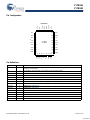
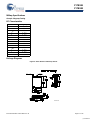
Pin Configuration
Pin Definitions
Signal Name IO Description
REF I Reference frequency input. This input supplies the frequency and timing against which all functional
variations are measured.
FB I PLL feedback input (typically connected to one of the eight outputs).
FS I Three level frequency range select. See Table 1.
1F0, 1F1 I Three level function select inputs for output pair 1 (1Q0, 1Q1). See Table 2.
2F0, 2F1 I Three level function select inputs for output pair 2 (2Q0, 2Q1). See Table 2.
3F0, 3F1 I Three level function select inputs for output pair 3 (3Q0, 3Q1). See Table 2.
4F0, 4F1 I Three level function select inputs for output pair 4 (4Q0, 4Q1). See Table 2.
TEST I Three level select. See “Test Mode” on page 4 under the “Block Diagram Description” on page 3.
1Q0, 1Q1 O Output pair 1. See Table 2.
2Q0, 2Q1 O Output pair 2. See Table 2.
3Q0, 3Q1 O Output pair 3. See Table 2.
4Q0, 4Q1 O Output pair 4. See Table 2.
V
CCN
PWR Power supply for output drivers.
V
CCQ
PWR Power supply for internal circuitry.
GND PWR Ground.
1234323130
17161514 18 19 20
5
6
7
8
9
10
11
12
13
29
28
27
26
25
24
23
22
21
3F0
FS
V
REF
GND
TEST
2F1
FB
2Q1
2Q0
CCQ
2F0
GND
1F1
1F0
V
CCN
1Q0
1Q1
GND
GND
3Q1
3Q0
CCN
V
CCN
V
3F1
4F0
4F1
V
CCQ
V
CCN
4Q1
4Q0
GND
GND
PLCC/LCC
CY7B991
CY7B992
[+] Feedback

CY7B991
CY7B992
Document Number: 38-07138 Rev. *B Page 3 of 19
Block Diagram Description
Phase Frequency Detector and Filter
The Phase Frequency Detector and Filter blocks accept inputs
from the reference frequency (REF) input and the feedback (FB)
input and generate correction information to control the
frequency of the Voltage Controlled Oscillator (VCO). These
blocks, along with the VCO, form a Phase Locked Loop (PLL)
that tracks the incoming REF signal.
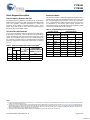
VCO and Time Unit Generator
The VCO accepts analog control inputs from the PLL filter block.
It generates a frequency used by the time unit generator to
create discrete time units that are selected in the skew select
matrix. The operational range of the VCO is determined by the
FS control pin. The time unit (t
U
) is determined by the operating
frequency of the device and the level of the FS pin as shown in
Table 1.
Skew Select Matrix
The skew select matrix contains four independent sections. Each
section has two low skew, high fanout drivers (xQ0, xQ1), and
two corresponding three level function select (xF0, xF1) inputs.
Table 2 shows the nine possible output functions for each section
as determined by the function select inputs. All times are
measured with respect to the REF input assuming that the output
connected to the FB input has 0t
U
selected.
Table 1. Frequency Range Select and t
U
Calculation
[1]
FS
[2, 3]
f
NOM
(MHz)
where N =
Approximate
Frequency (MHz) At
Which t
U
= 1.0 ns
Min Max
LOW 15 30 44 22.7
MID 25 50 26 38.5
HIGH 40 80 16 62.5
t
U
1
f
NOM
N×
------------------------
=
Table 2. Programmable Skew Configurations
[1]
Function Selects Output Functions
1F1, 2F1,
3F1, 4F1
1F0, 2F0,
3F0, 4F0
1Q0, 1Q1,
2Q0, 2Q1
3Q0, 3Q1 4Q0, 4Q1
LOW LOW –4t
U
Divide by 2 Divide by 2
LOW MID –3t
U
–6t
U
–6t
U
LOW HIGH –2t
U
–4t
U
–4t
U
MID LOW –1t
U
–2t
U
–2t
U
MID MID 0t
U
0t
U
0t
U
MID HIGH +1t
U
+2t
U
+2t
U
HIGH LOW +2t
U
+4t
U
+4t
U
HIGH MID +3t
U
+6t
U
+6t
U
HIGH HIGH +4t
U
Divide by 4 Inverted
Notes
1. For all tri-state inputs, HIGH indicates a connection to VCC, LOW indicates a connection to GND, and MID indicates an open connection. Internal termination circuitry
holds an unconnected input to VCC/2.
2. The level is set on FS is determined by the “normal” operating frequency (fNOM) of the VCO and Time Unit Generator (see Logic Block Diagram). Nominal frequency
(fNOM) always appears at 1Q0 and the other outputs when they are operated in their undivided modes (see Tab le 2). The frequency appearing at the REF and FB
inputs are fNOM when the output connected to FB is undivided. The frequency of the REF and FB inputs are fNOM/2 or fNOM/4 when the part is configured for a
frequency multiplication by using a divided output as the FB input.
3. When the FS pin is selected HIGH, the REF input must not transition upon power up until VCC has reached 4.3V.
[+] Feedback

CY7B991
CY7B992
Document Number: 38-07138 Rev. *B Page 4 of 19
Test Mode
The TEST input is a three level input. In normal system
operation, this pin is connected to ground, enabling the
CY7B991 or CY7B992 to operate as explained in “Skew Select
Matrix” on page 3. For testing purposes, any of the three level
inputs can have a removable jumper to ground, or be tied LOW
through a 100Ω resistor. This enables an external tester to
change the state of these pins.
If the TEST input is forced to its MID or HIGH state, the device
operates with its internal phase locked loop disconnected, and
input levels supplied to REF directly controls all outputs. Relative
output to output functions are the same as in normal mode.
In contrast with normal operation (TEST tied LOW), all outputs
function based only on the connection of their own function
selects inputs (xF0 and xF1) and the waveform characteristics of
the REF input.
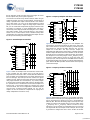
Figure 1 shows the typical outputs with FB connected to a zero skew output.
[4]
Figure 1. Typical Outputs with FB Connected to a Zero-Skew Output
t
0
– 6t
U
t
0
– 5t
U
t
0
– 4t
U
t
0
– 3t
U
t
0
– 2t
U
t
0
– 1t
U
t
0
t
0
+1t
U
t
0
t
0
t
0
t
0
t
0
+2t
U
+3t
U
+4t
U
+5t
U
+6t
U
FBInput
REFInput
– 6t
U
– 4t
U
– 3t
U
– 2t
U
– 1t
U
0t
U
+1t
U
+2t
U
+3t
U
+4t
U
+6t
U
DIVIDED
INVERT
LM
LH
(N/A)
ML
(N/A)
MM
(N/A)
MH
(N/A)
HL
HM
LL/HH
HH
3Fx
4Fx
(N/A)
LL
LM
LH
ML
MM
MH
HL
HM
HH
(N/A)
(N/A)
(N/A)
1Fx
2Fx
Note
4. FB connected to an output selected for “zero” skew (i.e., xF1 = xF0 = MID).
[+] Feedback

CY7B991
CY7B992
Document Number: 38-07138 Rev. *B Page 5 of 19
Maximum Ratings
Operating outside these boundaries affects the performance and
life of the device. These user guidelines are not tested.
Storage Temperature .................................–65
°C to +150°C
Ambient Temperature with
Power Applied ............................................–55
°C to +125°C
Supply Voltage to Ground Potential................–0.5V to +7.0V
DC Input Voltage ............................................–0.5V to +7.0V
Output Current into Outputs (LOW).............................64 mA
Static Discharge Voltage............................................>2001V
(MIL-STD-883, Method 3015)
Latch Up Current.....................................................>200 mA
Operating Range
Note
5. Indicates case temperature.
Range
Ambient
Temperature V
CC
Commercial 0°C to +70°C 5V ± 10%
Industrial –40°C to +85°C 5V ± 10%
Military
[5]
–55°C to +125°C 5V ± 10%
Military
[5]
–55°C to +125°C 5V ± 10%
[+] Feedback

CY7B991
CY7B992
Document Number: 38-07138 Rev. *B Page 6 of 19
Electrical Characteristics
Over the Operating Range
[6]
CY7B991 CY7B992
Parameter Description Test Conditions Min Max Min Max Unit
V
OH
Output HIGH Voltage V
CC
= Min I
OH
= –16 mA 2.4 V
V
CC
= Min, I
OH
=–40 mA V
CC
–0.75
V
OL
Output LOW Voltage V
CC
= Min, I
OL
= 46 mA 0.45 V
V
CC
= Min, I
OL
= 46 mA 0.45
V
IH
Input HIGH Voltage
(REF and FB inputs only)
2.0 V
CC
V
CC
–
1.35
V
CC
V
V
IL
Input LOW Voltage
(REF and FB inputs only)
–0.5 0.8 –0.5 1.35 V
V
IHH
Three Level Input HIGH
Voltage (Test, FS, xFn)
[10]
Min ≤ V
CC
≤ Max V
CC
– 0.85 V
CC
V
CC
– 0.85 V
CC
V
V
IMM
Three Level Input MID
Voltage (Test, FS, xFn)
[10]
Min ≤ V
CC
≤ Max V
CC
/2 –
500 mV
V
CC
/2 +
500 mV
V
CC
/2 –
500 mV
V
CC
/2 +
500 mV
V
V
ILL
Three Level Input LOW
Voltage (Test, FS, xFn)
[10]
Min ≤ V
CC
≤
Maximum
0.0 0.85 0.0 0.85 V
I
IH
Input HIGH Leakage Current
(REF and FB inputs only)
V
CC
= Max, V
IN
= Max. 10 10 μA
I
IL
Input LOW Leakage Current
(REF and FB inputs only)
V
CC
= Max, V
IN
= 0.4V –500 –500 μA
I
IHH
Input HIGH Current
(Test, FS, xFn)
V
IN
= V
CC
200 200 μA
I
IMM
Input MID Current
(Test, FS, xFn)
V
IN
= V
CC
/2 –50 50 –50 50 μA
I
ILL
Input LOW Current
(Test, FS, xFn)
V
IN
= GND –200 –200 μA
I
OS
Output Short Circuit
Current
[8]
V
CC
= Max, V
OUT
= GND (25
°C only)
–250 N/A mA
I
CCQ
Operating Current Used by
Internal Circuitry
V
CCN
= V
CCQ
= Max,
All Input
Selects Open
Com’l 85 85 mA
Mil/Ind 90 90
I
CCN
Output Buffer Current per
Output Pair
[9]
V
CCN
= V
CCQ
= Max,
I
OUT
= 0 mA
Input Selects Open, f
MAX
14 19 mA
PD Power Dissipation per
Output Pair
[10]
V
CCN
= V
CCQ
= Max,
I
OUT
= 0 mA
Input Selects Open, f
MAX
78 104
[11]
mW
Notes
6. For more information see “Group A Subgroup Testing” on page 17.
7. These inputs are normally wired to V
CC
, GND, or left unconnected (actual threshold voltages vary as a percentage of V
CC
). Internal termination resistors hold
unconnected inputs at V
CC
/2. If these inputs are switched, the function and timing of the outputs may glitch and the PLL may require an additional t
LOCK
time before
all datasheet limits are achieved.
8. CY7B991 must be tested one output at a time, output shorted for less than one second, less than 10% duty cycle. Room temperature only. CY7B992 outputs must
not be shorted to GND. Doing so may cause permanent damage.
9. Total output current per output pairis approximated by the following expression that includes device current plus load current:
CY7B991: I
CCN
= [(4 + 0.11F) + [((835 – 3F)/Z) + (.0022FC)]N] x 1.1
CY7B992: I
CCN
= [(3.5+ 0.17F) + [((1160 – 2.8F)/Z) + (.0025FC)]N] x 1.1
Where
F = frequency in MHz; C = capacitive load in pF; Z = line impedance in ohms; N = number of loaded outputs; 0, 1, or 2; FC = F < C.
10.Total power dissipation per output pair can be approximated by the following expression that includes device power dissipation plus power dissipation due to the load
circuit:
CY7B991:PD = [(22 + 0.61F) + [((1550 – 2.7F)/Z) + (.0125FC)]N] x 1.1
CY7B992:PD = [(19.25+ 0.94F) + [((700 + 6F)/Z) + (.017FC)]N] x 1.1
See note 9 for variable definition.
11. Applies to REF and FB inputs only. Tested initially and after any design or process changes that may affect these parameters.
[+] Feedback

CY7B991
CY7B992
Document Number: 38-07138 Rev. *B Page 7 of 19
Capacitance
CMOS output buffer current and power dissipation specified at 50 MHz reference frequency.
Parameter Description Test Conditions Max Unit
C
IN
Input Capacitance T
A
= 25°C, f = 1 MHz, V
CC
= 5.0V 10 pF
AC Test Loads and Waveforms
TTL AC Test Load (CY7B991) TTL Input Test Waveform (CY7B991)
5V
R1
R2
C
L
R1
R2
C
L
CMOS AC Test Load (CY7B992)
3.0V
2.0V
V
th
=1.5V
0.8V
0.0V
≤1ns
≤1ns
2.0V
0.8V
V
th
=1.5V
80%
V
th
=V
CC
/2
20%
0.0V
≤3ns
≤3ns
80%
20%
V
th
=V
CC
/2
CMOS Input Test Waveform (CY7B992)
V
CC
R1=130
R2=91
C
L
=50pF(C
L
=30 pF for –2 and –5 devices)
(Includes fixture and probe capacitance)
R1=100
R2=100
C
L
=50pF(C
L
(Includes fixture and probe capacitance)
V
CC
=30 pF for –2 and –5 devices)
[+] Feedback

CY7B991
CY7B992
Document Number: 38-07138 Rev. *B Page 8 of 19
Switching Characteristics Over the Operating Range
[2, 13]
CY7B991–2
[14]
CY7B992–2
[14]
Parameter Description Min Typ Max Min Typ Max Unit
f
NOM
Operating Clock
Frequency in MHz
FS = LOW
[1, 2]
15 30 15 30 MHz
FS = MID
[1, 2]
25 50 25 50
FS = HIGH
[1, 2 , 3]
40 80 40 80
[15]
t
RPWH
REF Pulse Width HIGH 5.0 5.0 ns
t
RPWL
REF Pulse Width LOW 5.0 5.0 ns
t
U
Programmable Skew Unit See Tabl e 1
t
SKEWPR
Zero Output Matched-Pair Skew
(XQ0, XQ1)
[16, 17]
0.05 0.20 0.05 0.20 ns
t
SKEW0
Zero Output Skew (All Outputs)
[16, 18,19]
0.1 0.25 0.1 0.25 ns
t
SKEW1
Output Skew (Rise-Rise, Fall-Fall, Same
Class Outputs)
[16, 19]
0.25 0.5 0.25 0.5 ns
t
SKEW2
Output Skew (Rise-Fall, Nominal-Inverted,
Divided-Divided)
[16, 19]
0.3 0.5 0.3 0.5 ns
t
SKEW3
Output Skew (Rise-Rise, Fall-Fall, Different
Class Outputs)
[16, 19]
0.25 0.5 0.25 0.5 ns
t
SKEW4
Output Skew (Rise-Fall, Nominal-Divided,
Divided-Inverted)
[16, 19]
0.5 0.9 0.5 0.7 ns
t
DEV
Device-to-Device Skew
[14, 21]
0.75 0.75 ns
t
PD
Propagation Delay, REF Rise to FB Rise –0.25 0.0 +0.25 –0.25 0.0 +0.25 ns
t
ODCV
Output Duty Cycle Variation
[22]
–0.65 0.0 +0.65 –0.5 0.0 +0.5 ns
t
PWH
Output HIGH Time Deviation from 50%
[23, 24]
2.0 3.0 ns
t
PWL
Output LOW Time Deviation from 50%
[23, 24]
1.5 3.0 ns
t
ORISE
Output Rise Time
[23, 25]
0.15 1.0 1.2 0.5 2.0 2.5 ns
t
OFALL
Output Fall Time
[23, 25]
0.15 1.0 1.2 0.5 2.0 2.5 ns
t
LOCK
PLL Lock Time
[26]
0.5 0.5 ms
t
JR
Cycle-to-Cycle Output
Jitter
RMS
[14]
25 25 ps
Peak-to-Peak
[14]
200 200 ps
Notes
12.CMOS output buffer current and power dissipation specified at 50 MHz reference frequency.
13.Test measurement levels for the CY7B991 are TTL levels (1.5V to 1.5V). Test measurement levels for the CY7B992 are CMOS levels (VCC/2 to VCC/2). Test
conditions assume signal transition times of 2 ns or less and output loading as shown in the AC Test Loads and Waveforms unless otherwise specified.
14.Guaranteed by statistical correlation. Tested initially and after any design or process changes that affect these parameters.
15.Except as noted, all CY7B992–2 and –5 timing parameters are specified to 80 MHz with a 30 pF load.
16.SKEW is defined as the time between the earliest and the latest output transition among all outputs for which the same tU delay is selected when all are loaded
with 50 pF and terminated with 50Ω to 2.06V (CY7B991) or VCC/2 (CY7B992).
17.tSKEWPR is defined as the skew between a pair of outputs (XQ0 and XQ1) when all eight outputs are selected for 0tU.
18.tSKEW0 is defined as the skew between outputs when they are selected for 0tU. Other outputs are divided or inverted but not shifted.
19.CL=0 pF. For CL=30 pF, tSKEW0=0.35 ns.
20.There are three classes of outputs: Nominal (multiple of tU delay), Inverted (4Q0 and 4Q1 only with 4F0 = 4F1 = HIGH), and Divided (3Qx and 4Qx only in
Divide-by-2 or Divide-by-4 mode).
21.tDEV is the output-to-output skew between any two devices operating under the same conditions (VCC ambient temperature, air flow, and so on.)
22.tODCV is the deviation of the output from a 50% duty cycle. Output pulse width variations are included in tSKEW2 and tSKEW4 specifications.
23.Specified with outputs loaded with 30 pF for the CY7B99X–2 and –5 devices and 50 pF for the CY7B99X–7 devices. Devices are terminated through 50Ω to
2.06V (CY7B991) or VCC/2 (CY7B992).
24.tPWH is measured at 2.0V for the CY7B991 and 0.8 VCC for the CY7B992. tPWL is measured at 0.8V for the CY7B991 and 0.2 VCC for the CY7B992.
25.tORISE and tOFALL measured between 0.8V and 2.0V for the CY7B991 or 0.8VCC and 0.2VCC for the CY7B992.
26.tLOCK is the time that is required before synchronization is achieved. This specification is valid only after VCC is stable and within normal operating limits.
This parameter is measured from the application of a new signal or frequency at REF or FB until tPD is within specified limits.
[+] Feedback

CY7B991
CY7B992
Document Number: 38-07138 Rev. *B Page 9 of 19
Switching Characteristics
Over the Operating Range
[2, 13]
(continued)
CY7B991–5 CY7B992–5
Parameter Description Min Typ Max Min Typ Max Unit
f
NOM
Operating Clock
Frequency in MHz
FS = LOW
[1, 2]
15 30 15 30 MHz
FS = MID
[1, 2]
25 50 25 50
FS = HIGH
[1, 2 , 3]
40 80 40 80
[15]
t
RPWH
REF Pulse Width HIGH 5.0 5.0 ns
t
RPWL
REF Pulse Width LOW 5.0 5.0 ns
t
U
Programmable Skew Unit See Table 1
t
SKEWPR
Zero Output Matched-Pair Skew
(XQ0, XQ1)
[16, 17]
0.1 0.25 0.1 0.25 ns
t
SKEW0
Zero Output Skew (All Outputs)
[16, 18]
0.25 0.5 0.25 0.5 ns
t
SKEW1
Output Skew (Rise-Rise, Fall-Fall, Same
Class Outputs)
[16, 19]
0.6 0.7 0.6 0.7 ns
t
SKEW2
Output Skew (Rise-Fall, Nominal-Inverted,
Divided-Divided)
[16, 19]
0.5 1.0 0.6 1.5 ns
t
SKEW3
Output Skew (Rise-Rise, Fall-Fall, Different
Class Outputs)
[16, 19]
0.5 0.7 0.5 0.7 ns
t
SKEW4
Output Skew (Rise-Fall, Nominal-Divided,
Divided-Inverted)
[16, 19]
0.5 1.0 0.6 1.7 ns
t
DEV
Device-to-Device Skew
[14, 21]
1.25 1.25 ns
t
PD
Propagation Delay, REF Rise to FB Rise –0.5 0.0 +0.5 –0.5 0.0 +0.5 ns
t
ODCV
Output Duty Cycle Variation
[22]
–1.0 0.0 +1.0 –1.2 0.0 +1.2 ns
t
PWH
Output HIGH Time Deviation from 50%
[23, 24]
2.5 4.0 ns
t
PWL
Output LOW Time Deviation from 50%
[23, 24]
3 4.0 ns
t
ORISE
Output Rise Time
[23, 25]
0.15 1.0 1.5 0.5 2.0 3.5 ns
t
OFALL
Output Fall Time
[23, 25]
0.15 1.0 1.5 0.5 2.0 3.5 ns
t
LOCK
PLL Lock Time
[26]
0.5 0.5 ms
t
JR
Cycle-to-Cycle Output
Jitter
RMS
[14]
25 25 ps
Peak-to-Peak
[14]
200 200 ps
[+] Feedback

CY7B991
CY7B992
Document Number: 38-07138 Rev. *B Page 10 of 19
Switching Characteristics
Over the Operating Range
[2, 13]
(continued)
CY7B991–7 CY7B992–7
Parameter Description Min Typ Max Min Typ Max Unit
f
NOM
Operating Clock
Frequency in MHz
FS = LOW
[1, 2]
15 30 15 30 MHz
FS = MID
[1, 2]
25 50 25 50
FS = HIGH
[1, 2]
40 80 40 80
[15]
t
RPWH
REF Pulse Width HIGH 5.0 5.0 ns
t
RPWL
REF Pulse Width LOW 5.0 5.0 ns
t
U
Programmable Skew Unit See Table 1
t
SKEWPR
Zero Output Matched-Pair Skew
(XQ0, XQ1)
[16, 17]
0.1 0.25 0.1 0.25 ns
t
SKEW0
Zero Output Skew (All Outputs)
[16, 18]
0.3 0.75 0.3 0.75 ns
t
SKEW1
Output Skew (Rise-Rise, Fall-Fall, Same
Class Outputs)
[16, 19]
0.6 1.0 0.6 1.0 ns
t
SKEW2
Output Skew (Rise-Fall, Nominal-Inverted,
Divided-Divided)
[16, 19]
1.0 1.5 1.0 1.5 ns
t
SKEW3
Output Skew (Rise-Rise, Fall-Fall, Different
Class Outputs)
[16, 19]
0.7 1.2 0.7 1.2 ns
t
SKEW4
Output Skew (Rise-Fall, Nominal-Divided,
Divided-Inverted)
[16, 19]
1.2 1.7 1.2 1.7 ns
t
DEV
Device-to-Device Skew
[14, 22]
1.65 1.65 ns
t
PD
Propagation Delay, REF Rise to FB Rise –0.7 0.0 +0.7 –0.7 0.0 +0.7 ns
t
ODCV
Output Duty Cycle Variation
[22]
–1.2 0.0 +1.2 –1.5 0.0 +1.5 ns
t
PWH
Output HIGH Time Deviation from 50%
[23, 24]
3 5.5 ns
t
PWL
Output LOW Time Deviation from 50%
[23, 24]
3.5 5.5 ns
t
ORISE
Output Rise Time
[23, 25]
0.15 1.5 2.5 0.5 3.0 5.0 ns
t
OFALL
Output Fall Time
[23, 25]
0.15 1.5 2.5 0.5 3.0 5.0 ns
t
LOCK
PLL Lock Time
[26]
0.5 0.5 ms
t
JR
Cycle-to-Cycle Output
Jitter
RMS
[14]
25 25 ps
Peak-to-Peak
[14]
200 200 ps
[+] Feedback


CY7B991
CY7B992
Document Number: 38-07138 Rev. *B Page 12 of 19
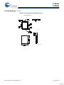
Operational Mode Descriptions
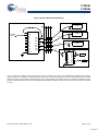
Figure 2 shows the PSCB configured as a zero skew clock buffer. In this mode the 7B991/992 is used as the basis for a low-skew
clock distribution tree. When all of the function select inputs (xF0, xF1) are left open, the outputs are aligned and each drives a
terminated transmission line to an independent load. The FB input is tied to any output in this configuration and the operating frequency
range is selected with the FS pin. The low-skew specification, coupled with the ability to drive terminated transmission lines (with
impedances as low as 50 ohms), enables efficient printed circuit board design.
Figure 3 shows a configuration to equalize skew between metal
traces of different lengths. In addition to low skew between
outputs, the PSCB is programmed to stagger the timing of its
outputs. Each of the four groups of output pairs are programmed
to different output timing. Skew timing is adjusted over a wide
range in small increments with the appropriate strapping of the
function select pins. In this configuration the 4Q0 output is fed
back to FB and configured for zero skew. The other three pairs
of outputs are programmed to yield different skews relative to the
feedback. By advancing the clock signal on the longer traces or
retarding the clock signal on shorter traces, all loads can receive
the clock pulse at the same time.
In this illustration the FB input is connected to an output with 0-ns
skew (xF1, xF0 = MID) selected. The internal PLL synchronizes
Figure 2. Zero Skew and Zero Delay Clock Driver
Figure 3. Programmable Skew Clock Driver
SYSTEM
CLOCK
L1
L2
L3
L4
LENGTH L1 = L2 = L3 = L4
FB
REF
FS
4F0
4F1
3F0
3F1
2F0
2F1
1F0
1F1
4Q0
4Q1
3Q0
3Q1
2Q0
2Q1
1Q0
1Q1
TEST
Z
0
LOAD
LOAD
LOAD
LOAD
REF
Z
0
Z
0
Z
0
LENGTH L1 = L2
L3 < L2 by 6 inches
L4 > L2 by 6 inches
SYSTEM
CLOCK
L1
L2
L3
L4
FB
REF
FS
4F0
4F1
3F0
3F1
2F0
2F1
1F0
1F1
4Q0
4Q1
3Q0
3Q1
2Q0
2Q1
1Q0
1Q1
TEST
Z
0
LOAD
LOAD
LOAD
LOAD
REF
Z
0
Z
0
Z
0
[+] Feedback

CY7B991
CY7B992
Document Number: 38-07138 Rev. *B Page 13 of 19
the FB and REF inputs and aligns their rising edges to ensure
that all outputs have precise phase alignment.
Clock skews are advanced by ±6 time units (tU) when using an
output selected for zero skew as the feedback. A wider range of
delays is possible if the output connected to FB is also skewed.
Since “Zero Skew”, +tU, and –tU are defined relative to output
groups, and since the PLL aligns the rising edges of REF and
FB, you can create wider output skews by proper selection of the
xFn inputs. For example, a +10 tU between REF and 3Qx is
achieved by connecting 1Q0 to FB and setting 1F0 = 1F1 = GND,
3F0 = MID, and 3F1 = High. (Since FB aligns at –4 tU and 3Qx
skews to +6 tU, a total of +10 tU skew is realized.) Many other
configurations are realized by skewing both the outputs used as
the FB input and skewing the other outputs.
Figure 4 shows an example of the invert function of the PSCB.
In this example the 4Q0 output used as the FB input is
programmed for invert (4F0 = 4F1 = HIGH) while the other three
pairs of outputs are programmed for zero skew. When 4F0 and
4F1 are tied high, 4Q0 and 4Q1 become inverted zero phase
outputs. The PLL aligns the rising edge of the FB input with the
rising edge of the REF. This causes the 1Q, 2Q, and 3Q outputs
to become the “inverted” outputs with respect to the REF input.
It is possible to have 2 inverted and 6 non-inverted outputs or 6
inverted and 2 non-inverted outputs by selecting the output
connected to FB. The correct configuration is determined by the
need for more (or fewer) inverted outputs. 1Q, 2Q, and 3Q
outputs can also be skewed to compensate for varying trace
delays independent of inversion on 4Q.
F
Figure 5 shows the PSCB configured as a clock multiplier. The
3Q0 output is programmed to divide by four and is sent to FB.
This causes the PLL to increase its frequency until the 3Q0 and
3Q1 outputs are locked at 20 MHz while the 1Qx and 2Qx
outputs run at 80 MHz. The 4Q0 and 4Q1 outputs are
programmed to divide by two, that results in a 40 MHz waveform
at these outputs. Note that the 20 and 40 MHz clocks fall simul-
taneously and are out of phase on their rising edge. This enables
the designer to use the rising edges of the
1
⁄
2
frequency and
1
⁄
4
frequency outputs without concern for rising edge skew. The
2Q0, 2Q1, 1Q0, and 1Q1 outputs run at 80 MHz and are skewed
by programming their select inputs accordingly. Note that the FS
pin is wired for 80 MHz operation because that is the frequency
of the fastest output.
Figure 6 demonstrates the PSCB in a clock divider application.
2Q0 is fed back to the FB input and programmed for zero skew.
3Qx is programmed to divide by four. 4Qx is programmed to
divide by two. Note that the falling edges of the 4Qx and 3Qx
outputs are aligned. This enables the use of rising edges of the
1
⁄
2
frequency and
1
⁄
4
frequency without concern for skew
mismatch. The 1Qx outputs are programmed to zero skew and
are aligned with the 2Qx outputs. In this example, the FS input
is grounded to configure the device in the 15 MHz to 30 MHz
Figure 4. Inverted Output Connections
FB
REF
FS
4F0
4F1
3F0
3F1
2F0
2F1
1F0
1F1
4Q0
4Q1
3Q0
3Q1
2Q0
2Q1
1Q0
1Q1
TEST
REF
Figure 5. Frequency Multiplier with Skew Connectrions
Figure 6. Frequency Divider Connections
FB
REF
FS
4F0
4F1
3F0
3F1
2F0
2F1
1F0
1F1
4Q0
4Q1
3Q0
3Q1
2Q0
2Q1
1Q0
1Q1
TEST
REF
20 MHz
20 MHz
40 MHz
80 MHz
FB
REF
FS
4F0
4F1
3F0
3F1
2F0
2F1
1F0
1F1
4Q0
4Q1
3Q0
3Q1
2Q0
2Q1
1Q0
1Q1
TEST
REF
20 MHz
5 MHz
10 MHz
20 MHz
[+] Feedback

CY7B991
CY7B992
Document Number: 38-07138 Rev. *B Page 14 of 19
range since the highest frequency output is running at 20 MHz.
Figure 7 shows some of the functions that are selectable on the
3Qx and 4Qx outputs. These include inverted outputs and
outputs that offer divide-by-2 and divide-by-4 timing. An inverted
output enables the system designer to clock different
subsystems on opposite edges, without suffering from the pulse
asymmetry typical of non-ideal loading. This function enables
each of the two subsystems to clock 180 degrees out of phase
and align within the skew specifications.
The divided outputs offer a zero delay divider for portions of the
system that need the clock divided by either two or four, and still
remain within a narrow skew of the “1X” clock. Without this
feature, an external divider is added, and the propagation delay
of the divider adds to the skew between the different clock
signals.
These divided outputs, coupled with the Phase Locked Loop,
enables the PSCB to multiply the clock rate at the REF input by
either two or four. This mode enables the designer to distribute
a low frequency clock between various portions of the system,
and then locally multiply the clock rate to a more suitable
frequency, still maintaining the low skew characteristics of the
clock driver. The PSCB performs all of the functions described in
this section at the same time. It multiplies by two and four or
divides by two (and four) at the same time. In other words, it is
shifting its outputs over a wide range or maintaining zero skew
between selected outputs.
Figure 7. Multi-Function Clock Driver
20 MHz
DISTRIBUTION
CLOCK
80 MHz
INVERTED
Z
0
20 MHz
80 MHz
ZERO SKEW
80 MHz
SKEWED –3.125 ns (–4t
U
)
FB
REF
FS
4F0
4F1
3F0
3F1
2F0
2F1
1F0
1F1
4Q0
4Q1
3Q0
3Q1
2Q0
2Q1
1Q0
1Q1
TEST
REF
LOAD
LOAD
LOAD
LOAD
Z
0
Z
0
Z
0
[+] Feedback

CY7B991
CY7B992
Document Number: 38-07138 Rev. *B Page 15 of 19
Figure 8 shows the CY7B991 and 992 connected in series to construct a zero skew clock distribution tree between boards. Delays
of the downstream clock buffers are programmed to compensate for the wire length (that is, select negative skew equal to the wire
delay) necessary to connect them to the master clock source, approximating a zero delay clock tree. Cascaded clock buffers accumu-
lates low frequency jitter because of the non-ideal filtering characteristics of the PLL filter. Do not connect more than two clock buffers
in series.
Figure 8. Board-to-Board Clock Distribution
SYSTEM
CLOCK
Z
0
L1
L2
L3
L4
FB
REF
FS
4F0
4F1
3F0
3F1
2F0
2F1
1F0
1F1
4Q0
4Q1
3Q0
3Q1
2Q0
2Q1
1Q0
1Q1
TEST
REF
4F0
4F1
3F0
3F1
2F0
2F1
1F0
1F1
4Q0
4Q1
3Q0
3Q1
2Q0
2Q1
1Q0
1Q1
REF
FS
FB
LOAD
LOAD
LOAD
LOAD
LOAD
TEST
Z
0
Z
0
Z
0
[+] Feedback

CY7B991
CY7B992
Document Number: 38-07138 Rev. *B Page 16 of 19
Ordering Information
Accuracy
(ps)
Ordering Code Package Type
Operating
Range
250 CY7B991–2JC 32-Pb Plastic Leaded Chip Carrier Commercial
CY7B991–2JCT 32-Pb Plastic Leaded Chip Carrier - Tape and Reel Commercial
500 CY7B991–5JC 32-Pb Plastic Leaded Chip Carrier Commercial
CY7B991–5JCT 32-Pb Plastic Leaded Chip Carrier - Tape and Reel Commercial
CY7B991–5JI 32-Pb Plastic Leaded Chip Carrier Industrial
CY7B991–5JIT 32-Pb Plastic Leaded Chip Carrier - Tape and Reel Industrial
750 CY7B991–7JC 32-Pb Plastic Leaded Chip Carrier Commercial
CY7B991–7JCT 32-Pb Plastic Leaded Chip Carrier - Tape and Reel Commercial
CY7B991–7JI 32-Pb Plastic Leaded Chip Carrier Industrial
CY7B991–7LMB
[27]
32-Pin Rectangular Leadless Chip Carrier Military
250 CY7B992–2JC 32-Pb Plastic Leaded Chip Carrier Commercial
CY7B992–2JCT 32-Pb Plastic Leaded Chip Carrier - Tape and Reel Commercial
500 CY7B992–5JC 32-Pb Plastic Leaded Chip Carrier Commercial
CY7B992–5JCT 32-Pb Plastic Leaded Chip Carrier - Tape and Reel Commercial
CY7B992–5JI
[27]
32-Pb Plastic Leaded Chip Carrier Industrial
CY7B992–5JIT 32-Pb Plastic Leaded Chip Carrier - Tape and Reel Industrial
750 CY7B992–7JC 32-Pb Plastic Leaded Chip Carrier Commercial
CY7B992–7JCT 32-Pb Plastic Leaded Chip Carrier - Tape and Reel Commercial
CY7B992–7JI 32-Pb Plastic Leaded Chip Carrier Industrial
CY7B992–7LMB
[27]
32-Pin Rectangular Leadless Chip Carrier Military
Pb-Free
250 CY7B991–2JXC 32-Pb Plastic Leaded Chip Carrier Commercial
CY7B991–2JXCT 32-Pb Plastic Leaded Chip Carrier - Tape and Reel Commercial
500 CY7B991–5JXC 32-Pb Plastic Leaded Chip Carrier Commercial
CY7B991–5JXCT 32-Pb Plastic Leaded Chip Carrier - Tape and Reel Commercial
CY7B991–5JXI 32-Pb Plastic Leaded Chip Carrier Industrial
CY7B991–5JXIT 32-Pb Plastic Leaded Chip Carrier - Tape and Reel Industrial
750 CY7B991–7JXC 32-Pb Plastic Leaded Chip Carrier Commercial
CY7B991–7JXCT 32-Pb Plastic Leaded Chip Carrier - Tape and Reel Commercial
500 CY7B992–5JXI 32-Pb Plastic Leaded Chip Carrier Industrial
CY7B992–5JXIT 32-Pb Plastic Leaded Chip Carrier - Tape and Reel Industrial
Note
27.Not recommended for the new design.
[+] Feedback

CY7B991
CY7B992
Document Number: 38-07138 Rev. *B Page 17 of 19
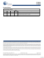
Military Specifications
Group A Subgroup Testing
DC Characteristics
Parameter Subgroups
V
OH
1, 2, 3
V
OL
1, 2, 3
V
IH
1, 2, 3
V
IL
1, 2, 3
V
IHH
1, 2, 3
V
IMM
1, 2, 3
V
ILL
1, 2, 3
I
IH
1, 2, 3
I
IL
1, 2, 3
I
IHH
1, 2, 3
I
IMM
1, 2, 3
I
ILL
1, 2, 3
I
CCQ
1, 2, 3
I
CCN
1, 2, 3
Package Diagrams
Figure 9. 32-Pin Plastic Leaded Chip Carrier
51-85002-*B
[+] Feedback


Document Number: 38-07138 Rev. *B Revised June 22, 2007 Page 19 of 19
PSoC Designer™, Programmable System-on-Chip™, and PSoC Express™ are trademarks and PSoC® is a registered trademark of Cypress Semiconductor Corp. All other trademarks or registered
trademarks referenced herein are property of the respective corporations. Purchase of I
2
C components from Cypress or one of its sublicensed Associated Companies conveys a license under the
Philips I
2
C Patent Rights to use these components in an I
2
C system, provided that the system conforms to the I
2
C Standard Specification as defined by Philips. All products and company names
mentioned in this document may be the trademarks of their respective holders.
CY7B991
CY7B992
© Cypress Semiconductor Corporation, 2001-2007. The information contained herein is subject to change without notice. Cypress Semiconductor Corporation assumes no responsibility for the use of
any circuitry other than circuitry embodied in a Cypress product. Nor does it convey or imply any license under patent or other rights. Cypress products are not warranted nor intended to be used for
medical, life support, life saving, critical control or safety applications, unless pursuant to an express written agreement with Cypress. Furthermore, Cypress does not authorize its products for use as
critical components in life-support systems where a malfunction or failure may reasonably be expected to result in significant injury to the user. The inclusion of Cypress products in life-support systems
application implies that the manufacturer assumes all risk of such use and in doing so indemnifies Cypress against all charges.
Any Source Code (software and/or firmware) is owned by Cypress Semiconductor Corporation (Cypress) and is protected by and subject to worldwide patent protection (United States and foreign),
United States copyright laws and international treaty provisions. Cypress hereby grants to licensee a personal, non-exclusive, non-transferable license to copy, use, modify, create derivative works of,
and compile the Cypress Source Code and derivative works for the sole purpose of creating custom software and or firmware in support of licensee product to be used only in conjunction with a Cypress
integrated circuit as specified in the applicable agreement. Any reproduction, modification, translation, compilation, or representation of this Source Code except as specified above is prohibited without
the express written permission of Cypress.
Disclaimer: CYPRESS MAKES NO WARRANTY OF ANY KIND, EXPRESS OR IMPLIED, WITH REGARD TO THIS MATERIAL, INCLUDING, BUT NOT LIMITED TO, THE IMPLIED WARRANTIES
OF MERCHANTABILITY AND FITNESS FOR A PARTICULAR PURPOSE. Cypress reserves the right to make changes without further notice to the materials described herein. Cypress does not
assume any liability arising out of the application or use of any product or circuit described herein. Cypress does not authorize its products for use as critical components in life-support systems where
a malfunction or failure may reasonably be expected to result in significant injury to the user. The inclusion of Cypress’ product in a life-support systems application implies that the manufacturer
assumes all risk of such use and in doing so indemnifies Cypress against all charges.
Use may be limited by and subject to the applicable Cypress software license agreement.
Document History
Document Title: CY7B991/CY7B992 Programmable Skew Clock Buffer
Document Number: 38-07138
REV. ECN NO. Issue Date
Orig. of
Change
Description of Change
** 110247 12/19/01 SZV Change from Specification number: 38-00513 to 38-07138
*A 1199925 See ECN KVM/AESA Add Pb-free part numbers. Update package names in Ordering Information
table. Remove Pentium reference on page 1.
*B 1286064 See ECN AESA Change status to final
[+] Feedback
-
 1
1
-
 2
2
-
 3
3
-
 4
4
-
 5
5
-
 6
6
-
 7
7
-
 8
8
-
 9
9
-
 10
10
-
 11
11
-
 12
12
-
 13
13
-
 14
14
-
 15
15
-
 16
16
-
 17
17
-
 18
18
-
 19
19


Cypress CY7B992 User manual
- Type
- User manual
- This manual is also suitable for
Ask a question and I''ll find the answer in the document
Finding information in a document is now easier with AI
Related papers

Other documents
-
Sanyo Battery Charger CR17450E-R User manual
-
-
-
-
AG Neovo TSC-30/IC User manual
-
Aeroflex UT200SpW4RTR-EVB User manual
-
Fairchild FSA3357 User manual
-
Infineon BLDC SHIELD_TLE956X User manual
-
Banner ES-TA-3F1 Operating Instructions Manual
-