Texas Instruments Analog Applications Journal Q3, 2002 on-line issue Application Note
- Category
- Musical Instrument Amplifier
- Type
- Application Note

Texas Instruments Incorporated
Analog and Mixed-Signal Products
Analog Applications
Journal
Third Quarter, 2002
© Copyright 2002 Texas Instruments

Texas Instruments Incorporated
2
Analog Applications Journal
Analog and Mixed-Signal Products www.ti.com/sc/analogapps 3Q 2002
IMPORTANT NOTICE
Texas Instruments Incorporated and its subsidiaries (TI) reserve the right to make corrections, modifications,
enhancements, improvements, and other changes to its products and services at any time and to discontinue
any product or service without notice. Customers should obtain the latest relevant information before placing
orders and should verify that such information is current and complete. All products are sold subject to TI’s terms
and conditions of sale supplied at the time of order acknowledgment.
TI warrants performance of its hardware products to the specifications applicable at the time of sale in
accordance with TI’s standard warranty. Testing and other quality control techniques are used to the extent TI
deems necessary to support this warranty. Except where mandated by government requirements, testing of all
parameters of each product is not necessarily performed.
TI assumes no liability for applications assistance or customer product design. Customers are responsible for
their products and applications using TI components. To minimize the risks associated with customer products
and applications, customers should provide adequate design and operating safeguards.
TI does not warrant or represent that any license, either express or implied, is granted under any TI patent right,
copyright, mask work right, or other TI intellectual property right relating to any combination, machine, or process
in which TI products or services are used. Information published by TI regarding third–party products or services
does not constitute a license from TI to use such products or services or a warranty or endorsement thereof.
Use of such information may require a license from a third party under the patents or other intellectual property
of the third party, or a license from TI under the patents or other intellectual property of TI.
Reproduction of information in TI data books or data sheets is permissible only if reproduction is without
alteration and is accompanied by all associated warranties, conditions, limitations, and notices. Reproduction
of this information with alteration is an unfair and deceptive business practice. TI is not responsible or liable for
such altered documentation.
Resale of TI products or services with statements different from or beyond the parameters stated by TI for that
product or service voids all express and any implied warranties for the associated TI product or service and
is an unfair and deceptive business practice. TI is not responsible or liable for any such statements.
Mailing Address:
Texas Instruments
Post Office Box 655303
Dallas, Texas 75265
Copyright © 2002, Texas Instruments Incorporated

Texas Instruments Incorporated
3
Analog Applications Journal
3Q 2002 www.ti.com/sc/analogapps Analog and Mixed-Signal Products
Introduction . . . . . . . . . . . . . . . . . . . . . . . . . . . . . . . . . . . . . . . . . . . . . . . . . . . . . . . . . . . . 4
Data Acquisition
Adjusting the A/D voltage reference to provide gain . . . . . . . . . . . . . . . . . . . . . . . . . . . 5
The purpose of providing gain in an analog-to-digital converter (ADC) is to boost the signal and thereby
improve the signal-to-noise ratio (SNR). This article shows how changing the reference voltage can
achieve gain even in those ADCs that have no PGA.
MSC1210 debugging strategies for high-precision smart sensors . . . . . . . . . . . . . . . . 7
The MSC1210 embeds an 8051 CPU, a 24-bit delta-sigma ADC, and high-performance peripherals to
give a system on-chip solution for high-precision data acquisition systems. This article discusses the
issues involved in smart sensor development, suggests debugging strategies including integrated
development environment simulators, and compares simulators with in-system debuggers.
Using direct data transfer to maximize data acquisition throughput. . . . . . . . . . . . . . 14
Increasing real-time throughput in MCU-based data acquisition systems is a challenge faced in many new
applications. This article offers alternatives that maximize system performance using single-chip mixed-
signal MCU solutions with direct data transfer control.
Amplifiers: Op Amps
Using high-speed op amps for high-performance RF design, Part 2. . . . . . . . . . . . . . 21
Whereas Part 1 focused on how to form an RF stage from op amps and the scattering parameters, this
article focuses on other RF specifications and some of the finer points of RF design.
FilterPro
TM
low-pass design tool. . . . . . . . . . . . . . . . . . . . . . . . . . . . . . . . . . . . . . . . . . . . 24
The FilterPro program aids in the design of low-pass filters implemented with the multiple feedback
(MFB) and Sallen-Key topologies. This article is an introduction to the use and capabilities of FilterPro.
Index of Articles. . . . . . . . . . . . . . . . . . . . . . . . . . . . . . . . . . . . . . . . . . . . . . . . . . . . . . . 29
TI Worldwide Technical Support. . . . . . . . . . . . . . . . . . . . . . . . . . . . . . . . . . . . . . . . 32
Contents
To view past issues of the
Analog Applications Journal
, visit the Web site
www.ti.com/sc/analogapps

Texas Instruments Incorporated
4
Analog Applications Journal
Analog and Mixed-Signal Products www.ti.com/sc/analogapps 3Q 2002
Analog Applications Journal is a collection of analog application articles
designed to give readers a basic understanding of TI products and to provide
simple but practical examples for typical applications. Written not only for
design engineers but also for engineering managers, technicians, system
designers and marketing and sales personnel, the book emphasizes general
application concepts over lengthy mathematical analyses.
These applications are not intended as “how-to” instructions for specific
circuits but as examples of how devices could be used to solve specific design
requirements. Readers will find tutorial information as well as practical
engineering solutions on components from the following categories:
• Data Acquisition
• Amplifiers: Op Amps
Where applicable, readers will also find software routines and program
structures. Finally, Analog Applications Journal includes helpful hints and
rules of thumb to guide readers in preparing for their design.
Introduction
Introduction

5
Analog Applications Journal
Adjusting the A/D voltage reference
to provide gain
The purpose of providing gain in the analog-to-
digital converter (ADC) is to boost the signal and
thereby improve the signal-to-noise ratio (SNR).
Even in ADCs that have internal programmable
gain amplifiers (PGAs), some noise also gets
amplified so that a doubling of the SNR is not
achieved for each doubling of the programmable
gain. This article shows how changing the refer-
ence voltage can achieve gain even in those ADCs
that have no PGA.
The reference voltage defines the range of volt-
age inputs and therefore the size of the LSB. For
an N-bit converter, the LSB is defined as
The full-scale voltage range may not always be
V
REF
; depending on the particular ADC, it could
be 2V
REF
or ±V
REF
. But regardless of how the
output codes are mapped, they are directly influ-
enced by the value of V
REF
. A smaller voltage for
V
REF
will mean that all the output codes are con-
strained to a smaller voltage range and that the
LSB will be a smaller voltage.
The observed noise in the output codes comes
from two sources: (1) analog noise sources (ran-
dom and synchronous) and (2) quantization noise.
When the bit size is large, as in an 8- or 12-bit
ADC, the dominant noise source is expected to be
quantization noise. But for high-resolution convert-
ers of 24 bits, the quantization noise could be the
smallest noise source. Even when quantization noise
is not the major source, reducing it to contribute
even less to the overall result can still be useful.
If we look at the RMS noise as a function of the
reference voltage for the ADS1253 (Figure 1), we
notice that, as a percentage of full-scale, the
smallest noise is achieved with the largest V
REF
.
This is because, as we increase V
REF
, we are
increasing the LSB; therefore, the dominant noise
source starts to be influenced more by quantiza-
tion noise and less by other noise sources. Or at
least, the other noise sources do not increase as
fast and therefore contribute less to the larger
voltage range and larger LSB size.
If we convert the graph in Figure 1 to a graph of
the amplitude of the noise in volts (Figure 2), we
can see that the total noise is actually increasing as
quantization noise becomes a more significant factor.
We can now see that the lowest noise occurs at
a V
REF
of 1 V. This can be a significant factor as we
examine the voltage range of the input signal.
Full-scale voltage
2
N
.
Texas Instruments Incorporated
Data Acquisition
By Russell Anderson (Email: [email protected])
Senior Applications Engineer
3Q 2002 www.ti.com/sc/analogapps Analog and Mixed-Signal Products
30.00
25.00
20.00
15.00
10.00
5.00
0.00
RMS Noise (ppm of Full-scale)
V Voltage (V)
REF
012345
Figure 1. ADS1253 RMS noise vs. V
REF
in ppm of full-scale
9
8
7
6
5
4
3
2
1
0
RMS Noise (µV)
V Voltage (V)
REF
012345
Figure 2. ADS1253 RMS noise vs. V
REF
as µV

Texas Instruments Incorporated
Data Acquisition
6
Analog Applications Journal
Analog and Mixed-Signal Products www.ti.com/sc/analogapps 3Q 2002
Let’s start by looking at the case of a V
REF
of
5 V (Figure 3). If the input signal is smaller than
the full-scale range of 10 V (–5 V to +5 V), then it
would be more useful to plot the noise versus the
signal full-scale value. For example, a noise of 5 ppm
with a 5-V full-scale is 10 ppm if the full-scale
range is only 2.5 V. It is the magnitude of the noise
relative to the signal amplitude that holds our
main interest.
The lowest line in Figure 3 is noise versus V
REF
.
The other lines are noise versus signal voltage.
As can be seen with these different full-scale
signals, the best noise performance is achieved
when the V
REF
matches the full-scale range of the
input signal, although there doesn’t appear to be
any benefit to have a V
REF
lower than 1 V.
With a lower reference voltage, more of the out-
put codes are used with the smaller range of input
voltages. This is the same as providing gain in the
ADC. Normally the reference is 5 V; but with a
V
REF
of 2.5 V the effect is a gain of 2, and a V
REF
of 1.25 V would be equivalent to a gain of 4. A gain
of 5 seems to be the maximum useful gain, with a
V
REF
of 1 V.
Related Web sites
analog.ti.com
www.ti.com/sc/device/ADS1253
RMS Noise (ppm of Full-scale)
V Voltage (V)
REF
012345
40
35
30
25
20
15
10
5
0
0.25-V Signal
0.5-V Signal
1.0-V Signal
2.0-V Signal
Full-scale
Figure 3. RMS noise vs. signal and V
REF
voltage

7
Analog Applications Journal
MSC1210 debugging strategies for
high-precision smart sensors
Introduction
The MSC1210 embeds an 8051 CPU, a 24-bit delta-sigma
ADC, and high-performance peripherals to give a system
on-chip solution for high-precision data acquisition systems
(Figure 1). The MSC1210 therefore provides an excellent
solution for implementing high-precision “smart sensors.”
For high-precision requirements on industrial smart sensor
applications working at a signal range lower than 100 nV,
efficient debugging of code without sacrificing analog per-
formance raises critical issues. This article discusses the
issues involved in smart sensor development, suggests
debugging strategies including integrated development
environment (IDE) simulators, and compares simulators
with in-system debuggers (ISDs).
Smart sensors
Process control instrumentation relies upon high-precision
analog sensor signals for the monitoring of control devices.
The sensor signals are translated to the 4- to 20-mA analog
signal standard, which has long been a standard for indus-
trial process control. With today’s advanced technology,
computers are used to monitor and control a system of
instruments that connect clusters of sensors from a central
point. The sensors are integrated with high-precision
analog-to-digital converters and high-performance proces-
sors to produce smart sensors. Smart sensors replace 4- to
20-mA wiring with a digital network that is more accurate
and more reliable, with simpler interconnections. The
smart sensors also integrate distributed control functions
that improve overall system performance and lower equip-
ment cost.
Texas Instruments Incorporated
Data Acquisition
By Hugo Cheung (Email: [email protected])
Design Engineering Manager, High-Performance Analog, Data Acquisition Products
3Q 2002 www.ti.com/sc/analogapps Analog and Mixed-Signal Products
Clock
Generator
AGND
AV
DD
+AV
DD
V
REF
AGND
REF IN+
REF IN–
DV
DD
DGND
EA
ALE
PSEN
Alternate
Functions
LVD
BOR
POR
WDT
8
8
8
8
ADDR
DATA
ADDR
T2
SPI/EXT
UART2
UART1
EXT
TO
T1
RW
Port0
Port1
ACC
8051
SFR
Port2
Port3
RST
Timers/
Counters
REF OUT
8-bit
PGA Offset
MUX
BUF
PGA
Modulator
Up to 32K
Flash
Digital
Filter
1.2K
SRAM
SPI
FIFO
XIN
XOUT
AINO
AIN1
AIN2
AIN3
AIN4
AIN5
AIN6
AIN7
AINCOM
Figure 1. MSC1210 block diagram

Texas Instruments Incorporated
Data Acquisition
8
Analog Applications Journal
Analog and Mixed-Signal Products www.ti.com/sc/analogapps 3Q 2002
MSC1210 for smart sensors
The MSC1210 (Figure 2) contains many features that are
required by smart sensors, including:
• High-precision ADC: Over 22 effective number of bits
• Embedded sensor signal conditioning circuit: Input buffer,
PGA, offset DAC, gain and offset calibration functions
• Low power consumption to reduce power network
requirements: Under 4 mW
• Enhanced CPU: 4 machine cycles per instruction
8051 core
• Embedded memory: Program (32KB) and data (1.2KB)
• High-performance communication channels: SPI with
deep FIFO, dual UARTs
• Robust industrial environment circuits: Low-voltage
detect, brownout detect, watchdog timer, wide operating
conditions (power supply 2.7 to 5.25 V and operating
temperature –40 to +85°C)
Smart sensors code development
Since a smart sensor is an integrated
system with complicated sensor signal
conversion, process control, and net-
working, the code development for
smart sensors has to resolve problems
such as the following:
• Development system effects on the
analog signal precision
• Physical size of the target hardware
• Development host-to-target-system
communication media
• Real-time control and networking
timing
• Development system power source
The microsystem controller (MSC)
provides various debugging strategies
that meet the tough development
requirements. Figure 3 depicts the
available debugging strategies for MSC
devices. The strategies range from
simulation-based to in-system debug-
ging. In-system debuggers (ISDs) are
further divided into software-based and
hardware-based. Among the available
strategies, the Keil and Raisonance sim-
ulators, the MSCMon terminal monitor,
and the Keil ISD51 IDE monitor are suit-
able for smart sensor code development.
IDE simulator for initial smart
sensor coding
The integrated development environment
(IDE) is a set of development tools
integrated in a user-friendly GUI suite.
Development tools integrated into the
same environment shorten the code
development cycle and reduce code
errors, which also enhances code quality.
IDEs provide tools such as editors,
assemblers, compilers, linkers, project
management, and revision control, as well
Digital Network
Smart Sensor Nodes
PC
A
c
t
u
a
t
o
r
S
e
n
s
o
r
Processor
Figure 2. Smart sensor system
Terminal Monitor: IDE Monitor:
MON51
MSCMON**
Keil Mon 51
Keil ISD51**
Raisonance
Mon51
Simulators:
Keil Simulator**
Raisonance Simulator**
In-circuit Emulator: Built-in Debug
Module*
*Not available
**Recommended for smart sensor development
Software ISDs
Hardware ISDs
In-System Debuggers (ISDs)
MSC Debugging
Strategies
HiTex
MX51
Figure 3. MSC debugging strategies tree
Simulated MSC Modules
Single-step
Break
Code Performance
Code Coverage
Memory View/Edit
Disassembly
GUI
24-bit ADC
On-chip Memories
8051 CPU
Dual UART
T0/1/2
SPI
Other Peripherals
MSC Device
User ASM
User C
PC Comm Port
PC Simulator
Figure 4. IDE simulator conceptual block diagram

Texas Instruments Incorporated
Data Acquisition
9
Analog Applications Journal
3Q 2002 www.ti.com/sc/analogapps Analog and Mixed-Signal Products
as device simulators in the same
environment. Commonly avail-
able simulators of IDEs simulate
8051 devices within Microsoft
®
Windows
®
. UNIX platform sim-
ulators are not as common as
the Windows version.
Simulators enable users to
simulate code execution with-
out actual target hardware.
Users can verify algorithms
and timing, and simulate
peripherals, interrupts, and
I/O. This is important because
it allows the user to start code
development and evaluate sys-
tem performance even before
the target hardware is available.
Figure 4 depicts the conceptual
block diagram of the IDE simu-
lator for the MSC device. Users
can perform disassembly, break
point, memory watch/modify,
code execution trace, and
peripheral monitoring.
Simulators also support code
coverage tools that “mark” the
code that has been executed.
Simulators also provide
performance analyzer tools
that record the execution time
for functions so that the user
can profile code performance.
However, the most common
simulator operation is code
stepping. Simulators support
single-step with “step-into” a
target function or “step-over”
the function. The machine
cycle count is accurate in the
simulators; thus execution
time can be easily evaluated
for inefficiencies.
Common PC Windows IDE
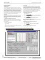
simulators include the Keil
debugger (Figure 5) and the
Raisonance debugger
(Figure 6). The Keil IDE user’s
manual is a good reference for
the detailed simulator opera-
tions. The Raisonance IDE has
debugging features similar to
the Keil IDE. See “Related Web
sites” at the end of this article.
Figure 5. Keil IDE simulator
Figure 6. Raisonance IDE simulator

Texas Instruments Incorporated
Data Acquisition
10
Analog Applications Journal
Analog and Mixed-Signal Products www.ti.com/sc/analogapps 3Q 2002
Advantages of using IDE simulators for smart
sensor code developments
• Code simulation is a low-cost approach to code develop-
ment, since no development hardware tools are required.
• Code development can be started before target system
hardware is available.
• IDE simulators are best suited for initial smart sensor
code development.
Disadvantages of using IDE simulators for smart
sensor code development
• A precision analog signal cannot be simulated.
• Network timing and real-time interactions in process
control are difficult to simulate.
• When code development reaches the stage that requires
target hardware, debugging in the target system or ISD
is needed.
Ad hoc debugging style is insufficient for smart
sensor development
Instead of PC simulation, the ISD executes and debugs code
in the actual target system. Ad hoc debugging—simply
inserting the debug code wherever it is needed—is the
easiest method. For example, simply add a printf state-
ment and inspect the result. This style is good for simple
code testing. However, when the code size increases, the
number of printf statements will become unmanageable.
Smart sensor in-system debuggers
The ISD development environment embeds debugging
support within the smart sensor (Figure 7). The develop-
ing code will process real system input from the sensors
and provide instantaneous system response instead of
system simulation. Therefore, system-level issues such as
sensor accuracy, control system stability, or sensor network
throughput can be resolved. As shown in Figure 3, there
are two categories of ISDs—software-based and hardware-
based. Software-based ISDs are further divided into
terminal-based and IDE-based. Terminal-based debugging
includes a general-purpose monitor and an on-chip debug-
ger. IDE-based debugging includes a source-level monitor
and Flash-enabled ISD. Hardware-based ISDs are further
divided into an in-circuit emulator (ICE) and a built-in
debugger module (BDM).
Since smart sensors are compact systems, most of them
cannot accommodate external memory devices that occupy
extra board space, increase power consumption, and
increase system cost. Therefore, the resources to provide
an ISD setup must be included within the MSC1210.
Those resources include ISD code space, a CPU time-to-
processing ISD routine, and an ISD port.
Software ISDs that require external memory (Figure 3),
such as the general-purpose MON51, Keil MON51, and
Raisonance MON51, are not the best candidates for smart
sensor development. Neither are hardware ISDs that
require an extra ICE connection bus, consume more ICE
bus power, and have higher system noise created by the
ICE bus. ICEs are not recommended for in-system debug-
ging. The ICE and ISD with external memory should be
used only as an intermediate development setup.
Software ISD debugging style is ideal for smart
sensor development
The embedded monitor for remote target systems such as
smart sensors is an ISD software monitor that resides in
code memory. The ISD monitor program (Figure 8) acts
as an interpreter between the user code and the debug
terminal program. The monitor allows code to be down-
loaded into the target system memory from the debug
terminal (such as PC terminal programs using the on-chip
UART) and then allows debugging functions—such as
memory or SFR read/modify, CPU status request, user
routine calls, single-step, or break—to be performed.
Digital Network
Smart Sensor Nodes
Optional
Debug Port
PC
Network Protocol
Processor
Sensor &
Actuator
ISD
F/W &
H/W
Debug
Terminal
Figure 7. Smart sensor ISD configuration
Load
Single-step
SFR R/W
Memory R/W
CPU Status
24-bit ADC
On-chip Memories
8051 CPU
Dual UART
T0/1/2
SPI
Other Peripherals
MSC Device
Remote MSC Smart Sensor
Sensor
Network
Optional
Debug
Port
Embedded ISD
Monitor Code @
Flash Memory
Sensor &
Actuator
Figure 8. ISD monitor conceptual block diagram

Texas Instruments Incorporated
Data Acquisition
11
Analog Applications Journal
3Q 2002 www.ti.com/sc/analogapps Analog and Mixed-Signal Products
Sensor network as debug port
The debug port connection to the debug terminal creates
a wiring problem for the compact remote smart sensor.
An alternative is to communicate debug commands and
responses and even to load user code between the sensor
and terminal via the sensor network. However, there are
so many sensor network standards being used that a cus-
tom ISD monitor code including sensor network process-
ing is needed.
Downloading user code through sensor network
or debug port
Programming microcontroller-embedded Flash memory
with serial/parallel Flash programming operations is a
function commonly available for many microcontrollers,
including MSC1210. User code may be downloaded to
remote sensors through debug port UART0 by putting the
MSC1210 remote sensor in Flash programming mode.
When a debug port is not feasible, or the number of sensor
network connections must be minimized, user code may
be downloaded during normal user operation via the sen-
sor network. The MSC1210 has a program Flash memory
self-update capability. In other words, when executing the
embedded ISD monitor Load User Code command, the
monitor program that resides in the MSC1210’s embedded
Flash memory will download the user code and store it in
the same Flash memory.
MSC1210 IAP Flash memory
While the user code is being downloaded, the embedded
Flash memory is busy performing write or erase operations,
during which CPU execution from the Flash memory is
not possible. The MSC1210 has an embedded 2KB boot-
loader ROM that provides Flash write/erase routines. The
ROM routines are used for in-application programming
(IAP) of the embedded Flash memory. The MSC1210 user
application code, such as the ISD monitor program, calls
the ROM routines to program the Flash memory.
ISD monitor—embedded MSCMon
The ISD monitor may be modified with general-purpose
monitor programs that are available free from the Internet.
Many of them are tested for MSC1210, such as MonPlus by
Steve Kemplin, PaulMon by Paul Stoffregen, and Ultramon
by an unknown author.
MSCMon—an on-chip MSC monitor program
Besides the Flash IAP routines, the embedded ROM also
includes other supporting routines (see Code Listing 1)
for the monitor program or applications. Using the
boot-loader debug subroutines, such as autobaud,
Code Listing 1: BootROM subroutine prototypes
void put_string(char code *string); // print a string to SBUF0
//erase a program or data memory page
char page_erase (int faddr, char fdata, char fdm);
//write a program or data memory byte, sel program/data with MXWS bit
char write_flash (int faddr, char fdata);
// write a program or data memory byte with 3 retries
char write_flash_chk (int faddr, char fdata, char fdm)
// Write A to @DPTR, select program/data with MXWS bit
// ASM write_flash_byte ;
char faddr_data_read(char); // read a HW config memory byte
char data_x_c_read(int addr, char fdm); // read a xdata or code byte
void tx_byte(char c); //transmit c to SBUF0
void tx_hex(char); // transmit hex of c to SBUF0
void putok(void); // transmit “ok” to SBUF0
char rx_byte(void); // receive a byte from SBUF0
char rx_byte_echo(void); // receive and echo a byte from SBUF0
char rx_hex_echo(void); // receive two hex digits from SBUF0
// receive and echo four hex digits from SBUF0, return R6:R7 as int type
int rx_hex_word_echo(void);
// receive four hex digits from SBUF0, return R6:R7 as int type
int rx_word_echo(void);
// receive and echo four hex digits from SBUF0, return R7:R6 as stack order
int rx_hex_word_echo(void);
void autobaud(void); // SBUF0 auto baud rate setup with T2
void putspace4(void); // print 4,3,2,1 ASCII Space, Carriage Return
void putspace3(void);
void putspace2(void)
void putspace1(void)
void putcr(void);
// ASM cmd_parser ; Command parser entry point
// ASM monitor_isr ; Monitor ISR entry point

Texas Instruments Incorporated
Data Acquisition
12
Analog Applications Journal
Analog and Mixed-Signal Products www.ti.com/sc/analogapps 3Q 2002
put_string, or cmd_parser, gives
the user the lowest-overhead debug-
ging setup—MSCMon (see Code
Listing 2).
The MSC-embedded debug sub-
routines support not only the basic
debugging commands such as
S-SingleStep, B-Break, and
Q-Continue; they also support
Flash memory commands such as
CP-CodePageErase, CW-CodeWrite,
XP-XDataPageErase, and
L-LoadFlash. The MSCMon trans-
lates into very low debug overhead;
the minimum-configuration MSCMon
needs only 29 bytes of Flash code
space. In addition, since user code is
stored in Flash memory, the down-
loaded code can be used for the final
application. The complete command listing is shown in
Figure 6. Typically, the MSC monitor is resident in Flash
memory, and the Load User Code command is used to
download user code. Since the memory requirement for
the MSC monitor is very low, the user code may be linked
with the MSCMon.
The MSCMon requires a PC debug terminal such as
Hyper-term, Tera-term, Procomm, or Telix. A user sensor
network program is needed when a debug port and debug
terminal are not available.
Assembly-level and source-level debugging
Typical debug terminal programs using RS-232 ports have
no information about the source code or monitor operation.
Code Listing 2: Minimum-configuration MSC monitor—MSCMon
$include (reg1210.inc)
CSEG at 807FH
; HCR0: PML=0 RSL=1 to protect 0~1000H
db 0BFH Flash
CSEG at 0000H ; Monitor code start
LCALL autobaud
mov R6, #high greet
mov R7, #low greet
lcall _put_string
LJMP cmd_parser
greet: db 0ah,0dh,”MSC Monitor”,0
CSEG at 033H
; any other AuxInt handler
LJMP monitor_isr
Figure 9. Keil ISD51 source-level debugging
Source-level debugging functions such as single-step
require a symbol table and machine-code-to-source-code
relationship. Therefore, only assembly-level debugging is
supported. However, PC IDE programs have special hand-
shaking with monitor programs for extra source code
information that a general-purpose monitor or MSCMon
does not have. These sophisticated source-level interfaces,
when combined with the debugging commands, provide a
user-friendly environment.
The Keil ISD51 monitor is a Flash memory resident
program that communicates with the IDE to achieve source-
level debugging. The IDE GUI greatly enhances the
debugging efficiency (Figure 9). At any time, the user can
monitor the CPU register and any memory contents. Since

Texas Instruments Incorporated
Data Acquisition
13
Analog Applications Journal
3Q 2002 www.ti.com/sc/analogapps Analog and Mixed-Signal Products
it is source-level, the debugging quality is much better than
with assembly-level monitors. Because of the small size
requirement for the ISD51, it is compiled and downloaded
together with user code in the target system. The MSC1210
has a built-in hardware break point that detects the break
address with hardware. The ISD51 fully utilizes the hard-
ware break-point function, improving the execution per-
formance over that of the software by a hundredfold.
Although the Keil ISD51 is a very attractive tool, an
RS-232 debug port is needed. Again, the setup for the ISD
monitor to communicate with the custom sensor network
has to be independently developed.
Conclusion
Since the ISD monitor tools reside in the smart sensor, the
target smart sensor does not compromise analog perform-
ance from the code-development setup. The MSCMon and
Keil ISD51 monitors have low code-space overhead. If
code space is sensitive in some applications, a larger-
memory version of the MSC1210 family of devices can be
used during prototyping, then switched to a lower-memory
option for the production unit. The ISD monitors do not
need extra hardware for debugging, which implies low
development cost.
References
For more information related to this article, you can down-
load an Acrobat Reader file at www-s.ti.com/sc/techlit/
litnumber and replace “litnumber” with the TI Lit. # for
the materials listed below.
Document Title TI Lit. #
1. “Precision Analog-to-Digital Converter
(ADC) with 8051 Microcontroller and
Flash Memory,” MSC1210 Data Sheet . . . . . . . .sbas203
2. “ISD51 In-System Debugger,”
www.keil.com/c51/isd51.htm —
3. “Installing and Using the Keil Monitor-51,”
Application Note 152, www.keil.com/appnotes/
files/apnt_152.pdf —
4. Russell Anderson, “Programming the
MSC1210,” Application Report . . . . . . . . . . . . .sbaa076
5. “MSC1210 Precision ADC with 8051
Microcontroller and Flash Memory
Evaluation Module,” User’s Guide . . . . . . . . . . .sbau073
6. “MX51, AX51,” www.hitex.com/
products.html?axmx51.html~content —
7. Russell Anderson, “Debugging Using the
MSC1210 Boot ROM Routines,”
Application Report . . . . . . . . . . . . . . . . . . . . . . .sbaa079
Related Web sites
analog.ti.com
www.ti.com/sc/device/MSC1210
www.hitex.com
www.keil.com/demo/
www.raisonance.com/download/index.php

14
Analog Applications Journal
Analog and Mixed-Signal Products www.ti.com/sc/analogapps 3Q 2002
Using direct data transfer to maximize
data acquisition throughput
Introduction
Increasing real-time throughput in MCU-based data acqui-
sition systems is a challenge faced in many new applications.
By definition, real-time applications must sample, digitize,
transfer, and process acquired data before subsequent
samples are made. Adequate CPU reserves must also be
kept between samples to allow digital signal processing of
the data. When acquisition rates exceeds 10 kSPS, engi-
neers are often forced to make compromises due to the
extreme overhead placed on the MCU. The basic task of
moving acquired data becomes dominant and often
unmanageable. Increasing CPU clock speeds or using
specialized digital signal processors (DSPs) is often the
only solution to meeting high data acquisition rates. This
article offers alternatives that maximize system perform-
ance using single-chip mixed-signal MCU solutions with
direct data transfer control.
System example using an external ADC
A typical multi-chip MCU-based data acquisition system is
presented in Figure 1. The system includes an MSP430F123
MCU and a TLV1549 10-bit ADC. A low-power, 32-kHz
watch crystal is used for the auxiliary clock (ACLK); and
the MCU’s internal digitally controlled oscillator (DCO) at
its default frequency of ~1 MHz is used for the CPU’s
master clock (MCLK). The system samples a sensor signal
with 10 bits of accuracy and transfers the acquired output
code to on-chip RAM at 8192 samples per second. After 20
ADC samples have been acquired, the MCU will process
the data stored in RAM. An application with such require-
ments could be a DTMF detection system.
The interface between the ADC and the MCU is glue-
less, using the MCU’s integrated USART in SPI mode. To
support the 8192-sample rate, the MCU’s 16-bit Timer_A
uses the ACLK with capture compare register 0 (CCR0)
configured to trigger an interrupt service routine
(CCR0_ISR) at the required sampling rate.
Inside the Mainloop, the MCU is normally in low-power
mode 3 (LPM3). CCRO_ISR wakes the CPU, and an ADC
sample is made. For each CCR0_ISR, software enables the
ADC by resetting the ADC conversion start CS. Data are
exchanged between the ADC and MCU as two 8-bit bytes
for each 10-bit conversion. The software starts and times a
conversion by writing two dummy bytes back-to-back to
the MCU’s USART transmit buffer (TXBUF). The software
then polls the USART receive interrupt flag (RXIFG) to
indicate the receipt of a data byte from the ADC to the
USART’s receive buffer (RXBUF). Two bytes are received,
packed, and transferred to MCU RAM with software and a
pointer register R4. CS is reset, disabling the ADC. After
20 samples have been acquired, the Mainloop breaks
from LPM3; and the data are processed as shown in Code
Listing 1.
For each external ADC measurement, 16 I/O clocks are
required. The MCU’s USART transfers data at half of the
applied clock—the DCO, the same clock source used for
the CPU MCLK. Thus 16 I/O clocks are equivalent to
32 MCLKs. The CCR0_ISR overhead and transfer of the
ADC conversion code to memory takes additional cycles,
for a total of 83 CPU MCLKs for each sample. With 8192
samples per second, an external ADC, and a 1-MHz MCLK,
the CPU overhead is calculated as follows:
The CPU is loaded 68%, as shown in Figure 2. The
Timer_A CCR0_ISR and two CPU registers are also required.
CPU
overhead (external ADC)
=
×
=
83 8192
1000000
068.
Texas Instruments Incorporated
Data Acquisition
By Mark Buccini (Email: [email protected])
MSP430 Applications Manager
TLV1549
32 kHz
MSP430F123
V
REF+
Analog
REF–
CC
V
/NMI
P3.0
P3.2/SOMI
P3.3/UCLK
V
CC
SS
RST
CS
DOUT
IOCLK
GND
Figure 1. External ADC MCU data
acquisition system
122 244 366
Processor Activity (%)
Activity Per Sample (µs)
100
Figure 2. External ADC with MCU data
acquisition system activity

Texas Instruments Incorporated
Data Acquisition
15
Analog Applications Journal
3Q 2002 www.ti.com/sc/analogapps Analog and Mixed-Signal Products
Code Listing 1: MSP430F123/TLV1549 software example
#include “msp430x12x.h”
;******************************************************************************
; MSP-FET430P120 Demo - USART0 SPI Interface to TLV1549 10-bit ADC
;
; M.Buccini - Texas Instruments, Inc - July 2002
;******************************************************************************
;——————————————————————————————————————————————————————————————————————————————
ORG 0F000h ; Program Reset
;——————————————————————————————————————————————————————————————————————————————
RESET mov.w #0300h,SP ; Initialize stackpointer
StopWDT mov.w #WDTPW+WDTHOLD,&WDTCTL ; Stop watchdog timer
SetupP3 bis.b #0Ch,&P3SEL ; P3.2,3 SPI option select
bis.b #09h,&P3DIR ; P3.3,0 output direction
SetupSPI bis.b #USPIE0,&ME2 ; Enable USART0 SPI
bis.b #CKPH+SSEL1+SSEL0+STC,&UTCTL0 ; SMCLK, 3-pin
bis.b #CHAR+SYNC+MM,&UCTL0 ; 8-bit SPI Master
mov.b #02h,&UBR00 ; SMCLK/2 for baud rate
clr.b &UBR10 ; SMCLK/2 for baud rate
clr.b &UMCTL0 ; Clear modulation
bic.b #SWRST,&UCTL0 ; **SWRST**
SetupTA mov.w #TASSEL0+TACLR,&TACTL ; ACLK, clear TAR
SetupC0 mov.w #CCIE,&CCTL0 ; CCR0 interrupt enabled
mov.w #4-1,&CCR0 ; CCR0 counts to 4
bis.w #MC0,&TACTL ; Start Timer_a in upmode
eint ; Enable interrupts
;
Mainloop clr.w R4 ; Clear pointer
Meas1549 bis.w #LPM3,SR ;
bic.b #01h,&P3OUT ; Enable TLV1549, /CS reset
mov.b #00h,&TXBUF0 ; Dummy write to start SPI
mov.b #00h,&TXBUF0 ;
L1 bit.b #URXIFG0,&IFG2 ; RXBUF ready?
jnc L1 ; 1 = ready
mov.b &RXBUF0,R5 ; R5 = 00|MSB
swpb R5 ; R5 = MSB|00
L2 bit.b #URXIFG0,&IFG2 ; RXBUF ready?
jnc L2 ; 1 = ready
mov.b &RXBUF0,R6 ; R6 = 00|LSB
add.w R6,R5 ; R6 = MSB|LSB
bis.b #01h,&P3OUT ; Disable TLV1549, /CS set
mov.w R5,0200h(R4) ;
incd.w R4 ;
cmp.w #040,R4 ; R4 = 20 words?
jne Meas1549 ;
; ** SIGNAL PROCESSING HERE
jmp Mainloop ; Again
;
TA0_ISR mov.w #GIE ,0(SP) ; System active on reti
reti ;
;
ORG 0FFFEh ; MSP430 RESET Vector
DW RESET ;
ORG 0FFF2h ; Timer_A0 Vector
DW TA0_ISR ;
END

Texas Instruments Incorporated
Data Acquisition
16
Analog Applications Journal
Analog and Mixed-Signal Products www.ti.com/sc/analogapps 3Q 2002
Using an internal ADC
To miniaturize applications and reduce system cost, an
ADC is commonly integrated into an MCU. This integration
provides a more compact system on-chip solution with the
twofold benefit of reduced board space and the elimination
of a serial port required for communicating between the
MCU and ADC. An example of an MCU with an integrated
10-bit ADC is the MSP430F1232, as shown in Figure 3.
The MSP430F1232 eliminates the external 10-bit ADC,
using the integrated ADC10 instead. CCR0_ISR is again
used to wake the CPU from LPM3 in the Mainloop, as
shown in Code Listing 2. The Mainloop manages the
acquisition of 20 samples, storing the output code from
the ADC10 memory buffer (ADC10MEM) to RAM. Only
40 MCLKs are required for each sample. With the internal
ADC10 and a 1-MHz MCLK, the CPU overhead to support
the 8192-sample rate is calculated as follows:
CPU
overhead (internal ADC)
=
×
=
40 8192
1000000
033.
Code Listing 2: MSP430F1232 ADC10 software example
#include “msp430x12x2.h”
;******************************************************************************
; MSP-FET430P120 Demo - ADC10 Sample A0 20x, AVcc, TA0 ISR
;
; M.Buccini - Texas Instruments, Inc - July 2002
;******************************************************************************
;——————————————————————————————————————————————————————————————————————————————
ORG 0F000h ; Program Reset
;——————————————————————————————————————————————————————————————————————————————
RESET mov.w #0300h,SP ; Initialize stackpointer
StopWDT mov.w #WDTPW+WDTHOLD,&WDTCTL ; Stop watchdog timer
SetupADC10 mov.w #ADC10SHT_2+ADC10ON,&ADC10CTL0 ; 16x
bis.b #01h,&ADC10AE ; P2.0 ADC10 option select
SetupTA mov.w #TASSEL0+TACLR,&TACTL ; ACLK, clear TAR
SetupC0 mov.w #CCIE,&CCTL0 ; CCR0 interrupt enabled
mov.w #4-1,&CCR0 ; CCR0 counts to 4
bis.w #MC0,&TACTL ; Start Timer_a in upmode
eint ; Enable interrupts
;
Mainloop clr.w R4 ; Clear pointer
MeasADC10 bis.w #ENC+ADC10SC,&ADC10CTL0 ; Start sampling/conversion
bis.w #LPM3,SR ;
mov.w &ADC10MEM,0200h(R4) ;
incd.w R4 ;
cmp.w #040,R4 ; R4 = 20 words?
jne MeasADC10 ;
; ** SIGNAL PROCESSING HERE
jmp Mainloop ; Again
;
TA0_ISR mov.w #GIE ,0(SP) ; System active on reti
reti ;
;
ORG 0FFFEh ; MSP430 RESET Vector
DW RESET ;
ORG 0FFF2h ; Timer_A0 Vector
DW TA0_ISR ;
END
32 kHz
MSP430F1232
V
/NMI
A0
V
CC
SS
RST
Figure 3. MSP430F1232 MCU data
acquisition system

Texas Instruments Incorporated
Data Acquisition
17
Analog Applications Journal
3Q 2002 www.ti.com/sc/analogapps Analog and Mixed-Signal Products
The CPU is loaded 33%, as shown in Figure 4. Using an
internal ADC reduces the CPU overhead by 50% compared
to when an external ADC is used. The CPU overhead
reduction is accomplished by eliminating the software and
delay associated with servicing the serial port communica-
tion between the MCU and the external ADC. The free
serial port can be used for other features or completely
eliminated in cost-sensitive applications.
Data transfer controller
In addition to ADC10, the MSP430F1232 contains a data
transfer controller (DTC). The DTC provides the capability
of automatically transferring conversion code from the
ADC10 output buffer memory (ADC10MEM) directly to
on-chip memory—without CPU intervention, as shown in
Figure 5. The start address (ADC10SA) of the transfer
sequence can point anywhere in the MCU’s memory. The
total number of conversions is configured with the
ADC10DTC1 control register. The DTC can transfer ADC10
output code in a single-block sequence or a dual-block
sequence, both with or without repeating, and both with
or without interrupt capability. In the example, the DTC
transfers code into a single block, repeating with interrupt.
The DTC does not require the CPU to transfer
ADC10MEM to memory, but it does require one memory
data bus (MDB) clock, which is the same as the MCLK
used by the CPU. When an MDB clock is required for
122 244 366
Processor Activity (%)
Activity Per Sample (µs)
100
Figure 4. MSP430F1232 ADC10 data
acquisition system activity
AV
CC
AV
SS
Sample
&
Hold
ADC10SC
Oscillator
Sampling/
Conversion
Control
V
eREF+
VV
eREF– REF–
/
V
REF+
V
R–
10-bit SAR
1.5-V or 2.5-V
Reference
ADC10MEM
Conversion
Clock
V
R–
AV
CC
Multiplexer
A0
A1
A2
A3
A4
A5
A6
A7
RAM, Flash...
ADC10SA
ADC10SA+n
TA1
TA0
TA2
ACLK
MCLK
SMCLK
Data Transfer
Controller
Figure 5. MSP430F1232 ADC10 block diagram
transfer, the DTC will halt any CPU activity for exactly one
clock. This halt is to prevent memory conflict between the
DTC and CPU. In effect, the DTC “steals” one MCLK from

Texas Instruments Incorporated
Data Acquisition
18
Analog Applications Journal
Analog and Mixed-Signal Products www.ti.com/sc/analogapps 3Q 2002
the CPU for each DTC transfer. This may be interpreted
as CPU overhead. If the CPU is not active and using the
MDB, the effect of the DTC is of no consequence.
With 8192 samples per second, a 1-MHz CPU MCLK, and
use of the DTC, the CPU overhead is calculated as follows:
The CPU is loaded less than 1% while sustaining an
8192-sample rate, as shown in Figure 6. The DTC allows
over 99% of the CPU resources to be available for digital
signal processing and control. In the example, the DTC
will set the ADC10 interrupt after a block of 20 samples
has been transferred. The function of R4, used as a loop
counter in the previous two examples, is no longer required.
The DTC and ADC10 interrupt service routine (ADC10_ISR)
will wake the CPU from LPM3 in Mainloop only after a
complete block of 20 samples has been taken and trans-
ferred automatically to RAM, as shown in Code Listing 3.
CPU
overhead (internal ADC with DTC)
=
×
=
1 8192
1000000
0 008.
Code Listing 3: MSP430F1232 ADC10 with DTC software example
#include “msp430x12x2.h”
;******************************************************************************
; MSP-FET430P120 Demo - ADC10 Sample A0 20x, AVcc, TA0 Trigger, DTC DCO
;
; M.Buccini - Texas Instruments, Inc - July 2002
;******************************************************************************
;——————————————————————————————————————————————————————————————————————————————
ORG 0E000h ; Program Start
;——————————————————————————————————————————————————————————————————————————————
RESET mov.w #0300h,SP ; Initialize stackpointer
StopWDT mov.w #WDTPW+WDTHOLD,&WDTCTL ; Stop WDT
SetupADC10 mov.w #SHS_2+CONSEQ_2,&ADC10CTL1 ; TA0 trigger
mov.w #ADC10SHT_2+ADC10ON+ADC10IE,&ADC10CTL0;
mov.b #ADC10CT,&ADC10DTC0 ; Continuos
mov.b #020,&ADC10DTC1 ; 20 conversions
bis.b #001h,&ADC10AE ; P2.0 ADC10 option select
SetupTA mov.w #TASSEL0+TACLR,&TACTL ; ACLK, clear TAR
SetupC0 mov.w #OUTMOD_4,&CCTL0 ; CCR0 toggle
mov.w #2-1,&CCR0 ; PWM Period
mov.w #0200h,&ADC10SA ; Data buffer start
bis.w #ENC,&ADC10CTL0 ; Sampling and conversion ready
bis.w #MC0,&TACTL ; Start Timer_a in upmode
eint ; Enable interrupts
;
Mainloop bis.w #LPM3,SR ; LPM3, ADC10 ISR will force exit
; ** SIGNAL PROCESSING HERE
jmp Mainloop ; Again
;
ADC10_ISR mov.w #GIE,0(SP) ; System active on reti
reti ;
;
ORG 0FFFEh ; MSP430 RESET Vector
DW RESET ;
ORG 0FFEAh ; ADC10 Vector
DW ADC10_ISR ;
END
122 244 366
Processor Activity (%)
Activity Per Sample (µs)
100
Figure 6. MSP430F1232 ADC10 with DTC data
acquisition system activity

Texas Instruments Incorporated
Data Acquisition
19
Analog Applications Journal
3Q 2002 www.ti.com/sc/analogapps Analog and Mixed-Signal Products
DTC channel scanning
Some systems, such as an electricity meter, require channel
scanning, mixing alternate samples of voltage and current.
Using software and an internal or external ADC to switch
channels adds at least 10 MCLK cycles of overhead for
each sample. At an 8192-sample rate with a 1-MHz MCLK,
software-based channel scanning adds an additional 0.08%
CPU overhead. DTC provides the ability to scan a mix of
different channels (i.e., A2, A1, A0, A2, A1, A0...) automati-
cally without any CPU resources. If channel scanning is
useful in an application, the benefits of using a DTC are
magnified.
SOC-introduced phase error
High-performance data acquisition systems must take into
account several factors in addition to the sampling speed
discussed so far. In many applications, an analog sensor
output must be sampled at very exact intervals to detect
small phase changes. For example, stimuli may be presented
to sensor input, with a delayed response measured at an
output. For demonstration purposes, a repeating 10-kHz
triangle signal from 0 to 3 V is shown in Figure 7. The rate
of change of the triangle signal is calculated as follows:
Signal(dv/dt) = 3 V/100 µs = 30 mV/µs
With a 10-bit ADC in a 3-V system, the ADC step size is the
ADC reference (assumed to be the supply) divided by 1024.
ADC10(step) = 3 V/1024 = 3 mV
If only software is used to trigger an ADC start of
conversion (SOC), some uncertainty or jitter will always
be present. Other always-present CPU activity such as
servicing an interrupt or UART handler causes this
uncertainty. Unless all other CPU activity is ceased prior
to a software-initiated SOC—very impractical for modern
embedded applications—some uncertainty with software-
triggered SOC will always be possible.
For example, using the example system with an MCLK
of 1 MHz (1-µs clock), the effect of just one clock of SOC
uncertainty will introduce 30 mV of ADC uncertainty or
jitter error. This 30 mV of uncertainty error is equivalent
to 10 10-bit steps. The 10-bit ADC output code with 1 µs
of SOC jitter is reduced to an accuracy of a 7-bit ADC!
When an ADC10 is used, a CCRx output can automati-
cally trigger ADC10 SOC with the precision of the used
1-µs SOC Jitter
30-mV Error
Target ADC SOC
100 µs
3 V
Figure 7. ADC sampling uncertainty error
timer clock—all interrupt and latency uncertainty associ-
ated with software-driven SOC is removed completely
from the system. The ADC10 SOC will be triggered with
perfect timing, using the CCRx hardware asynchronously
and regardless of other CPU, software, or system activity.
DTC system throughput performance increase
Using DTC in data acquisition applications relieves the CPU
from the burden of transferring ADC output code to mem-
ory. The DTC in itself reduces CPU loading by a factor of 40×
compared with using an internal ADC10, and by a factor of
greater than 80× compared with using an external ADC.
In the example using an external ADC, the MCU MCLK
would need to be increased to 4 MHz to acquire the ADC’s
maximum conversion rate of 38 kSPS—and the CPU
would be loaded 79%. At the same 4-MHz MCLK and with
the MSP430F1232’s internal ADC10, 100 kSPS can be

Texas Instruments Incorporated
Data Acquisition
20
Analog Applications Journal
Analog and Mixed-Signal Products www.ti.com/sc/analogapps 3Q 2002
acquired at 100% CPU loading; and, with the DTC, 235 kSPS
are possible at only 6% CPU loading. See Figure 8.
MCUs with DTC-enabled ADCs allow well over an order-
of-magnitude reduction in CPU loading in data acquisition
systems. CPU performance reserves can be focused on
differentiated digital signal processing instead of on the
basic process of sampling and moving data.
References
For more information related to this article, you can down-
load an Acrobat Reader file at www-s.ti.com/sc/techlit/
litnumber and replace “litnumber” with the TI Lit. # for
the materials listed below.
Document Title TI Lit. #
1. “MSP430x1xx Family,” User’s Guide . . . . . . . . .slau049
2. “MSP430x11x2, MSP430x12x2 Mixed Signal
Microcontroller,” Data Sheet . . . . . . . . . . . . . . .slas361
3. “MSP430x12x Mixed Signal Microcontroller,”
Data Sheet . . . . . . . . . . . . . . . . . . . . . . . . . . . . .slas312
4. “TLV1549C, TLV1549I, TLV1549M 10-Bit
Analog-to-Digital Converters with Serial
Control,” Data Sheet . . . . . . . . . . . . . . . . . . . . .slas071
Related Web sites
analog.ti.com
www.ti.com/sc/device/partnumber
Replace partnumber with MSP430F123, MSP430F1232
or TLV1549
50 100 150
25
50
75
100
ADC
External
ADC10
ADC10 with DTC
200
CPU Overhead at 4 MHz/Sample Rate
Sample Rate (kSPS)
CPU Usage (%)
Figure 8. Data acquisition CPU overhead
Page is loading ...
Page is loading ...
Page is loading ...
Page is loading ...
Page is loading ...
Page is loading ...
Page is loading ...
Page is loading ...
Page is loading ...
Page is loading ...
Page is loading ...
Page is loading ...
-
 1
1
-
 2
2
-
 3
3
-
 4
4
-
 5
5
-
 6
6
-
 7
7
-
 8
8
-
 9
9
-
 10
10
-
 11
11
-
 12
12
-
 13
13
-
 14
14
-
 15
15
-
 16
16
-
 17
17
-
 18
18
-
 19
19
-
 20
20
-
 21
21
-
 22
22
-
 23
23
-
 24
24
-
 25
25
-
 26
26
-
 27
27
-
 28
28
-
 29
29
-
 30
30
-
 31
31
-
 32
32


Texas Instruments Analog Applications Journal Q3, 2002 on-line issue Application Note
- Category
- Musical Instrument Amplifier
- Type
- Application Note
Ask a question and I''ll find the answer in the document
Finding information in a document is now easier with AI
Related papers
-
Texas Instruments MSC1210 debugging strategies for high-precision smart sensors Application notes
-
-
-
-
-
-
-
-
-
Other documents
-
Mircom LT-1153 DEMO KIT LITE User guide
-
TEAC A-L700P Block Diagram
-
SICK IDS230, ISD260 and ISD280 IR Data Transmission Systems Operating instructions
-
Moxa ISD-1110-T/1130-T Series User manual
-
-
Apex Digital STX104 Reference guide
-
Analog Devices UG-173 User manual
-
EasyHeat EASYHEAT MSC-1 Operating instructions
-
 Universal MSC-400 Reference guide
-
