Altec 1594B Operating Instructions Manual
- Type
- Operating Instructions Manual
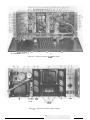
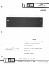
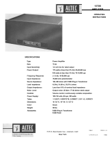
The Altec 1594B Power Amplifier delivers up to 100 watts of output power for various sound reinforcement systems. It features a switchable highpass filter to protect driver loudspeakers, and its Active Dissipation Sensing Circuit provides fail-safe protection for the output transistors. The 1594B is versatile, with transformer-isolated outputs for 4, 8 and 16 ohms, as well as for 25V and 70.7V distribution systems.
The Altec 1594B Power Amplifier delivers up to 100 watts of output power for various sound reinforcement systems. It features a switchable highpass filter to protect driver loudspeakers, and its Active Dissipation Sensing Circuit provides fail-safe protection for the output transistors. The 1594B is versatile, with transformer-isolated outputs for 4, 8 and 16 ohms, as well as for 25V and 70.7V distribution systems.


-
 1
1
-
 2
2
-
 3
3
-
 4
4
-
 5
5
-
 6
6
-
 7
7
-
 8
8
-
 9
9
-
 10
10
-
 11
11
-
 12
12
-
 13
13
-
 14
14


Altec 1594B Operating Instructions Manual
- Type
- Operating Instructions Manual
The Altec 1594B Power Amplifier delivers up to 100 watts of output power for various sound reinforcement systems. It features a switchable highpass filter to protect driver loudspeakers, and its Active Dissipation Sensing Circuit provides fail-safe protection for the output transistors. The 1594B is versatile, with transformer-isolated outputs for 4, 8 and 16 ohms, as well as for 25V and 70.7V distribution systems.
Ask a question and I''ll find the answer in the document
Finding information in a document is now easier with AI
Related papers
Other documents
-
 Altec Lansing 1590E User manual
-
Bogen MT250D User manual
-
 Altec Lansing 9860A Operating Instructions Manual
-
Audioplex The Beast Installation guide
-
Shure SR105A User manual
-
 Altec Lansing 1570B Operating instructions
-
-
-
-
Electro-Voice U192 Operating instructions


