
UM10377
STARplug Universal SO14 and DIP8 demo boards
Rev. 2 — 20 July 2011 User manual
Document information
Info Content
Keywords STARplug, SMPS, flyback converter
Abstract The NXP Semiconductors STARplug Universal demo board comes in two
versions: one with an SMD SO14 STARplug IC mounted and one with a
through-hole DIP8. The flyback converter demo board is highly flexible
and can be configured for isolated and non-isolated operation. Multiple
output configurations and feedback schemes can be achieved on the
PCB.
The default board comes as an isolated SMPS which provides two DC
output voltages: 12 V and 5 V. The nominal power that can be drawn from
the board is 8 W.
This manual describes the SO14 and the DIP8 variants of the STARplug
Universal demo board version 1.11. Refer to the TEA152x and TEA162x
data sheets for details on the STARplug device and the STARplug
application note AN00055 for general application information.

UM10377 All information provided in this document is subject to legal disclaimers. © NXP B.V. 2011. All rights reserved.
User manual Rev. 2 — 20 July 2011 2 of 36
Contact information
For more information, please visit: http://www.nxp.com
For sales office addresses, please send an email to: [email protected]
NXP Semiconductors
UM10377
STARplug Universal SO14 and DIP8 demo boards
Revision history
Rev Date Description
v.2 20110720 second issue
v.1 20100407 first issue

UM10377 All information provided in this document is subject to legal disclaimers. © NXP B.V. 2011. All rights reserved.
User manual Rev. 2 — 20 July 2011 3 of 36
NXP Semiconductors
UM10377
STARplug Universal SO14 and DIP8 demo boards
1. Introduction
The STARplug Universal Switched Mode Power Supply (SMPS) demo board described in
this user manual, provides two DC output voltage levels: 12 V and 5 V. Fundamentally, the
two output voltages are galvanically isolated enabling the 12 V and 5 V outputs to be
combined in an arbitrary way (see Section 2
). In the default configuration, the 12 V and
5 V outputs are galvanically connected using a common GND (0 V). The board has a
universal mains input and the total nominal output power is rated at 8 W.
Non-continuous/peak output power levels of up to 12 W are also supported in the default
configuration.
The flyback circuit is built around the TEA1522 STARplug IC. On the STARplug Universal
demo board there are several provisions to enable reconfiguration such as input filtering,
snubber circuit, output voltage configuration, regulation feedback scheme and more. The
STARplug Universal demo board can be used both in isolated and non-isolated mode. In
addition, with the DIP8 version of the STARplug Universal, you can easily swap the
STARplug IC, as the IC is mounted in an IC socket.
Small changes in the output voltage (up to 20 %) are also supported but the ratio
between the first and the second output voltage remains unaltered. If an alternative
transformer is considered, the Printed-Circuit Board (PCB) can be used to generate any
output voltage and output voltage combination. These features make the STARplug
Universal demo board highly versatile. This versatility requires some PCB space.
Therefore this board is not intended as a showcase for minimal PCB space consumption
and it is by no means an end solution. It is, however, very useful for exploring all the board
features and the features of the STARplug family of ICs during development of a final
solution for an isolated or non-isolated low power SMPS application.
WARNING
Lethal voltage and fire ignition hazard
The non-insulated high voltages that are present when operating this product, constitute a
risk of electric shock, personal injury, death and/or ignition of fire.
This product is intended for evaluation purposes only. It shall be operated in a designated test
area by personnel qualified according to local requirements and labor laws to work with
non-insulated mains voltages and high-voltage circuits. This product shall never be operated
unattended.

UM10377 All information provided in this document is subject to legal disclaimers. © NXP B.V. 2011. All rights reserved.
User manual Rev. 2 — 20 July 2011 4 of 36
NXP Semiconductors
UM10377
STARplug Universal SO14 and DIP8 demo boards
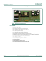
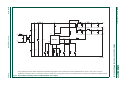
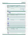
a. SO14 demo board
b. DIP8 demo board
Fig 1. STARplug Universal demo boards
019aab935
019aab936

UM10377 All information provided in this document is subject to legal disclaimers. © NXP B.V. 2011. All rights reserved.
User manual Rev. 2 — 20 July 2011 5 of 36
NXP Semiconductors
UM10377
STARplug Universal SO14 and DIP8 demo boards
1.1 Features
• Universal mains input
• Operates in isolated and non-isolated mode
• Two default DC output voltages: 12 V and 5 V
• Very stable regulated voltage
• User selectable output voltage configuration
• Highly flexible and easily tunable to user requirements
• Supports the TEA152x and TEA162x family of ICs (except the TEA1623PH)
• 8 W nominal output power, 12 W peak/maximum
• High-efficiency: > 80 %
• Low standby (no-load) power: < 80 mW
• Overload protection
• OverTemperature Protection (OTP)
• Built-in ElectroMagnetic Interference (EMI) filter
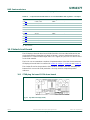
Fig 2. STARplug Universal demo board
019aac319

UM10377 All information provided in this document is subject to legal disclaimers. © NXP B.V. 2011. All rights reserved.
User manual Rev. 2 — 20 July 2011 6 of 36
NXP Semiconductors
UM10377
STARplug Universal SO14 and DIP8 demo boards
2. Safety warning
This reference board is connected to a high AC voltage (up to 276 V). Touching the demo
board during operation must be avoided at all times. An isolated housing is obligatory
when used in uncontrolled, non laboratory environments. Galvanic isolation of the mains
phase using a fixed or variable transformer (Variac) is always recommended. These
devices can be recognized by the symbols shown in Figure 3
3. Technical specification
4. Performance data
4.1 Output voltage and no-load power consumption
Table 3 shows the no-load power consumption figures for the default configuration of the
STARplug Universal demo board.
a. Isolated b. Not isolated
Fig 3. Variac isolation symbols
019aab173
019aab174
Table 1. Input specification
Parameter Condition Value Remark
Input voltage - 90 V (AC) to 276 V (AC) universal mains
Input frequency - 47 Hz to 63 Hz -
Table 2. Output specification
Output supply Condition Value Remark
Output voltage 1 - 12 V default configuration: regulated output
Output voltage 1 tolerance at 75 % load 2% -
Output voltage 1 stability - 2 % over full power range
Output voltage 2 - 5 V default configuration: non-regulated
Output voltage 2 tolerance - - dependent on the output 1 load
Output voltage 2 stability - -
Table 3. No-load output voltage and power consumption
Supply Energy star 2.0
requirement
Output voltage 1 Power consumption
(P
o
)
115V/60Hz 300 mW 11.9 V 75 mW
230 V/50 Hz 300 mW 11.9 V 75 mW

UM10377 All information provided in this document is subject to legal disclaimers. © NXP B.V. 2011. All rights reserved.
User manual Rev. 2 — 20 July 2011 7 of 36
NXP Semiconductors
UM10377
STARplug Universal SO14 and DIP8 demo boards
Remark: Output voltage 2 can vary considerably when no-load is connected because this
output voltage is not regulated in the default configuration.
4.2 Efficiency performance data
Table 4 shows the efficiency figures for the default configuration of the STARplug
Universal demo board.
The following conditions apply:
• The rated nominal output power at both 115 V (AC) and 230 V (AC) is 8 W
• The load is on the 12 V output only
• Warm-up time of 15 minutes, settle time after load change is 90 s
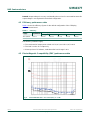
4.3 ElectroMagnetic Compatibility (EMC) performance data
Table 4. Efficiency
Power
supply
Energy star
requirement
Efficiency ()
average 25 % load 50 % load 75 % load 100 % load
115V/60Hz 75.2% 81.1% 81.4% 81.5% 81.1% 80.2%
230 V/50 Hz 75.2 % 81.2 % 79.3 % 81.6 % 82.1 % 82.0 %
Fig 4. Conducted EMC test: V
IN
= 115 V (AC), P
o
= 6 W
019aab937

UM10377 All information provided in this document is subject to legal disclaimers. © NXP B.V. 2011. All rights reserved.
User manual Rev. 2 — 20 July 2011 8 of 36
NXP Semiconductors
UM10377
STARplug Universal SO14 and DIP8 demo boards
Remark: Both the average and quasi-peak EMC performance of the STARplug Universal
demo board meet EN55022.
Fig 5. Conducted EMC test: V
IN
= 230 V (AC), P
o
= 6 W
019aab938

UM10377 All information provided in this document is subject to legal disclaimers. © NXP B.V. 2011. All rights reserved.
User manual Rev. 2 — 20 July 2011 9 of 36
NXP Semiconductors
UM10377
STARplug Universal SO14 and DIP8 demo boards
5. Demo board connections
Remark: Reversing the live and neutral connections has no influence on the practical
operation of the STARplug Universal demo board.
Terminals J3 and J4 produce 12 V (J3 positive with respect to J4). The combination of J5
and J6 produces 5 V (J5 positive with respect to J6). In the default configuration, J4 is
connected to J6 by means of a wire bridge (G to K) on the output configuration block. In
alternative configurations, the pairs (J3, J4) and (J5, J6) could be used completely
independently or even floating.
Fig 6. Demo board connection set-up
019aab939
live (J2)
neutral (J1)
12 V (J3)
GND (J4)
5 V (J5)
GND (J6)

UM10377 All information provided in this document is subject to legal disclaimers. © NXP B.V. 2011. All rights reserved.
User manual Rev. 2 — 20 July 2011 10 of 36
NXP Semiconductors
UM10377
STARplug Universal SO14 and DIP8 demo boards
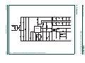
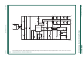
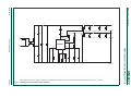
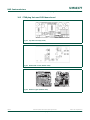
6. Circuit description
The default STARplug Universal SMPS demo board consists of a single-phase full-wave
rectifier circuit, a filtering section, a switching section, an output section and a feedback
section.
The full circuit diagram of the default configuration of the STARplug Universal demo board
PCB, including the connections (A to K) on the output configuration block, is shown in
Figure 7
.
The STARplug Universal demo board comes with wire bridges A to D, C to E, D to G and
G to K installed as the default. This results in an SMPS with 12 V and 5 V output that
shares a common GND. Regulation in this case is only on the 12 V output. Figure 8
shows the relevant electrical circuit diagram.
6.1 Rectification section
The single-phase full-wave rectifier consists of four individual diodes (D1 to D4) in a
Greatz bridge configuration. The reason for using four individual diodes instead of a single
diode bridge component is purely practical. If the STARplug Universal demo board is used
with half-wave rectification, it is easy to create a PCB populated with just one diode (D1).
See Section 7.8
for details.
Capacitor C3 functions as a reservoir capacitor for the rectified input voltage. Inrush
current is limited by resistor R1. This resistor must be a carbon resistor and not a metal
film resistor because a metal film type resistor could work as a fuse instead of an inrush
current limiter.
Terminals J1 and J2 connect the input to the electricity utility network. J1 is referred to as
neutral and J2 as live for convenience. Swapping these two wires has no effect on the
operation of the STARplug Universal converter.
6.2 Filtering section
The filtering section consists of the common-mode choke L1 and C1 on the AC side of the
diode bridge and C3, L2 and C4 in -configuration on the DC side. If, in exceptional
circumstances additional noise suppression is needed, Surface Mounted Device (SMD)
capacitors C2 and C5 can be added in parallel to the electrolytic capacitors C3 and C4.
The whole filtering configuration effectively reduces the noise and harmonic content that
would otherwise be injected from the TEA1522 switching electronics into the electricity
utility network. The circuitry helps to achieve the EMC performance required by EN55022.
6.3 Switching section
The switching section uses an NXP Semiconductors STARplug TEA1522 IC in either a
SO14 or DIP8 package (depending on the board version). The operating frequency is set
using the combination of R2 and C6.
The parallel circuit of resistors R5, R5B and R5C limit the peak current that occurs in the
STARplug internal MOSFET switch and as a consequence in the primary winding of
transformer T1. The current limitation simultaneously prevents the internal MOSFET
switch from being overstressed and it implements an overload protection of the SMSP
output. The maximum switch current is shown in Equation 1
.

UM10377 All information provided in this document is subject to legal disclaimers. © NXP B.V. 2011. All rights reserved.
User manual Rev. 2 — 20 July 2011 11 of 36
NXP Semiconductors
UM10377
STARplug Universal SO14 and DIP8 demo boards
(1)
The supply voltage for the TEA1522 IC is generated by an auxiliary winding on
transformer T1. The voltage from the auxiliary winding (half-wave) is rectified by diode D7.
Capacitor C8 is charged via the current limiter resistor R8. The voltage on C8 is the supply
voltage for the TEA1522 V
CC
pin. The AUX pin of the IC receives information regarding
the magnetization status of transformer T1 via resistor R6.
A snubber circuit which handles voltage spikes and associated energy caused by the
leakage inductance of the primary winding of transformer T1 is implemented using a
diode-Zener snubber (D5 and D6). This type of snubber conserves energy and is EMI
friendly but it is also a more expensive option compared to an RCD snubber (see
Section 7.2
).
6.4 Output section
The output section of the STARplug Universal application produces two DC voltages: 12 V
and 5 V. The 12 V section consists of diode D9, capacitors C10, C12, C13 and inductor
L3. The 5 V section consists of diode D6, capacitors C11, C14, C15 and inductor L4.
The output sections provide a good level of ripple filtering and noise suppression by using
-configurations in both the 12 V and the 5 V section. In the default configuration, the
GND terminals of the 12 V and the 5 V supplies are tied together. J4 and J6 are GND
(0 V), J5 is +5 V and J3 is +12 V.
6.5 Feedback section
The feedback signal is taken from the 12 V supply but it can be changed to either the 5 V
supply or a weighed combination of the 12 V and 5 V supplies (see Section 7.4
).
In the default configuration, the feedback network on the secondary side consists of
resistors R18, R17, R16; capacitors C18, C19, and voltage reference IC3 (TL431A).
Resistors R18 and R17 form a voltage divider and determine the output voltage of the
(12 V) supply. The programmed output voltage (12 V output terminal J3) is calculated
using Equation 2
.
(2)
V
REG
is the reference voltage of IC3 and for a TL431 this voltage is 2.5 V. R13 and C17
provide the supply power for the feedback network and R14 functions as a current limiter
for the LED in the optocoupler IC2. The feedback signal is transferred across the isolation
barrier through optocoupler IC2. On the primary side, the signal is fed to the TEA1522
REG pin via the current limiting resistor R7. When the optocoupler is in the off-state, the
REG pin is pulled down by resistor R10, noise is filtered and a pole is added with
capacitor C9. Zener diode D8 protects against the optocoupler failing (e.g. through
ageing). In this case, the generated output voltage is limited by Zener diode D8 instead of
rising in an uncontrolled way.
Remark: Refer to the STARplug TEA152x data sheet, the TEA162x data sheet and the
STARplug application note AN00055 for more detailed/accurate information on the
operation of STARplug TEA152x/TEA162x ICs and dimensioning of STARplug circuits.
I
DS max
0.5
R5//R5B//R5C
-------------------------------------
=
V
out_12V
V
REG
R17 R18+
R17
--------------------------
=

UM10377 All information provided in this document is subject to legal disclaimers. © NXP B.V. 2011. All rights reserved.
User manual Rev. 2 — 20 July 2011 12 of 36
NXP Semiconductors
UM10377
STARplug Universal SO14 and DIP8 demo boards
7. Alternative circuit options
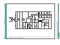
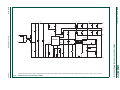
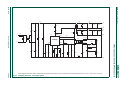
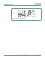
7.1 Additional filtering capacitors in the rectification/filtering sections
In exceptional cases, two additional SMD capacitors (C2 and C5) placed in parallel to the
electrolytic capacitors C3 and C4 help to suppress the EMI even more. See the circuit
diagram shown in Figure 10
and the component changes given in Table 9.
7.2 Alternative snubber circuit
The D5/D6 diode-Zener snubber is usually a good solution for snubbering the leakage
energy of the primary winding of the transformer. However, a cheaper RCD solution is
sometimes preferred. The STARplug Universal demo board has a provision that allows
the mounting of an RCD snubber circuit (D5, C7, R3, R4) instead of a diode-Zener
snubber. The resistor “R” part of the RCD is split in two. The power dissipation and voltage
drop is divided equally over these standard (1206 sized) SMD resistors.
The circuit diagram shown in Figure 11
and the component changes given in Table 10
describe the STARplug Universal application using a RCD snubber.
7.3 Primary feedback
The STARplug Universal demo board allows the implementation of primary feedback
schemes in an isolated SMPS application. This feature is intended, for example, in low
output power applications. The consequence of the primary feedback option when
implemented on this board is that voltage regulation is (much) less accurate. However, as
a trade-off, the cost savings can be significant.
To ensure reasonably good voltage regulation, it is essential that the magnetic coupling
between the secondary winding and the auxiliary winding of the transformer is very good.
This requirement can add considerable cost because of the transformer construction.
The circuit diagram shown in Figure 12
and the component changes given in Table 11
indicate that the circuit diagram is simplified and the parts list is shorter.
7.4 Alternative secondary side feedback
In the default configuration, only the 12 V rail of the STARplug Universal demo board is
regulated. It can be desirable to regulate the 5 V output or a (weighted) combination of the
12 V and 5 V output depending on the application.
When regulation of only the 5 V output voltage is required, resistor R18 is removed from
the PCB (set to ) and wire bridge B to H is installed in the output configuration block.
The output voltage produced on the 5 V output terminals (J5, J6) is given in Equation 3
.
The 12 V output voltage on terminals (J3, J4) are now unregulated.
(3)
When a weighed combination of the 12 V and the 5 V output is regulated, the ratio (V
ratio
)
between the 12 V and the 5 V output is fixed by a factor of .
V
out_5V
V
REG
R17 R20+
R20
--------------------------
=
V
ratio
12 5 2.4==

UM10377 All information provided in this document is subject to legal disclaimers. © NXP B.V. 2011. All rights reserved.
User manual Rev. 2 — 20 July 2011 13 of 36
NXP Semiconductors
UM10377
STARplug Universal SO14 and DIP8 demo boards
The only way to change this factor is by modifying the turns ratio on the secondary side of
the T1 transformer. Both resistors R18 and R20 are affected in this case and their values
need to be changed. Both wire bridges B to H and C to E must be installed. The
mathematical expression for the (weighed) regulation on two output voltages is more
complex than the expressions that apply to regulation on a single output voltage. The
expression for weighed regulation is given in Equation 4
and Equation 5.
(4)
(5)
In the default STARplug Universal demo board configuration, V
REG
= 2.5 V (IC2 TL431
reference voltage) and V
ratio
= 2.4 (i.e. the turns ratio between the 12 V and 5 V output on
the secondary winding of transformer T1).
It can be seen that Equation 4
and Equation 5 transform into Equation 2 when R20 is
removed (i.e. R20 = ) and that they transform into Equation 3
when R18 is removed
(i.e. R18 = ).
When an SMPS application with output voltages 12 V and 5 V is designed, the balance
between the values of R18 and R20 determines the weight that each of the output
voltages has on the regulation. The weighting of the feedback regulation contribution of
either voltage rails is given in Equation 6
and Equation 7.
(6)
(7)
Table 5
gives an overview of various R18 and R20 resistor combinations and weighting
factors. R17 is left at its default value of 2.4 k.
Table 5. R17, R18 and R20 exact component values for weighed regulation
Output weighting Resistor values
5V 12 V R17 R18 R19
0 % 100 % 2.4 k 9.12 k
5% 95% 2.4k 9.60 k 48.00 k
10 % 90 % 2.4 k 10.13 k 24.00 k
20 % 80 % 2.4 k 11.40 k 12.00 k
30 % 70 % 2.4 k 13.03 k 8.00 k
50 % 50 % 2.4 k 18.24 k 4.80 k
70 % 30 % 2.4 k 30.4 k 3.43 k
80 % 20 % 2.4 k 45.6 k 3.00 k
90 % 10 % 2.4 k 91.2 k 2.67 k
95 % 5 % 2.4 k 182.4 k 2.53 k
100% 0% 2.4k 2.40 k
V
out_12V
V
REG
R17 R18 R17 R20 R18 R20++
R17 R20 R17
R18
V
ratio
--------------
+
-------------------------------------------------------------------------------------------
=
V
out_5V
V
out_12V
V
ratio
--------------------
=
Weight V
out_12V
R17
R18
----------
V
out_12V
V
REG
–
V
REG
----------------------------------------
100 %=
Weight V
out_5V
R17
R20
----------
V
out_5V
V
REG
–
V
REG
-------------------------------------
100 %=

UM10377 All information provided in this document is subject to legal disclaimers. © NXP B.V. 2011. All rights reserved.
User manual Rev. 2 — 20 July 2011 14 of 36
NXP Semiconductors
UM10377
STARplug Universal SO14 and DIP8 demo boards
Table 5 lists a number of R18 and R20 resistance values that are not practical and
generally, the regulation balance does not need to be defined so precisely. Table 6
lists a
number of R17, R18, R20 combinations that are more practical, whilst keeping the idea of
weighed regulation. The resistance values come from the E24 range. Small deviations
(1 %) in the output voltages are acceptable.
Remark: The circuit corresponding to these alternative (weighed) secondary feedback
values is shown in Figure 13
. See Table 12 for the component changes involved.
7.5 Alternative output configurations
The output configuration block is used for selecting the output voltage configuration using
wire bridges. In the default configuration, the output voltage is set to +12 V and +5 V (with
regulation/feedback on the 12 V): +12 V on J3, +5 V on J5, 0 V on J4 and J6. This is
achieved by inserting the wire bridges in the output configuration block between columns
A and D, C and E, D and G, and G and K.
Screw terminal positions J3, J4, J5 and J6 are shown in Figure 6
and the default wire
bridges in the output configuration block are shown in Figure 7
. See Figure 17 and
Figure 21
for an overview of the position of terminals and wire bridges.
Table 7 gives a series of output configurations that can be made by setting the wire
bridges in the output configuration block. The list of Table 7
is not extensive because the
number of configuration possibilities is very large. By carefully studying the circuit diagram
in Figure 8
, the user can to see how customized output configurations can be made.
Table 6. Practical R17, R18 and R20 exact component values for weighed regulation
Resistor values output weighting 5V
o
12 V
o
R17 R18 R20 5V 12 V
2.4 k 9.1 k 0% 100% 5.0V 12.0V
2.7 k 11 k 43 k 6% 94% 5.0V 12.0V
2.4 k 10 k 24 k 10 % 90 % 5.0 V 11.9 V
2.7 k 13 k 13 k 21 % 79 % 5.0 V 12.0 V
2.4 k 13 k 8.2 k 29 % 71 % 5.0 V 12.1 V
2.7 k 20 k 5.6 k 49 % 51 % 5.0 V 12.0 V
2.4 k 33 k 3.3 k 72 % 28 % 5.0 V 12.0 V
2.4 k 47 k 3k 81 % 19 % 5.0 V 12.0 V
2.4 k 82 k 2.7 k 89 % 11 % 5.0 V 12.0 V
2.2 k 100 k 2.4 k 92 % 8 % 5.0 V 12.0 V
2.4 k 2.4 k 100 % 0 % 5.0 V 12.0 V
Fig 7. Default wire bridge settings for +12 V and +5 V output configuration block
019aab940
Output
configuration
block
ABCDEFGHJK

UM10377 All information provided in this document is subject to legal disclaimers. © NXP B.V. 2011. All rights reserved.
User manual Rev. 2 — 20 July 2011 15 of 36
NXP Semiconductors
UM10377
STARplug Universal SO14 and DIP8 demo boards
[1] Regulated voltage.
7.6 Self-supplied TEA152x application
When a STARplug IC from the TEA152x family is applied on the STARplug Universal
demo board, there is an option which enables the SMPS IC to generate its own power
supply using the built-in JFET. This is not available with TEA162x IC because these ICs
do not have the built-in JFET. The advantage of this is that the auxiliary winding on
transformer T1 is no longer needed reducing the cost.
The disadvantage is that generating the supply voltage through the built-in JFET causes
an additional power loss. Therefore the high-efficiency figures and low standby figures as
shown in Table 3
and Table 4 no longer apply.
Apart from supplying the V
CC
power for the STARplug IC, the auxiliary winding on the
transformer also informs the IC’s AUX pin about the magnetization status of the
transformer. When the auxiliary winding is no longer present, an alternative method is
needed to inform the AUX pin about the magnetization status of the transformer. This can
be done by capacitive coupling.
As the “hot” connections of the respective windings of the transformer T1 are in phase
during operation, the voltage (or information) on the “hot” side of the primary winding can
be used to indicate whether or not the transformer is demagnetized. Creating a capacitive
coupling between the “hot” side of the primary winding and the STARplug IC AUX pin
makes it easy to transfer this information.
Table 7. Examples of STARplug Universal output configuration in isolated mode
Supply STARplug Universal output configuration Modification Configuration block wire
jumpers
J3 J4 J5 J6 Regulation
+12V/+5V +12V 0V +5V 0V on +12V
[1]
default configuration A to D, C to E, D to G, G to K
+12V/+5V +12V 0V +5V 0V on +5V
[1]
remove R18 A to D, B to H, C to E, D to G,
GtoK
+12 V/5V +12V 0V 0V 5V on +12V
[1]
- A to D, C to E, D to G, G to J
+12 V/5V +12V 0V 0V 5V on 5V
[1]
remove R18, R13 = 1 k A to K, B to C, C to H, D to G,
GtoJ
+5 V/12 V 0 V 12V +5V 0V on 12 V
[1]
- A to G, C to E, F to K, D to K
+5 V/12 V 0 V 12V +5V 0V on +5V
[1]
remove R18, R13 = 1 k A to K, B to C, C to H, F to K,
DtoK
+17 V/+12 V +12 V 0 V +17 V +12 V on +12 V
[1]
- A to D, C to E, D to G, F to K
+17 V/+12 V +12 V 0 V +17 V +12 V
[1]
on +17V R18=18k,
R20 = 62 k,
R13=3.3k
A to D, B to C, C to H, D to G,
FtoK
+17V/+5V +17V +5V +5V 0V on +5V
[1]
remove R18, R13 = 1 k A to D, A to K, B to C, C to H,
GtoJ
+17V/+5V +17V +5V +5V 0V on +17V
[1]
R18 = 18 k,
R20 = 62 k,
R13=3.3k
A to D, A to K, G to J, B to C,
EtoC
+7 V/5V +7V 5V 0V 5V on 5V
[1]
remove R18, R13 = 1 k A to K, B to C, C to H, D to J,
GtoK
+7 V/5V +7V 5V 0V 5V on +7V
[1]
R20=8.2k,
R13=1.5k
A to H, B to C, C to E, D to J,
GtoK

UM10377 All information provided in this document is subject to legal disclaimers. © NXP B.V. 2011. All rights reserved.
User manual Rev. 2 — 20 July 2011 16 of 36
NXP Semiconductors
UM10377
STARplug Universal SO14 and DIP8 demo boards
A small capacitive coupling is enough because of the relatively high-impedance of the
AUX pin. To guarantee that during start-up the voltage on the AUX pin is below 100 mV,
the pin must be pulled to ground using a high-ohmic resistor (around 500 k).
The capacitor is shown as C21 in Figure 14
acts as the capacitive coupler between the
transformer “hot” side and the STARplug IC AUX pin. A typical value for this capacitor is
2 pF. Therefore the parasitic capacitance that can be created with the layout of the PCB is
generally adequate to create sufficient coupling. Usually there is no need to mount the
C21 capacitor.
The ~500 k impedance between the IC AUX pin and GND is split in two resistor values,
R6 and R11. R6 limits the current that can be injected into the AUX pin through the
capacitive coupling (100 k typical). Overcurrent into the AUX pin may damage the IC.
The combination of R6 and R11 builds the impedance that pulls the AUX pin to ground
during start-up (R11 = 390 k typical).
When the STARplug IC is self-supplying via the built-in JFET, there is no longer any need
for Zener diode D8 because the V
CC
voltage will never rise high enough. This also means
the protection described in Section 6.5
is no longer active. A defective or strongly
degraded optocoupler IC2 results in an uncontrolled rise of the output voltage(s) of the
SMPS.
See Table 13
for the component changes involved.
7.7 Non-isolated SMPS application with a regulated +12 V output
If an non-isolated SMPS is designed with a regulated +12 V (DC) output, the STARplug IC
supply voltage (V
CC
) can be delivered by the secondary side of the transformer. The
transformer does not need an auxiliary winding. In addition, the demagnetization
information supplied to the AUX pin can also be delivered by the secondary side of the
transformer. Voltage information feedback via the voltage reference (IC3) and an
optocoupler (IC2) is no longer needed.
Wire bridges “Non-iso Dmg2” and “Non-iso FB1” must be installed, and Y-capacitor C16
must be replaced with a wire bridge (“Non-iso GND"). See Figure 17
and Figure 21 for the
locations of these wire bridges.
The 5 V output voltage supply section can either be used to generate +5 V, 5V, or +17V,
by installing the correct wire bridges in the output configuration block. The configuration
shown in Figure 15
produces +12 V (on J3) and +5 V (on J5), while J4 and J6 are tied
together at 0 V (GND) level. Only implement this option when there is no auxiliary winding
on the transformer or when the auxiliary winding of the transformer has no galvanic
connection to resistor R6 (e.g. by cutting the appropriate transformer pin).
The circuit diagram shown in Figure 15
and the component changes given in Table 14
describe the non-isolated STARplug Universal application with a regulated +12 V output.
7.8 Non-isolated SMPS application with a regulated 5 V output
If a non-isolated SMPS application that has a regulated 5 V (DC) output is designed, the
STARplug IC supply voltage (V
CC
) must be delivered either by the auxiliary winding of the
transformer or using the self-supply option of the TEA152x IC (see Section 7.6
). The
demagnetization information can be supplied either by the auxiliary winding (preferred, if
present) or through capacitive coupling as described in Section 7.6
.

UM10377 All information provided in this document is subject to legal disclaimers. © NXP B.V. 2011. All rights reserved.
User manual Rev. 2 — 20 July 2011 17 of 36
NXP Semiconductors
UM10377
STARplug Universal SO14 and DIP8 demo boards
Voltage information feedback via an optocoupler (IC2) is not needed but the negative
output voltage must be translated into a control signal for the STARplug IC REG pin. This
is done with a circuit consisting of an NPN transistor (Q2), a PNP transistor (Q1), a Zener
diode (D12) and a few passive components.
In this example, the demagnetization information is provided by the auxiliary winding of
the transformer. Wire bridge “Non-iso FB2” must be installed and Y-capacitor C16 must
also be replaced with a wire bridge (“Non-iso GND”). See Figure 17
and Figure 21 for the
locations of these wire bridges.
The 12 V output voltage supply section can be used to either generate +12 V, +7 V, or
17 V or as a fully independent (floating) 12 V supply voltage. All the options can be
achieved by installing the appropriate wire bridges in the output configuration block.
The configuration shown in Figure 16
produces 5 V on J6 (and J4), +7 V on J3 and 0 V
(GND) on J5. J4 and J6 are tied together and are at the 5 V level. The input rectification
stage in this example is a half-wave rectifier that uses a single diode (D1). The
common-mode input filter (L1, C1) is eliminated. This makes it possible to have the
neutral wire from the mains (terminal J1) connected to the 0 V (GND) level of the output
stage (terminal J5). This is especially useful for applications using a 5 V supply to drive
triacs in the third quadrant (such as most White Goods applications).
The circuit diagram shown in Figure 16
and the component changes given in Table 15
describe the non-isolated STARplug Universal application with a regulated 5 V output.
7.9 Combining options and features
Options and features can be combined as described in Section 7 to Section 7.8. A new
combination of options and features need to be checked so that the specific combination
does not cause an electrical conflict. If needed, contact NXP Semiconductors application
support for additional application help.

xxxx xxxxxxxxxxxxxxxxxxxxxxxxxxxxxx x xxxxxxxxxxxxxx xxxxxxxxxx xxx xxxxxx xxxxxxxxxxxxxxxxxxxxxxx xxxxxxxxxxxxxxxxxxxxxx
xxxxx xxxxxx xx xxxxxxxxxxxxxxxxxxxxxxxxxxxxx xxxxxxxxxxxxxxxxxxxxxx xxxxxxxxxxx xxxxxxx xxxxxxxxxxxxxxxxxxx
xxxxxxxxxxxxxxxx xxxxxxxxxxxxxx xxxxxx xx xxxxxxxxxxxxxxxxxxxxxxxxxxxxxxxx xxxxxxxxxxxxxxxxxxxxxxxx xxxxxxx
xxxxxxxxxxxxxxxxxxxxxxxxxxxxxxxxxxxxxxxxxxxxxx xxxxxxxxxxx xxxxx x x
UM10377 All information provided in this document is subject to legal disclaimers. © NXP B.V. 2011. All rights reserved.
User manual Rev. 2 — 20 July 2011 18 of 36
NXP Semiconductors
UM10377
STARplug Universal SO14 and DIP8 demo boards
8. Schematics
Fig 8. STARplug Universal with output configuration block connections shown
019aab941
L1
L2
R1
R7
C16
R16
R14 R20
R18
R13
C
J6
J5
J4
J3
B
A
D
C19
C18
C1
C6
IC1
C9
C17 R17
C8
D8
D7
D9
E
D10
IC2
D5
D6
R5C
C3
C4
C10
C11
C12
C14
C13
C15
R2
R5A
R5B
R10
IC3
R6
R8
SOURCE
REG
DRAIN
RC
GND
J2
J1
TEA152x
D2
D4
T1
AUX
V
CC
D1
D3
L3
L4
H
F
J
G
K

xxxxxxxxxxxxxxxxxxxxx xxxxxxxxxxxxxxxxxxxxxxxxxx xxxxxxx x x x xxxxxxxxxxxxxxxxxxxxxxxxxxxxxx xxxxxxxxxxxxxxxxxxx xx xx xxxxx
xxxxxxxxxxxxxxxxxxxxxxxxxxx xxxxxxxxxxxxxxxxxxx xxxxxx xxxxxxxxxxxxxxxxxxxxxxxxxxxxxxxxxxx xxxxxxxxxxxx x x
xxxxxxxxxxxxxxxxxxxxx xxxxxxxxxxxxxxxxxxxxxxxxxxxxxx xxxxx xxxxxxxxxxxxxxxxxxxxxxxxxxxxxxxxxxxxxxxxxxxxxxxxxx xxxxxxxx
xxxxxxxxxxxxxxxxxxxxxxxxx xxxxxxxxxxxxxxxxxxxx xxx
UM10377 All information provided in this document is subject to legal disclaimers. © NXP B.V. 2011. All rights reserved.
User manual Rev. 2 — 20 July 2011 19 of 36
NXP Semiconductors
UM10377
STARplug Universal SO14 and DIP8 demo boards
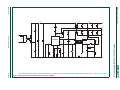
In the STARplug Universal default configuration the following wire bridges must be installed in the output configuration block: A to D; C to E; D to G and G to K.
Fig 9. STARplug Universal - default configuration
019aab942
L1
L2
R1
R7
C16
R16
R14
R18
R13
J6
J5
J4
J3
C19
C18
C1
C6
IC1
C9
C17 R17
C8
D8
D7
D9
D10
IC2
D5
D6
R5C
C3
C4
C10
C11
C12
C14
C13
C15
R2
R5A
R5B
R10
IC3
R6
R8
SOURCE
REG
DRAIN
RC
GND
J2
J1
TEA152x
D2
D4
T1
AUX
V
CC
D1
D3
L3
L4

xxxxxxxxxxxxxxxxxxxxx xxxxxxxxxxxxxxxxxxxxxxxxxx xxxxxxx x x x xxxxxxxxxxxxxxxxxxxxxxxxxxxxxx xxxxxxxxxxxxxxxxxxx xx xx xxxxx
xxxxxxxxxxxxxxxxxxxxxxxxxxx xxxxxxxxxxxxxxxxxxx xxxxxx xxxxxxxxxxxxxxxxxxxxxxxxxxxxxxxxxxx xxxxxxxxxxxx x x
xxxxxxxxxxxxxxxxxxxxx xxxxxxxxxxxxxxxxxxxxxxxxxxxxxx xxxxx xxxxxxxxxxxxxxxxxxxxxxxxxxxxxxxxxxxxxxxxxxxxxxxxxx xxxxxxxx
xxxxxxxxxxxxxxxxxxxxxxxxx xxxxxxxxxxxxxxxxxxxx xxx
UM10377 All information provided in this document is subject to legal disclaimers. © NXP B.V. 2011. All rights reserved.
User manual Rev. 2 — 20 July 2011 20 of 36
NXP Semiconductors
UM10377
STARplug Universal SO14 and DIP8 demo boards
In the STARplug Universal default configuration the following wire bridges must be installed in the output configuration block: A to D; C to E; D to G and G to K.
Fig 10. STARplug Universal with additional filtering
019aab943
L1
L2
R1
R7
C16
R16
R14
R18
R13
J6
J5
J4
J3
C19
C18
C1
C6
IC1
C9
C17 R17
C8
D8
D7
D9
D10
IC2
D5
D6
R5C
C3C2 C4 C5
C10
C11
C12
C14
C13
C15
R2
R5A
R5B
R10
IC3
R6
R8
SOURCE
REG
DRAIN
RC
GND
J2
J1
TEA152x
D2
D4
T1
AUX
V
CC
D1
D3
L3
L4
Page is loading ...
Page is loading ...
Page is loading ...
Page is loading ...
Page is loading ...
Page is loading ...
Page is loading ...
Page is loading ...
Page is loading ...
Page is loading ...
Page is loading ...
Page is loading ...
Page is loading ...
Page is loading ...
Page is loading ...
Page is loading ...
-
 1
1
-
 2
2
-
 3
3
-
 4
4
-
 5
5
-
 6
6
-
 7
7
-
 8
8
-
 9
9
-
 10
10
-
 11
11
-
 12
12
-
 13
13
-
 14
14
-
 15
15
-
 16
16
-
 17
17
-
 18
18
-
 19
19
-
 20
20
-
 21
21
-
 22
22
-
 23
23
-
 24
24
-
 25
25
-
 26
26
-
 27
27
-
 28
28
-
 29
29
-
 30
30
-
 31
31
-
 32
32
-
 33
33
-
 34
34
-
 35
35
-
 36
36


Ask a question and I''ll find the answer in the document
Finding information in a document is now easier with AI
Related papers
Other documents
-
Headphones R18 User manual
-
ON Semiconductor NCP1351 Series User manual
-
DKS 1812 - 12V 1A Power Transformer User manual
-
 Augustica Corvette User manual
-
 Augustica Frigate User manual
-
Lightolier C6TCAA User manual
-
Analog Devices EVAL-ADuM3070EBZ User manual
-
-
Cree TPAR20-0553040FH25-12DE26-1-11 User manual
-
Broadcom Evaluation Board for ACNW261L / ACNT-H61L Ultra Low Power 10MBd Digital CMOS Optocouplers User guide

