
© Semiconductor Components Industries, LLC, 2012
October, 2012 − Rev. 0
1 Publication Order Number:
EVBUM2150/D
NCP1351PRINTGEVB
NCP1351 16 V/32 V – 40 W
Printer Power Supply
Evaluation Board
User'sManual
Description
The present document describes a printer power supply
operated by the NCP1351, a fixed
t
on
/variable off time
controller. The board can deliver 10 W average on a 16 V
output and 30 W average on a 32 V output with a transient
peak power capability of 80 W. It however exhibits a low
standby power: below 150 mW at no load whatever the input
voltage. Let us first review the benefit of using the
NCP1351:
The NCP1351 at a Glance
Fixed t
on
, Variable t
off
Current-mode Control:
Implementing a fixed peak current mode control (hence
the more appropriate term “quasi-fixed” t
on
), the NCP1351
modulates the off time duration according to the output
power demand. In high power conditions, the switching
frequency increases until a maximum is hit. This upper limit
depends on an external capacitor selected by the designer. In
light load conditions, the off time expands and the NCP1351
operates at a lower frequency. As the frequency reduces, the
contribution of all frequency-dependent losses accordingly
goes down (driver current, drain capacitive losses, switching
losses), naturally improving the efficiency at various load
levels.
Peak Current Compression at Light Loads:
Reducing the frequency will certainly force the converter
to operate into the audible region. To prevent the transformer
mechanical resonance, the NCP1351 gradually reduces –
compresses – the peak current setpoint as the load becomes
lighter. When the current reaches 30% of the nominal value,
the compression stops and the off duration keeps expanding
towards low frequencies.
Low Standby-power:
The frequency reduction technique offers an excellent
solution for designers looking for low standby power
converters. Also, compared to the skip-cycle method, the
smooth off time expansion does not bring additional ripple
in no-load conditions: the output voltage remains quiet.
Natural Frequency Dithering:
The quasi-fixed t
on
mode of operation improves the EMI
signature since the switching frequency varies with the
natural bulk ripple voltage.
Extremely Low Start-up Current:
Built on a proprietary circuitry, the NCP1351 startup
section does not consume more than 10 mA during the
startup sequence. The designer can thus easily combine
startup time and standby consumption.
Overload Protection Based on Fault Timer:
Every designer knows the pain of building converters
where a precise over current limit must be obtained. When
the fault detection relies on the auxiliary V
CC
, the pain even
increases. Here, the NCP1351 observes the lack of feedback
current and starts a timer to countdown. At the end of its
charge, the timer either triggers an auto-recovery sequence
(auto-restart, B and D versions) or permanently latches-off
(A and C). On C and D versions the fault timer is started at
an output power corresponding to 60% of the maximum
deliverable power; to allow transient peak power delivery.
Latch Fault Input:
A dedicated input lets the designer externally trigger the
latch to build additional protections such as over-voltage
(OVP) or over-temperature (OTP).
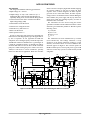
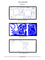
Figure 1. NCP1351 Evaluation Board
http://onsemi.com
EVAL BOARD USER’S MANUAL

NCP1351PRINTGEVB
http://onsemi.com
2
The Schematic
The design must fulfill the following specifications:
• Input Voltage: 88 – 265 Vac
• Output Voltage: 16 V @ 0.625 A and 32 V @ 1 A
Nominal (40 W); with Transient 80 W Peak Power
Capability during 40 ms, and 62 W Peak during 400 ms
• Over Power Protection below 100 W for the Whole
Input Voltage Range (LPS)
• Latched Short-circuit Protection
• Latched Over-voltage Protection
• Latch Recovery Time below 3 s
• Brown-out Protection
• Start-up Time below 3 s
In order to deliver the peak output power, the NCP1351
will increase its switching frequency up to the upper limit set
by the C
T
capacitor. To not jeopardize the EMI test
compliance, the switching frequency should be kept below
150 kHz. We will choose 100 kHz to have a good margin. As
a result the switching frequency at nominal load will be
around 50 kHz. Since we need to deliver 80 W of transient
peak power while ensuring the power will never be above
100 W, we will use the C version of NCP1351, specially
tailored for this kind of application. When the controller
detects a need for a frequency higher than 60 kHz, implying
an overload condition, it will start to charge the timer
capacitor: if the overload disappears, the timer capacitor
goes back to zero. If the fault remains, the timer capacitor
voltage reaches 5 V and latches off the controller. During the
fault condition, the power supply will anyway deliver the
output power while the switching frequency is below its
maximum value of 100 kHz.
The transformer has been derived using the Excel
®
spreadsheet available from the ON Semiconductor website
which also gives transformer parameters. We came up to the
following values:
L
p
= 270 mH
N
p
:N
s
= 1:0.2
N
p
:N
aux
= 1:0.2
I
pk
= 3 A
The transformer has been manufactured by Coilcraft
(www.coilcraft.com). The leakage inductance is kept
around 3% of the primary inductance, leading to a good
efficiency and reduced losses in no-load conditions. The
schematic appears on Figure 2. The converter operates in
DCM at nominal power; and
for peak power it goes CCM
with close to 50% duty-cycle at low mains and stays CCM
at high line.
X11
1
2
3
45
8
6
7
R1
C1
X4x
C4
R8
D3
C3
R10
R11
C8
C10
R13
R14
C12
D4
X6
C13
C14
D5
D7
C15
C16
L2
C17
C18
C19
L3
C20
R18
R19
R20
X4
X10
R21
R22
C21
Fuse
U1
R31
32 V
GND
16 V
C23
D11
R28
R30
Aux
D9
R15
D10
C6
R2
D13
R24
R23
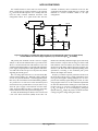
Figure 2. The Simplified 40 W Printer Board Featuring the NCP1351 Controller
+
+
+
+ +
+
L1
NCP1351C
R5
R6
C7
+

NCP1351PRINTGEVB
http://onsemi.com
3
Two 330 kW resistors in series with a 60 V zener diode
ensure a clean start-up sequence with the 4.7 mF capacitor
(C
3
), not from the bulk capacitor as it is usually done; but
from the fully rectified, unfiltered haversine. This
configuration allows for a quick release time after the
controller is latched (a direct connection to the AC line
would also work). Despite a small value for C
3
, the V
CC
still
maintains in no-load conditions thanks to the split
configuration:
1
2
3
4
5
8
6
7
HV rail
NCP1351
Aux
C7
D10
60 V
R5
330 k
R6
330 k
Figure 3. The split V
CC
configuration helps to start-up in a small period of time (C3 to charge alone)
but the addition of a second, larger capacitor (C7), ensures enough V
CC
in standby.
22 m
+
C3
+
4.7 m
C
bulk
+
V
CC
The primary-side feedback current is fixed to roughly
300 mA via R
8
and an additional bias is provided for the
TL431. 1 mA at least must flow in the TL431 in worse case
conditions (full load). Failure to respect this will degrade the
power supply output impedance and regulation will suffer.
A 2.7 kW value for R
19
has proven to do just well, without
degrading the standby power.
The overvoltage protection uses a 17 V zener diode (D
9
)
connected to the auxiliary V
CC
. When the voltage on this rail
exceeds 17 V plus the NCP1351 5 V latch trip point (total is
thus 22 V), the circuit latches-off and immediately pulls the
V
CC
pin down to 6 V. The reset occurs when the injected
current into the V
CC
pin falls below a few mA, that is to say
when the power supply is disconnected from the mains
outlet. To speed-up this reset phase, a connection to the fully
rectified haversine resets the system faster (Figure 3).
To satisfy the maximum power limit, we don’t need to add
a true Over Power Protection (OPP) circuit since our
NCP1351C transiently authorizes higher power, but safely
latches off if the overpower lasts too long. To ensure a fault
timer duration of at least 500 ms (to be able to deliver the
62 W power peak during 400 ms), the timer capacitor C10
must be 1.5 mF. This value will be adjusted depending on the
specification, according to the maximum peak power
duration the adapter must sustain.
If anyway a constant overpower protection is needed over
the whole input voltage range, a simple arrangement can be
used: given the negative sensing technique, we can use a
portion of the auxiliary signal during the on time, as it also
swings negative. However, we don’t want this compensation
for short T
ON
durations since standby power can be affected.
For this reason, we can insert a small integrator made of
C
9
−R
26
(see Figure 4). To avoid charging C
9
during the
flyback stroke, D
14
clamps the positive excursion and offers
a stronger negative voltage during the on time.

NCP1351PRINTGEVB
http://onsemi.com
4
Figure 4. A Simple Arrangement Provides an Adjustable Overpower Power Compensation
1
2
3
4
5
8
6
7
NCP1351
Vaux
++
V
CC
−N.Vin
R26
2.2 k
Rcomp
470 k
OPP Adjust
C9
220 p
D14
1N4148
Rcs
Rsense
A simple resistor connected between the auxiliary
winding (that swings negative during the ON time) and the
CT capacitor ensure a stable operation in CCM despite the
duty cycle above 50% at very low line, due to the ripple on
the bulk capacitor. The unique features of NCP1351C allow
using a 100 mF bulk capacitor while delivering the transient
peak power and ensuring the output is still regulated during
line drop-outs.
Finally, the clamping network maintains the drain voltage
below 520 V at high-line (375 Vdc) which provides 85%
derating for the 600 V BVdss device.
Measurements
Once assembled, the board has been operated during
15 min at full power to allow some warm-up time. We used
a WT210A from Yokogawa to perform all power related
measurements coupled to an electronic ac source.
Table 1. EFFICIENCY
V
IN
(P
OUT
) 120 Vac 230 Vac
40 W 84.4% 85.4%
25 W 85.9% 85.9%
10 W 86.0% 85.1%
5W 85.5% 83.2%
2W 83.4% 79.5%
1W 77.7% 73.3%
0.5 W 70.0% 66.3%
Table 2. NO-LOAD POWER
V
IN
(P
OUT
) 120 Vac 230 Vac
No-load 75 mW 140 mW
Overpower Protection Level:
The power supply is able to deliver a peak power of 85 W
during 500 ms from 85 Vac to 270 Vac.
It can deliver a constant output power of more than 40 W,
but less than 80 W over the same input voltage range.
Table 3. START-UP TIME
V
IN
(P
OUT
=40W) 85 Vac 230 Vac
Start-up Duration 2.7 s 0.5 s
In the above tables, we can see the excellent efficiency,
especially at light load conditions thanks to the natural
frequency foldback of the NCP1351.
The no-load standby power stays below 150 mW at high
line, a good performance for a dual output power supply able
to deliver 80 W. Please note that the high-voltage probe
observing the drain was removed and the load totally
disconnected to avoid leakage.
Despite operation in the audible range, we did not notice
any noise problems coming from either the transformer or
the RCD clamp capacitor.
V
in(min)
V
in(max)
0
20
40
60
80
100
120
020 6040 80 100 120 14
0
Figure 5. Switching Freq. Variations vs. Output Load
P
out
F
SW
CCM
Transition

NCP1351PRINTGEVB
http://onsemi.com
5
Scope Shots
Below are some oscilloscope shots gathered on the
evaluation board:
32 V
V
OUT
V
DRAIN
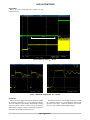
2.7 s
Figure 6. Start-up Time, V
IN
= 85 Vac
Figure 7. Maximum Output Power, V
IN
= 265 Vac
Conclusion
The printer power supply built with the NCP1351 exhibits
an excellent performance on several parameters like the
efficiency and the low-load standby. The transient switching
frequency increase allows to deliver peak power during a
limited time; but if the overpower lasts longer than the set
fault timer, the controller safely latches off.
The limited number of surrounding components around
the controller associated to useful features (timer-based
protection, latch input…) makes the NCP1351 an excellent
choice for cost-sensitive printer adapter designs.

NCP1351PRINTGEVB
http://onsemi.com
6
PCB LAYOUT
Figure 8. Top Side Components
Figure 9. Copper Traces
Figure 10. SMD Components

NCP1351PRINTGEVB
http://onsemi.com
7
X11
IRFIB6N60
1234
5867
R1
15
C1
100 n
R5
330 k
R6
330 k
R7
0
X4x
OptoBase
C4
R8
C5NC
D3
BAS20
C7
R10
1 k
R11
1 k
C8
10 n
C10
100 n
R133.4 k
R14
0.33
C12
10 n
D4
1N4007
X6
ELF−25F108A
C13
C14220 n
D5
MBR20100
D7
MBR20100
C15
100 n
C16
L2
C17
C18
100 n
C19
L3
C20
R18
1 k
R19
2.7 k
R20
105 k
X4
SFH615A
X10
TL431
R21
3.65 k
R22
10 k
C21
100 n
Fuse
U1
R31
200 k
32 V
GND
16 V
C23
2.2 n
D2
NC
C3
D11
1N4148
R28
3.24 k
R30
47 k
OPP
NCP1351A
Ct
Timer
Aux
CS
D9
17 V
R9
0
R15
150 k
FB
D10
60 V
C6
180 p
R25
NC
C9
NC
R26
0
D13
1N4007
R243.3 M
R23
3.3 M
D14
NC
R2
4.7 M
Jitter
D12
6V2
NTC
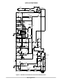
Figure 11. Schematic for the NCP1351 40 W Printer Evaluation Board
100 m
R
sense
V
CC
47 m
+
4.7 m
+
V
aux
1000 m
+
+
100 m
4.7 m
4.7 m
1000 m
+ +
100 m
DF05M
+
D1
Q1
NC
0
10 m
L1
C101NC
R17
NC
R12
0
1.5 m
2.7 k

NCP1351PRINTGEVB
http://onsemi.com
8
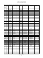
Table 4. BILL OF MATERIAL FOR THE NCP1351 40 W PRINTER EVALUATION BOARD
Designator Qty. Description Value Tolerance Footprint Manufacturer
Manufacturer
Part Number
Substitution
Allowed
Lead
Free
C1, C4,
C15, C18,
C21
5 SMD Capacitor 100 nF/50 V 5% SOD−1206 Vishay VJ1206Y104KXAA Yes Yes
C3 1 Electrolytic
Capacitor
4.7 mF/50 V
20% Radial −
OD 5 mm
Panasonic ECEA1HN100U Yes Yes
C6 1 SMD Capacitor 180 pF/50 V 5% SOD−1206 Vishay VJ1206A181KXAA Yes Yes
C7 1 Electrolytic
Capacitor
47 mF/50 V
20% Radial −
OD 5 mm
Panasonic ECA1HM470 Yes Yes
C8 1 SMD Capacitor 10 nF/50 V 5% SOD−1206 Vishay VJ1206Y103KXAA Yes Yes
C10 1 SMD Capacitor
1.5 mF
10% SOD−1206 Murata GRM31MR71C155K Yes Yes
C12 1 Film Capacitor 10 nF/630 V 5% Radial Epcos B32521N8103J Yes Yes
C13 1 Electrolytic
Capacitor
100 mF/400 V
20% Radial −
OD 20 mm
United chemicon EKXG401ELL101MMN3S Yes Yes
C14 1 X2 Capacitor 330 nF/250 Vac 20% Radial Epcos B32923A2334M Yes Yes
C16 1 Electrolytic
Capacitor
1,000 mF/50 V
20% Radial −
OD
12.5 mm
Panasonic ECA1HHG102 Yes Yes
C17 1 Electrolytic
Capacitor
100 mF/50 V
20% Radial −
OD 10 mm
Panasonic EEUEB1H101S Yes Yes
C19 1 Electrolytic
Capacitor
1,000 mF/25 V
20% Radial −
OD
12.5 mm
Panasonic ECA1EHG102 Yes Yes
C20 1 Electrolytic
Capacitor
100 mF/25 V
20% Radial −
OD 10 mm
Panasonic EEUEB1E101 Yes Yes
C23 1 Y1 Capacitor 2.2 nF/250 Vac 20% Radial TDK CD12−E2GA222MYNS Yes Yes
D1 1 SMD Resistor
0 W/0.25 W
5% SOD−1206 Vishay CRCW12060000Z0EA Yes Yes
D3 1 High-voltage
Switching
Diode
200 mA/200 V − SOT−23 ON Semiconductor BAS20LT1G No Yes
D4 1 Fast-recovery
Rectifier
1 A/600 V − Axial ON Semiconductor 1N4937G No Yes
D5, D7 2 Schottky
Rectifier
20 A/100 V − TO−220 ON Semiconductor MBR20100CTG No Yes
D9 1 Zener Diode 17 V/0.5 W 5% SOD−123 ON Semiconductor MMSZ5247BT1G No Yes
D10 1 Zener Diode 60 V/0.5 W 5% SOD−123 ON Semiconductor MMSZ5264BT1G No Yes
D11 1 Switching
Diode
200 mA/75 V − SOD−123 ON Semiconductor MMSD4148T1G No Yes
D12 1 Zener Diode 6.2 V/0.5 W 5% SOD−123 ON Semiconductor MMSZ5234BT1G No Yes
D13 1 Standard
Rectifier
1 A/1,000 V − Axial ON Semiconductor 1N4007G No Yes
HS1 1 Heatsink 13.4°C/W − Radial Aavid Thermalloy 531002B02500G Yes Yes
HS2, HS3 2 TO-220
Heatsink
24°C/W − − Aavid Thermalloy 577202B00000G Ye s Yes
U1 1 Rectifier Bridge 1 A/600 V − DIP−4 Micro Commercial Co. DB105-BP No Yes
U2 1 CMOS IC − − SOIC−8 ON Semiconductor NCP1351CDR2G No Yes
X4 1 Optocoupler − − DIP−4 CEL-NEC PS2501−1−H-A No Yes
X6 1 Common-mode
Choke
2 × 15 mH/1 A − Radial Panasonic ELF−25F108A No Yes
X10 1 Shunt
Regulator
2.5–36 V 5% TO−92 ON Semiconductor TL431CLPG No Yes
X11 1 Power
MOSFET
N-Channel
3 A/600 V − TO−220 Rohm 2SK2792 No Yes
T1 1 Transformer − − Radial Coilcraft GA0007−AL No Yes
J1 1 Connector 230 Vac − Radial Qualtek 771W−X2/02 Yes Yes
F1 1 Fuse 2 A/250 Vac T Radial Wickmann 37212000411 Yes Yes
L1 1 SMD Inductor
10 mH
− SMD Coilcraft DO1605T−ML No Yes
L2, L3 2 Inductor
4.7 mH/4.3 A
20% Radial API Delevan Inc. 4554−4R7M Yes Yes
R1 1 SMD Resistor
15 W/0.25 W
5% SOD−1206 Vishay CRCW120615R0JNEA Yes Yes

NCP1351PRINTGEVB
http://onsemi.com
9
Table 4. BILL OF MATERIAL FOR THE NCP1351 40 W PRINTER EVALUATION BOARD (continued)
Designator
Lead
Free
Substitution
Allowed
Manufacturer
Part Number
ManufacturerFootprintToleranceValueDescriptionQty.
R2 1 Resistor
4.7 MW/0.33 W
5% Axial − − Yes Yes
R5, R6 2 SMD Resistor
330kW/0.25 W
1% SOD−1206 Vishay CRCW1206330RFKEA Yes Yes
R7 1 SMD Resistor
0 W/0.25 W
5% SOD−1206 Vishay CRCW12060000Z0EA Yes Yes
R8, R19 2 SMD Resistor
2.7 kW/0.25 W
5% SOD−1206 Vishay CRCW12062R70JNEA Yes Yes
R9, R12 2 SMD Resistor
0 W/0.25 W
5% SOD−1206 Vishay CRCW12060000Z0EA Yes Yes
R10, R11,
R18
3 SMD Resistor
1kW/0.25 W
5% SOD−1206 Vishay CRCW12061K00JNEA Ye s Yes
R13 1 SMD Resistor
3.4 kW/0.25 W
1% SOD−1206 Vishay CRCW12063K40FKEA Yes Yes
R14 1 SMD Resistor
0.33 W/0.5 W
1% SOD−1206 − − Yes Yes
R15 1 Resistor
150 kW/2 W
5% Axial − − Yes Yes
R20 1 SMD Resistor
100 kW/0.25 W
1% SOD−1206 Vishay CRCW1206100KFKEA Yes Yes
R21 1 SMD Resistor
56 kW/0.25 W
1% SOD−1206 Vishay CRCW120656K0FKEA Yes Yes
R22 1 SMD Resistor
10 kW/0.25 W
1% SOD−1206 Vishay CRCW120610K0FKEA Yes Yes
R23, R24 2 SMD Resistor
3.3 MW/0.25 W
5% SOD−1206 Vishay CRCW12063M30JNEA Yes Yes
R26 1 SMD Resistor
0 W/0.25 W
1% SOD−1206 Vishay CRCW12060000FKEA Yes Yes
R28 1 SMD Resistor
8.2 kW/0.25 W
1% SOD−1206 Vishay CRCW12068K20FKEA Yes Yes
R30 1 SMD Resistor
47 kW/0.25 W
1% SOD−1206 Vishay CRCW120647K0FKEA Yes Yes
R31 1 SMD Resistor
180 kW/0.25 W
1% SOD−1206 Vishay CRCW1206180KFKEA Yes Yes
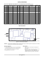
TEST PROCEDURE
Figure 12. Test Procedure Schematic
AC Input
(85−265 Vac)
16 V Output
0 V
32 V Output
WARNING: Be careful when manipulating the boards in operation, lethal voltages up to 600 V are present on the primary side. An isolation
transformer is also recommended for safer manipulations.
Necessary Equipment
• 1 current limited 230 Vrms AC source (current limited
to avoid board destruction in case of a defective part)
• 1 DC volt-meter able to measure up to 50 V DC
• 2 programmable electronic loads
Test Procedure
1. Apply 110 Vac on the Vin pins. Output pins are
left floating.
2. Measure the output voltage between pins +16 V et
GND and between +32 V and GND with a
volt-meter on the 50 V range. The measurements
should be respectively 16 and 32 volts (±10%).

NCP1351PRINTGEVB
http://onsemi.com
10
3. Connect an electronic load between pins +32 V
and GND, and set up a current of 1 A. Connect
another electronic load between pins +16 V and
GND, and set up a current of 0.625 A. Measure the
output voltages that should be respectively 16 and
32 volts (±10%).
4. Change the voltage applied on the Vin pins to
230 Vac. Measure the output voltages that should
again be respectively 16 and 32 volts (±10%).
5. Change the current setpoint for the electronic load
connected between pins +32 V and GND to 2.8 A.
The power supply should go to short-circuit
protection. Measure the output voltages that
should be 0 V.
6. Change the current setpoint for the electronic load
connected between pins +32 V and GND back to
1 A. Turn off the AC voltage source. Wait
5 seconds. Apply it again, the outputs should rise
again. Measure the output voltages that should
again be respectively 16 and 32 volts (±10%).
7. If every step has gone well, the board is
considered to be ok.
Microsoft Excel is a registered trademark of Microsoft Corporation.

www.onsemi.com
1
ON Semiconductor and the ON Semiconductor logo are trademarks of Semiconductor Components Industries, LLC dba ON Semiconductor or its subsidiaries in the United States and/or
other countries. ON Semiconductor owns the rights to a number of patents, trademarks, copyrights, trade secrets, and other intellectual property. A listing of ON Semiconductor’s
product/patent coverage may be accessed at www.onsemi.com/site/pdf/Patent−Marking.pdf
. ON Semiconductor is an Equal Opportunity/Affirmative Action Employer. This literature is
subject to all applicable copyright laws and is not for resale in any manner.
The evaluation board/kit (research and development board/kit) (hereinafter the “board”) is not a finished product and is as such not available for sale to consumers. The board is only intended
for research, development, demonstration and evaluation purposes and should as such only be used in laboratory/development areas by persons with an engineering/technical training
and familiar with the risks associated with handling electrical/mechanical components, systems and subsystems. This person assumes full responsibility/liability for proper and safe handling.
Any other use, resale or redistribution for any other purpose is strictly prohibited.
The board is delivered “AS IS” and without warranty of any kind including, but not limited to, that the board is production−worthy, that the functions contained in the board will meet your
requirements, or that the operation of the board will be uninterrupted or error free. ON Semiconductor expressly disclaims all warranties, express, implied or otherwise, including without
limitation, warranties of fitness for a particular purpose and non−infringement of intellectual property rights.
ON Semiconductor reserves the right to make changes without further notice to any board.
You are responsible for determining whether the board will be suitable for your intended use or application or will achieve your intended results. Prior to using or distributing any systems
that have been evaluated, designed or tested using the board, you agree to test and validate your design to confirm the functionality for your application. Any technical, applications or design
information or advice, quality characterization, reliability data or other services provided by ON Semiconductor shall not constitute any representation or warranty by ON Semiconductor,
and no additional obligations or liabilities shall arise from ON Semiconductor having provided such information or services.
The boards are not designed, intended, or authorized for use in life support systems, or any FDA Class 3 medical devices or medical devices with a similar or equivalent classification in
a foreign jurisdiction, or any devices intended for implantation in the human body. Should you purchase or use the board for any such unintended or unauthorized application, you shall
indemnify and hold ON Semiconductor and its officers, employees, subsidiaries, affiliates, and distributors harmless against all claims, costs, damages, and expenses, and reasonable
attorney fees arising out of, directly or indirectly, any claim of personal injury or death associated with such unintended or unauthorized use, even if such claim alleges that ON Semiconductor
was negligent regarding the design or manufacture of the board.
This evaluation board/kit does not fall within the scope of the European Union directives regarding electromagnetic compatibility, restricted substances (RoHS), recycling (WEEE), FCC,
CE or UL, and may not meet the technical requirements of these or other related directives.
FCC WARNING – This evaluation board/kit is intended for use for engineering development, demonstration, or evaluation purposes only and is not considered by ON Semiconductor to
be a finished end product fit for general consumer use. It may generate, use, or radiate radio frequency energy and has not been tested for compliance with the limits of computing devices
pursuant to part 15 of FCC rules, which are designed to provide reasonable protection against radio frequency interference. Operation of this equipment may cause interference with radio
communications, in which case the user shall be responsible, at its expense, to take whatever measures may be required to correct this interference.
ON Semiconductor does not convey any license under its patent rights nor the rights of others.
LIMITATIONS OF LIABILITY: ON Semiconductor shall not be liable for any special, consequential, incidental, indirect or punitive damages, including, but not limited to the costs of
requalification, delay, loss of profits or goodwill, arising out of or in connection with the board, even if ON Semiconductor is advised of the possibility of such damages. In no event shall
ON Semiconductor’s aggregate liability from any obligation arising out of or in connection with the board, under any theory of liability, exceed the purchase price paid for the board, if any.
For more information and documentation, please visit www.onsemi.com
.
PUBLICATION ORDERING INFORMATION
TECHNICAL SUPPORT
North American Technical Support:
Voice Mail: 1 800−282−9855 Toll Free USA/Canada
Phone: 011 421 33 790 2910
LITERATURE FULFILLMENT:
Email Requests to: [email protected]
ON Semiconductor Website: www.onsemi.com
Europe, Middle East and Africa Technical Support:
Phone: 00421 33 790 2910
For additional information, please contact your local Sales Representative
◊
-
 1
1
-
 2
2
-
 3
3
-
 4
4
-
 5
5
-
 6
6
-
 7
7
-
 8
8
-
 9
9
-
 10
10
-
 11
11


ON Semiconductor NCP1351 Series User manual
- Type
- User manual
- This manual is also suitable for
Ask a question and I''ll find the answer in the document
Finding information in a document is now easier with AI
Related papers
-
ON Semiconductor 25VT6A5VGEVB User manual
-
-
ON Semiconductor RSL10 Getting Started Manual
-
-
-
-
-
-
Other documents
-
 onsemi NCL31000ASGEVB LED Driver Evaluation Board User guide
-
Texas Instruments LM3444 Evaluation Boards LM3444-230VFLBK/NOPB Datasheet
-
Microchip Technology HV9805 User manual
-
-
-
NXP TEA175X User guide
-
NXP TEA173X User guide
-
-
-
Analog Devices ADP1071-1EVALZ User manual
