
UM10772
User Manual BFU5xx series starter kits
Rev. 1 — 21 January 2014
User manual
Document information
Info
Content
Keywords
BFU520, BFU530, BFU550, BFU520A, BFU530A, BFU550A, BFU520W
BFU530W, BFU550W, BFU520X, BFU530X, BFU550X, BFU520XR,
BFU530XR, BFU550XR, amplifier, LNA, Wide Band Amplifier, PCB
layout, Assembly drawings
Abstract
Document that describes the PCB’s and SW content as delivered in the
BFU5xx series transistor starter kit

NXP Semiconductors
UM10772
How to use BFU5xx starter-kit
UM10772
© NXP B.V. 2014. All rights reserved.
User manual
Rev. 1 — 21 January 2014
2 of 29
Contact information
For additional information, please visit:
http://www.nxp.com
For sales office addresses, please send an email to: salesaddresses@nxp.com
Revision history
Rev
Date
Description
1
2014-01-21
First publication

NXP Semiconductors
UM10772
How to use BFU5xx starter-kit
UM10772
All information provided in this document is subject to legal disclaimers.
© NXP B.V. 2014. All rights reserved.
User manual
Rev. 1 — 21 January 2014
3 of 29
1. Introduction
The BFU5xxX transistor family is designed to meet the latest requirements on high frequency
applications (up to approximately 1.5 GHz) such as communication, automotive and industrial
equipment.
As soon as fast, low noise analogue signal processing is required, combined with medium to high
voltage swings, the BFU5xxX transistors are the perfect choice. Due to the high gain at low supply
current those types can also be applied very well in battery fed equipment.
Compared to previous Philips / NXP transistor generations and competitor products, improvements
on gain, noise and thermal properties are realized. BFU5xxX transistors will be available in various
packages.
The transistors will be promoted with a full promotion package, called “starter kits” (one kit type per
package-type). Those kits include two PCB’s (one with grounded emitter, one with emitter
degeneration provision), RF connectors, transistors and simulation model parameters required to
perform simulations. See the overview of available starter kits in the table below.
Table 1. Customer evaluation kits
Transistor Types
Evaluation Kit
BFU520, BFU530, BFU550
OM7962, starter kit SOT143
BFU520X, BFU530X, BFU550X
OM7963, starter kit SOT143X
BFU520XR, BFU530XR, BFU550XR
OM7964, starter kit SOT143XR
BFU520A, BFU530A, BFU550A
OM7961, starter kit SOT23
BFU520W, BFU530W, BFU550W
OM7960, starter kit SOT323

NXP Semiconductors
UM10772
How to use BFU5xx starter-kit
UM10772
All information provided in this document is subject to legal disclaimers.
© NXP B.V. 2014. All rights reserved.
User manual
Rev. 1 — 21 January 2014
4 of 29
Table 2. Application Notes
Transistor Type
Application Notes (433MHz LNA; 866MHz LNA)
BFU520
AN11427; AN11428
BFU530
AN11429; AN11430
BFU550
AN11431; AN11432
BFU520A
AN11377; AN11378
BFU530A
AN11379; AN11380
BFU550A
AN11381; AN11382
BFU520W
AN11421; AN11422
BFU530W
AN11423; AN11424
BFU550W
AN11425; AN11426
BFU520X
AN11433; AN11434
BFU530X
AN11435; AN11436
BFU550X
AN11437; AN11438
BFU520XR
AN11439; AN11440
BFU530XR
AN11441; AN11442
BFU550XR
AN11443; AN11444
2. Content of the starter kits
The starter kits contains following items:
1) 10 transistors of BFU520W
2) 10 transistors of BFU530W
3) 10 transistors of BFU550W
4) One generic Printed Circuit Board for amplifier design with grounded emitter
5) One generic Printed Circuit Board for amplifier design using feedback via emitter
6) 4 SMA connectors
7) 2 DC connectors
8) A USB memory stick containing Application notes, models, datasheets, S parameter data

NXP Semiconductors
UM10772
How to use BFU5xx starter-kit
UM10772
All information provided in this document is subject to legal disclaimers.
© NXP B.V. 2014. All rights reserved.
User manual
Rev. 1 — 21 January 2014
5 of 29
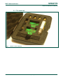
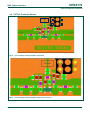
2.1 The starter kit
Fig 1. BFU5xx series starter kit

NXP Semiconductors
UM10772
How to use BFU5xx starter-kit
UM10772
All information provided in this document is subject to legal disclaimers.
© NXP B.V. 2014. All rights reserved.
User manual
Rev. 1 — 21 January 2014
6 of 29
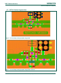
2.2 PCB’s example for BFU5xx series LNA
Fig 2. PCB’s BFU5-- series populated board, example 433MHz LNA in SOT143 package
3. Target applications for starter kit PCB’s
Basically the PCB’s are designed to accommodate an RF amplifier. These could be:
1) LNA’s
2) Generic RF Amplifiers, small signal, small band
3) Wide band amplifiers (by applying feedback)
4) Amplifiers for large signal (using for example BFU550 types).

NXP Semiconductors
UM10772
How to use BFU5xx starter-kit
UM10772
All information provided in this document is subject to legal disclaimers.
© NXP B.V. 2014. All rights reserved.
User manual
Rev. 1 — 21 January 2014
7 of 29
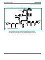
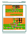
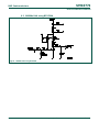
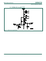
3.1 Basic schematic for Grounded Emitter versions (VGE0x)
Fig 3. Schematic Amplifier design VGE
Remarks:
- Not all components are required, depends on amplifier/matching configuration
- Input and output considered to be 50 Ohms characteristic impedance (SMA type)
- Generic PI or T matching network at input and output possible
- Basically on all BFU5xx series amplifier EVB’s this schematic is applied, small variations on
implementation are possible
Zin2
TR1
Zin1
Zin5
Zin3
Zin6
RF input
Zc1 Zc2
C4
C5
Zc3
Zbias2Zbias1
Zfb2
Zfb1
Zout1
Zout4
Zout2
Zout5
Zout3
Celectrolytic +
RF output
Zin4
Zbias3
C7
C3
C2
C1
C6
Zfb3

NXP Semiconductors
UM10772
How to use BFU5xx starter-kit
UM10772
All information provided in this document is subject to legal disclaimers.
© NXP B.V. 2014. All rights reserved.
User manual
Rev. 1 — 21 January 2014
8 of 29
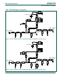
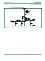
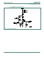
3.2 Basic schematic for Emitter Degeneration version (VED0x)
Fig 4. Schematic Amplifier design VED
Remarks:
- Not all components are required, depends on amplifier/matching configuration
- Input and output considered to be 50 Ohms characteristic impedance (SMA type)
- Two parallel components from emitter to GND enable to split DC/AC
- Generic PI or T matching network at input and output possible
Basically on all BFU5xx series amplifier EVB’s this schematic is applied, small variations on
implementation are possible
Zin2
TR1
Zin1
Zin5
Zin3
Zin6
RF input
Zc1
Zc2
C4
C5
Zc3
Zbias2Zbias1
Zfb2
Zfb1
Zout1
Zout4
Zout2
Zout5
Zout3
Celectrolytic +
RF output
Zin4
Zbias3
C7
C3
C2
C1
C6
Zfb3
Ze1
Ze2

NXP Semiconductors
UM10772
How to use BFU5xx starter-kit
UM10772
All information provided in this document is subject to legal disclaimers.
© NXP B.V. 2014. All rights reserved.
User manual
Rev. 1 — 21 January 2014
9 of 29
4. PCB drawings for all versions
On all PCB’s, except SOT143XR types the same circuit can be applied. On all PCB’s
except the SOT323, 0603 footprints for capacitors/inductors/resistors are implemented.
For SOT323 types this is reduced to 0402 because of the smaller size transistor
package.
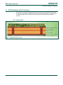
4.1 Layer stack
Fig 5. Applied PCB layout stack

NXP Semiconductors
UM10772
How to use BFU5xx starter-kit
UM10772
All information provided in this document is subject to legal disclaimers.
© NXP B.V. 2014. All rights reserved.
User manual
Rev. 1 — 21 January 2014
10 of 29
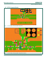
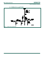
4.2 SOT323 Grounded Emitter
Fig 6. PCB Assembly drawing Amplifier design VGE
Fig 7. PCB Assembly drawing Amplifier design VGE zoomed in
Zin1 Zin2
Zin3
Zin4
Zin5
Zfb1
Zfb2
Zout1 Zout2
Zout3
Zout4
Zout5
Zb1
Zb2
Zc1 Zc2
C1
C2
C3
C4
C6
Celectrolytic
RF input SMA
RF output SMA
+Vcc
GND
TR1
+
Zc3
GND
C5
Zin6
Zfb3
C7
Zb3

NXP Semiconductors
UM10772
How to use BFU5xx starter-kit
UM10772
All information provided in this document is subject to legal disclaimers.
© NXP B.V. 2014. All rights reserved.
User manual
Rev. 1 — 21 January 2014
11 of 29
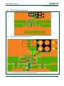
4.3 SOT323 Emitter Degeneration
Fig 8. PCB Assembly drawing Amplifier design VED
Fig 9. PCB Assembly drawing Amplifier design VED zoomed in
Zin1
Zin2
Zin3
Zin4
Zin5
Zfb1
Zfb2
Zout1 Zout2 Zout3
Zout4
Zout5
Zb1
Zb2
Zc1
Zc2
C1
C2
C3
C4
C6
Celectrolytic
RF input SMA
RF output SMA
+Vcc
GND
TR1
+
Zc3
GND
C5
Zin6
Zfb3
C7
Zb3
Ze1
Ze2

NXP Semiconductors
UM10772
How to use BFU5xx starter-kit
UM10772
All information provided in this document is subject to legal disclaimers.
© NXP B.V. 2014. All rights reserved.
User manual
Rev. 1 — 21 January 2014
12 of 29
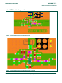
4.4 SOT23 Grounded Emitter
Fig 10. PCB Assembly drawing Amplifier design VGE
Fig 11. PCB Assembly drawing Amplifier design VGE zoomed in
Zin1
Zin2
Zin3
Zin4
Zin5
RF input SMA
RF output SMA
Zfb1
Zfb2
Zout1
Zout2
Zout3
Zout4
Zout5
Zc1
TR1
Zbias1
Zbias2
C3C4
C5
C1
C2
Celectrolytic
+Vcc
Supply
GND
Zfb3
Zin6
Zc2
Zc3
Zbias3

NXP Semiconductors
UM10772
How to use BFU5xx starter-kit
UM10772
All information provided in this document is subject to legal disclaimers.
© NXP B.V. 2014. All rights reserved.
User manual
Rev. 1 — 21 January 2014
13 of 29
4.5 SOT23 Emitter Degeneration
Fig 12. PCB Assembly drawing Amplifier design VED
Fig 13. PCB Assembly drawing Amplifier design VED zoomed in
Zin1
Zin2
Zin3
Zin4
Zin5
RF input SMA
Zfb1
Zfb2
Zout1 Zout2
Zout3
Zout4
Zout5
Zc1
TR1
Zbias1
Zbias2
C3C4
C5
C1
C2
Celectrolytic
+Vcc
Supply
GND
Zfb3
Zin6
Zc2
Zc3
Zbias3
Ze1
Ze2
RF output SMA

NXP Semiconductors
UM10772
How to use BFU5xx starter-kit
UM10772
All information provided in this document is subject to legal disclaimers.
© NXP B.V. 2014. All rights reserved.
User manual
Rev. 1 — 21 January 2014
14 of 29
4.6 SOT143 Grounded Emitter
Fig 14. PCB Assembly drawing Amplifier design VGE
Fig 15. PCB Assembly drawing Amplifier design VGE zoomed in
Zin1 Zin2 Zin3
Zin4
Zin5
Zfb1
Zfb2
Zout1
Zout2 Zout3
Zout4
Zout5
Zc1
TR1
Zbias1
C3
C4
C7
C1
C2
Celectrolytic
+Vcc
Supply
GND
Zin6
Zc2
Zc3
Zfb3
Zbias2Zbias3
RF input SMA RF output SMA

NXP Semiconductors
UM10772
How to use BFU5xx starter-kit
UM10772
All information provided in this document is subject to legal disclaimers.
© NXP B.V. 2014. All rights reserved.
User manual
Rev. 1 — 21 January 2014
15 of 29
4.7 SOT143 Emitter Degeneration
Fig 16. PCB Assembly drawing Amplifier design VED
Fig 17. PCB Assembly drawing Amplifier design VED zoomed in
Zin1 Zin2 Zin3
Zin4
Zin5
Ze2
Zfb2
Zout1
Zout2 Zout3
Zout4
Zout5
Zc1
TR1
Zbias1
C3
C4
C7
C1
C2
Celectrolytic
+Vcc
Supply
GND
Zin6
Zc2
Zc3
Zfb3
Zbias2Zbias3
RF input SMA RF output SMA
Ze1
Zfb1

NXP Semiconductors
UM10772
How to use BFU5xx starter-kit
UM10772
All information provided in this document is subject to legal disclaimers.
© NXP B.V. 2014. All rights reserved.
User manual
Rev. 1 — 21 January 2014
16 of 29
4.8 SOT143X Grounded Emitter
Fig 18. PCB Assembly drawing Amplifier design VGE
Fig 19. PCB Assembly drawing Amplifier design VGE zoomed in
Zin1 Zin2
Zin3
Zin4
Zin5
Zfb1
Zfb2
Zout1
Zout2
Zout3
Zout4
Zout5
Zc1
TR1
Zbias1
C3
C4
C7
C1
C2
Celectrolytic
+Vcc
Supply
GND
Zin6
Zc2
Zc3
Zfb3
Zbias2
Zbias3
RF input SMA RF output SMA

NXP Semiconductors
UM10772
How to use BFU5xx starter-kit
UM10772
All information provided in this document is subject to legal disclaimers.
© NXP B.V. 2014. All rights reserved.
User manual
Rev. 1 — 21 January 2014
17 of 29
4.9 SOT143X Emitter Degeneration
Fig 20. PCB Assembly drawing Amplifier design VED
Fig 21. PCB Assembly drawing Amplifier design VED zoomed in
Zin1 Zin2
Zin3
Zin4
Zin5
Zfb1
Zfb2
Zout1
Zout2
Zout3
Zout4
Zout5
Zc1
TR1
Zbias1
C3
C4
C7
C1
C2
Celectrolytic
+Vcc
Supply
GND
Zin6
Zc2
Zc3
Zfb3
Zbias2
Zbias3
RF input SMA RF output SMA
Ze1
Ze2

NXP Semiconductors
UM10772
How to use BFU5xx starter-kit
UM10772
All information provided in this document is subject to legal disclaimers.
© NXP B.V. 2014. All rights reserved.
User manual
Rev. 1 — 21 January 2014
18 of 29
4.10 SOT143XR types, schematics
Fig 22. Generic schematic used for SOT143XR Vge types, small differences in DC biasing
Fig 23. Generic schematic used for SOT143XR Ved types, small differences in DC biasing
Zin2
TR1
Zin1
Zin5
Zin3
Zbias2
RF input
Zc1
Zc2
C4
C5
Zc3
Zfb2
Zfb1
Zout1
Zout4
Zout2
Zout5
Zout3
Celectrolytic +
RF output
Zin4
Zbias1
C7
C3
C2
C1
C6
Zfb3
Zin2
TR1
Zin1
Zin5
Zin3
Zbias2
RF input
Zc1 Zc2
C4
C5
Zc3
Zfb2
Zfb1
Zout1
Zout4
Zout2
Zout5
Zout3
Celectrolytic +
RF output
Zin4
Zbias1
C7
C3
C2
C1
C6
Zfb3
Ze1
Ze2

NXP Semiconductors
UM10772
How to use BFU5xx starter-kit
UM10772
All information provided in this document is subject to legal disclaimers.
© NXP B.V. 2014. All rights reserved.
User manual
Rev. 1 — 21 January 2014
19 of 29
4.11 SOT143XR Grounded Emitter
Fig 24. PCB Assembly drawing Amplifier design VGE
Fig 25. PCB Assembly drawing Amplifier design VGE zoomed in
Zin1 Zin2
Zin3
Zin4
Zin5
Zfb1
Zfb2
Zout1 Zout2
Zout3
Zout4
Zout5
Zc1
TR1
Zbias1
C3
C4
C1
C2
Celectrolytic
+Vcc
Supply
GND
Zc2
Zc3
Zfb3
Zbias2
RF input SMA RF output SMA
C6
C7

NXP Semiconductors
UM10772
How to use BFU5xx starter-kit
UM10772
All information provided in this document is subject to legal disclaimers.
© NXP B.V. 2014. All rights reserved.
User manual
Rev. 1 — 21 January 2014
20 of 29
4.12 SOT143XR Emitter Degeneration
Fig 26. PCB Assembly drawing Amplifier design VED
Fig 27. PCB Assembly drawing Amplifier design VED zoomed in
Zin1 Zin2
Zin3
Zin4
Zin5
Zfb1
Zfb2
Zout1 Zout2
Zout3
Zout4
Zout5
Zc1
TR1
Zbias1
C3
C4
C1
C2
Celectrolytic
+Vcc
Supply
GND
Zc2
Zc3
Zfb3
Zbias2
RF input SMA RF output SMA
C6
C7
Ze1
Ze2
Page is loading ...
Page is loading ...
Page is loading ...
Page is loading ...
Page is loading ...
Page is loading ...
Page is loading ...
Page is loading ...
Page is loading ...
-
 1
1
-
 2
2
-
 3
3
-
 4
4
-
 5
5
-
 6
6
-
 7
7
-
 8
8
-
 9
9
-
 10
10
-
 11
11
-
 12
12
-
 13
13
-
 14
14
-
 15
15
-
 16
16
-
 17
17
-
 18
18
-
 19
19
-
 20
20
-
 21
21
-
 22
22
-
 23
23
-
 24
24
-
 25
25
-
 26
26
-
 27
27
-
 28
28
-
 29
29


