Page is loading ...

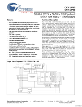
10 Gb/s 3.3V QuadPort™ DSE Family
CY7C0430BV
CY7C0430CV
Cypress Semiconductor Corporation • 198 Champion Court • San Jose, CA 95134-1709 • 408-943-2600
Document #: 38-06027 Rev. *B Revised May 23, 2006
Features
• QuadPort™ datapath switching element (DSE) family
allows four independent ports of access for data path
management and switching
• High-bandwidth data throughput up to 10 Gb/s
• 133-MHz
[1]
port speed x 18-bit-wide interface × 4 ports
• High-speed clock to data access 4.2 ns (max.)
• Synchronous pipelined device
— 1-Mb (64K × 18) switch array
• 0.25-micron CMOS for optimum speed/power
• IEEE 1149.1 JTAG boundary scan
• Width and depth expansion capabilities
• BIST (Built-In Self-Test) controller
• Dual Chip Enables on all ports for easy depth expansion
• Separate upper-byte and lower-byte controls on all
ports
• Simple array partitioning
— Internal mask register controls counter wrap-around
— Counter-Interrupt flags to indicate wrap-around
— Counter and mask registers readback on address
• 272-ball BGA package (27-mm × 27-mm × 1.27-mm ball
pitch)
• Commercial and industrial temperature ranges
• 3.3V low operating power
— Active = 750 mA (maximum)
— Standby = 15 mA (maximum
Note:
1. f
MAX2
for commercial is 135 MHz and for industrial is 133 MHz.
BUFFERED SWITCH
REDUNDANT DATA MIRROR
PORT 1 PORT 3
PORT 4
PORT 2
PORT 1
PORT 2
PORT 3
PORT 4
QuadPort DSE Family Applications
[+] Feedback

CY7C0430BV
CY7C0430CV
Document #: 38-06027 Rev. *B Page 2 of 37
Functional Description
The Quadport Datapath Switching Element (DSE) family offers
four ports that may be clocked at independent frequencies
from one another. Each port can read or write up to 133 MHz
[1]
,
giving the device up to 10 Gb/s of data throughput. The device
is 1-Mb (64K × 18) in density. Simultaneous reads are allowed
for accesses to the same address location; however, simulta-
neous reading and writing to the same address is not allowed.
Any port can write to a certain location while other ports are
reading that location simultaneously, if the timing spec for port
to port delay (t
CCS
) is met. The result of writing to the same
location by more than one port at the same time is undefined.
Data is registered for decreased cycle time. Clock to data valid
t
CD2
= 4.2 ns. Each port contains a burst counter on the input
address register. After externally loading the counter with the
initial address the counter will self-increment the address inter-
nally (more details to follow). The internal write pulse width is
independent of the duration of the R/W
input signal. The
internal write pulse is self-timed to allow the shortest possible
cycle times.
A HIGH on CE
0
or LOW on CE
1
for one clock cycle will power
down the internal circuitry to reduce the static power
consumption. One cycle is required with chip enables asserted
to reactivate the outputs.
The CY7C0430BV and CY7C0430CV (64K × 18 device)
supports burst contains for simple array partitioning. Counter
enable inputs are provided to stall the operation of the address
input and utilize the internal address generated by the internal
counter for fast interleaved memory applications. A port’s burst
DATA PATH AGGREGATOR
PORT 1
PORT 2
PORT 3
PORT 4
DATA PATH MANAGER FOR
PARALLEL PACKET PROCESSING
Processor 2
Processor 1
Pre-processed DATA Path Processed DATA Path
DATA CLASSIFICATION ENGINE
PORT 2 PORT 4
PORT 1 PORT 3
Queue #1
Queue #2
QuadPort
DSE Family
[+] Feedback

CY7C0430BV
CY7C0430CV
Document #: 38-06027 Rev. *B Page 3 of 37
counter is loaded with an external address when the port’s
Counter Load pin (CNTLD
) is asserted LOW. When the port’s
Counter Increment pin (CNTINC
) is asserted, the address
counter will increment on each subsequent LOW-to- HIGH
transition of that port’s clock signal. This will read/write one
word from/into each successive address location until
CNTINC
is deasserted. The counter can address the entire
switch array and will loop back to the start. Counter Reset
(CNTRST) is used to reset the burst counter. A counter-mask
register is used to control the counter wrap. The counter and
mask register operations are described in more details in the
following sections.
The counter or mask register values can be read back on the
bidirectional address lines by activating MKRD
or CNTRD,
respectively.
The new features included for the QuadPort DSE family
include: readback of burst-counter internal address value on
address lines, counter-mask registers to control the counter
wrap-around, readback of mask register value on address
lines, interrupt flags for message passing, BIST, JTAG for
boundary scan, and asynchronous Master Reset.
Notes:
2. Port 1 Control Logic Block is detailed on page 4.
3. Port 2, Port 3, and Port 4 Logic Blocks are similar to Port 1 Logic Blocks.
Port-1
Control
Logic
Port 1
Counter/
Mask Reg/
Address
Decode
Port 1
I/O
18
Top Level Logic Block Diagram
64K × 18
QuadPort DSE
Array
Port 1 Operation-control Logic Blocks
[2]
Port 2 Logic Blocks
[3]
Port 4 Logic Blocks
[3]
Port 3 Logic Blocks
[3]
CNTLD
P1
CNTINC
P1
CNTRST
P1
MKLD
P1
CNTINT
P1
MKRD
P1
CNTRD
P1
INT
P1
CE
1P1
CE
0P1
R/W
P1
OE
P1
UB
P1
LB
P1
I/O
0P1
- I/O
17P1
A
0P1
–A
15P1
16
TMS
TCK
TDI
TDO
BIST
MRST
Reset
Logic
JTAG
Controller
CLK
P1
CLK
P1
CLKBIST
Port 1
Port 2
Port 3
Port 4
[+] Feedback

CY7C0430BV
CY7C0430CV
Document #: 38-06027 Rev. *B Page 4 of 37
Addr.
Read
Port 1 Operation-Control Logic Block Diagram
R/W
P1
CE
0P1
CE
1P1
LB
P1
OE
P1
UB
P1
I/O
9P1
–I/O
17P1
I/O
0P1
–I/O
8P1
I/O
Control
Counter/
A
0P1
–A
15P1
CLK
P1
CNTLD
P1
CNTINC
P1
CNTRST
P1
16
9
9
MKLD
P1
CNTINT
P1
MKRD
P1
Mask Register
Port-1
Port 1
Port 1
64K × 18
QuadPort
DSE Array
P
or
t
1
Po
r
t 2
P
ort 4
P
ort 3
Address
Register
Readback
Register
Port 1
CNTRD
P1
Port 1
Address
Decode
Port 1
Interrupt
Logic
R/W
P1
CE
0P1
CE
1P1
OE
P1
INT
P1
CLK
P1
MRST
MRST
Priority
Decision
Logic
MRST
(Address Readback is independent of CEs)
W
LB
P1
UB
P1
[+] Feedback

CY7C0430BV
CY7C0430CV
Document #: 38-06027 Rev. *B Page 5 of 37
Pin Configuration
272-ball Grid Array (BGA)
Top View
Note:
4. Central Leads are for thermal dissipation only. They are connected to device V
SS
.
1234567891011121314151617181920
A
LB
P1
I/O17
P2
I/O15
P2
I/O13
P2
I/O11
P2
I/O9
P2
I/O16
P1
I/O14
P1
I/O12
P1
I/O10
P1
I/O10
P4
I/O12
P4
I/O14
P4
I/O16
P4
I/O9
P3
I/O11
P3
I/O13
P3
I/O15
P3
I/O17
P3
LB
P4
B
VDD1 UB
P1
I/O16
P2
I/O14
P2
I/O12
P2
I/O10
P2
I/O17
P1
I/O13
P1
I/O11
P1
TMS TDI I/O11
P4
I/O13
P4
I/O17
P4
I/O10
P3
I/O12
P3
I/O14
P3
I/O16
P3
UB
P4
VDD1
C
A14
P1
A15
P1
CE1
P1
CE0
P1
R/W
P1
I/O15
P1
VSS2 VSS2 I/O9
P1
TCK TDO I/O9
P4
VSS2 VSS2 I/O15
P4
R/W
P4
CE0
P4
CE1
P4
A15
P4
A14
P4
D
VSS1 A12
P1
A13
P1
OE
P1
VDD2 VSS2 VSS2 VDD2 VDD VSS VSS VDD VDD2 VSS2 VSS2 VDD2 OE
P4
A13
P4
A12
P4
VSS1
E
A10
P1
A11
P1
MKRD
P1
CNTRD
P1
CNTRD
P4
MKRD
P4
A11
P4
A10
P4
F
A7
P1
A8
P1
A9
P1
CNTINT
P1
CNTINT
P4
A9
P4
A8
P4
A7
P4
G
VSS1 A5
P1
A6
P1
CNTINC
P1
CNTINC
P4
A6
P4
A5
P4
VSS1
H
A3
P1
A4
P1
MKLD
P1
CNTLD
P1
CNTLD
P4
MKLD
P4
A4
P4
A3
P4
J
VDD1 A1
P1
A2
P1
VDD GND
[4]
GND
[4]
GND
[4]
GND
[4]
VDD A2
P4
A1
P4
VDD1
K
A0
P1
INT
P1
CNTRST
P1
CLK
P1
GND
[4]
GND
[4]
GND
[4]
GND
[4]
CLK
P4
CNTRST
P4
INT
P4
A0
P4
L
A0
P2
INT
P2
CNTRST
P2
VSS GND
[4]
GND
[4]
GND
[4]
GND
[4]
VSS CNTRST
P3
INT
P3
A0
P3
M
VDD1 A1
P2
A2
P2
CLK
P2
GND
[4]
GND
[4]
GND
[4]
GND
[4]
CLK
P3
A2
P3
A1
P3
VDD1
N
A3
P2
A4
P2
MKLD
P2
CNTLD
P2
CNTLD
P3
MKLD
P3
A4
P3
A3
P3
P
VSS1 A5
P2
A6
P2
CNTINC
P2
CNTINC
P3
A6
P3
A5
P3
VSS1
R
A7
P2
A8
P2
A9
P2
CNTINT
P2
CNTINT
P3
A9
P3
A8
P3
A7
P3
T
A10
P2
A11
P2
MKRD
P2
CNTRD
P2
CNTRD
P3
MKRD
P3
A11
P3
A10
P3
U
VSS1 A12
P2
A13
P2
OE
P2
VDD2 VSS2 VSS2 VDD2 VDD VSS VSS VDD VDD2 VSS2 VSS2 VDD2 OE
P3
A13
P3
A12
P3
VSS1
V
A14
P2
A15
P2
CE1
P2
CE0
P2
R/W
P2
I/O6
P2
VSS2 VSS2 I/O0
P2
NC NC I/O0
P3
VSS2 VSS2 I/O6
P3
R/W
P3
CE0
P3
CE1
P3
A15
P3
A14
P3
W
VDD1 UB
P2
I/O7
P1
I/O5
P1
I/O3
P1
I/O1
P1
I/O8
P2
I/O4
P2
I/O2
P2
MRST
CLKBIST I/O2
P3
I/O4
P3
I/O8
P3
I/O1
P4
I/O3
P4
I/O5
P4
I/O7
P4
UB
P3
VDD1
Y
LB
P2
I/O8
P1
I/O6
P1
I/O4
P1
I/O2
P1
I/O0
P1
1/O7
P2
I/O5
P2
I/O3
P2
I/O1
P2
I/O1
P3
I/O3
P3
I/O5
P3
I/O7
P3
I/O0
P4
I/O2
P4
I/O4
P4
I/O6
P4
I/O8
P4
LB
P3
[+] Feedback

CY7C0430BV
CY7C0430CV
Document #: 38-06027 Rev. *B Page 6 of 37
Selection Guide
CY7C0430CV
–133
CY7C0430CV
–100 Unit
f
MAX2
133
[1]
100 MHz
Max Access Time (Clock to Data) 4.2 5.0 ns
Max Operating Current I
CC
750 600 mA
Max Standby Current for I
SB1
(All ports TTL Level) 200 150 mA
Max Standby Current for I
SB3
(All ports CMOS Level) 15 15 mA
Pin Definitions
Port 1 Port 2 Port 3 Port 4 Description
A
0P1
–A
15P1
A
0P2
–A
15P2
A
0P3
–A
15P3
A
0P4
–A
15P4
Address Input/Output.
I/O
0P1
–I/O
17P1
I/O
0P2
–I/O
17P2
I/O
0P3
–I/O
17P3
I/O
0P4
–I/O
17P4
Data Bus Input/Output.
CLK
P1
CLK
P2
CLK
P3
CLK
P4
Clock Input. This input can be free running or strobed.
Maximum clock input rate is f
MAX
.
LB
P1
LB
P2
LB
P3
LB
P4
Lower Byte Select Input. Asserting this signal LOW
enables read and write operations to the lower byte. For
read operations both the LB and OE signals must be
asserted to drive output data on the lower byte of the data
pins.
UB
P1
UB
P2
UB
P3
UB
P4
Upper Byte Select Input. Same function as LB, but to the
upper byte.
CE
0P1
,CE
1P1
CE
0P2
,CE
1P2
CE
0P3
,CE
1P3
CE
0P4
,CE
1P4
Chip Enable Input. To select any port, both CE
0
AND
CE
1
must be asserted to their active states (CE
0
≤ V
IL
and
CE
1
≥ V
IH
).
OE
P1
OE
P2
OE
P3
OE
P4
Output Enable Input. This signal must be asserted LOW
to enable the I/O data lines during read operations. OE
is
asynchronous input.
R/W
P1
R/W
P2
R/W
P3
R/W
P4
Read/Write Enable Input. This signal is asserted LOW
to write to the dual port memory array. For read opera-
tions, assert this pin HIGH.
MRST Master Reset Input. This is one signal for All Ports.
MRST
is an asynchronous input. Asserting MRST LOW
performs all of the reset functions as described in the text.
A MRST
operation is required at power-up.
CNTRST
P1
CNTRST
P2
CNTRST
P3
CNTRST
P4
Counter Reset Input. Asserting this signal LOW resets
the burst address counter of its respective port to zero.
CNTRST
is second to MRST in priority with respect to
counter and mask register operations.
MKLD
P1
MKLD
P2
MKLD
P3
MKLD
P4
Mask Register Load Input. Asserting this signal LOW
loads the mask register with the external address
available on the address lines. MKLD
operation has
higher priority over CNTLD
operation.
CNTLD
P1
CNTLD
P2
CNTLD
P3
CNTLD
P4
Counter Load Input. Asserting this signal LOW loads the
burst counter with the external address present on the
address pins.
CNTINC
P1
CNTINC
P2
CNTINC
P3
CNTINC
P4
Counter Increment Input. Asserting this signal LOW
increments the burst address counter of its respective port
on each rising edge of CLK.
[+] Feedback

CY7C0430BV
CY7C0430CV
Document #: 38-06027 Rev. *B Page 7 of 37
CNTRD
P1
CNTRD
P2
CNTRD
P3
CNTRD
P4
Counter Readback Input. When asserted LOW, the
internal address value of the counter will be read back on
the address lines. During CNTRD
operation, both CNTLD
and CNTINC
must be HIGH. Counter readback operation
has higher priority over mask register readback operation.
Counter readback operation is independent of port chip
enables. If address readback operation occurs with chip
enables active (CE
0
= LOW, CE
1
= HIGH), the data lines
(I/Os) will be three-stated. The readback timing will be
valid after one no-operation cycle plus t
CD2
from the rising
edge of the next cycle.
MKRD
P1
MKRD
P2
MKRD
P3
MKRD
P4
Mask Register Readback Input. When asserted LOW,
the value of the mask register will be readback on address
lines. During mask register readback operation, all
counter and MKLD
inputs must be HIGH (see Counter
and Mask Register Operations truth table). Mask register
readback operation is independent of port chip enables.
If address readback operation occurs with chip enables
active (CE
0
= LOW, CE
1
= HIGH), the data lines (I/Os) will
be three-stated. The readback will be valid after one
no-operation cycle plus t
CD2
from the rising edge of the
next cycle.
CNTINT
P1
CNTINT
P2
CNTINT
P3
CNTINT
P4
Counter Interrupt Flag Output. Flag is asserted LOW
for one clock cycle when the counter wraps around to
location zero.
INTP1 INTP2 INTP3 INTP4 Interrupt Flag Output. Interrupt permits communications
between all four ports. The upper four memory locations
can be used for message passing. Example of operation:
INT
P4
is asserted LOW when another port writes to the
mailbox location of Port 4. Flag is cleared when Port 4
reads the contents of its mailbox. The same operation is
applicable to ports 1, 2, and 3.
TMS JTAG Test Mode Select Input. It controls the advance of
JTAG TAP state machine. State machine transitions occur
on the rising edge of TCK.
TCK JTAG Test Clock Input. This can be CLK of any port or
an external clock connected to the JTAG TAP.
TDI JTAG Test Data Input. This is the only data input. TDI
inputs will shift data serially in to the selected register.
TDO JTAG Test Data Output. This is the only data output.
TDO transitions occur on the falling edge of TCK. TDO
normally three-stated except when captured data is
shifted out of the JTAG TAP.
CLKBIST BIST Clock Input.
GND Thermal Ground for Heat Dissipation.
V
SS
Ground Input.
V
DD
Power Input.
V
SS1
Address Lines Ground Input.
V
DD1
Address Lines Power Input.
V
SS2
Data Lines Ground Input.
V
DD2
Data Lines Power Input.
Pin Definitions (continued)
Port 1 Port 2 Port 3 Port 4 Description
[+] Feedback

CY7C0430BV
CY7C0430CV
Document #: 38-06027 Rev. *B Page 8 of 37
Maximum Ratings
(Above which the useful life may be impaired. For user guide-
lines, not tested.)
Storage Temperature ................................ –65
°C to + 150°C
Ambient Temperature with
Power Applied............................................–55
°C to + 125°C
Supply Voltage to Ground Potential .............. –0.5V to + 4.6V
DC Voltage Applied to
Outputs in High-Z State..........................–0.5V to V
CC
+ 0.5V
DC Input Voltage....................................–0.5V to V
CC
+ 0.5V
Output Current into Outputs (LOW)............................. 20 mA
Static Discharge Voltage........................................... > 2200V
Latch-up Current..................................................... > 200 mA
Operating Range
Range Ambient Temperature V
DD
Commercial 0°C to +70°C 3.3V ± 150 mV
Industrial –40
°C to +85°C 3.3V ± 150 mV
Electrical Characteristics Over the Operating Range
Parameter Description
Quadport DSE Family
Unit
–133 –100
Min. Typ. Max. Min. Typ. Max.
V
OH
Output HIGH Voltage
(V
CC
= Min., I
OH
= –4.0 mA)
2.4 2.4 V
V
OL
Output LOW Voltage
(V
CC
= Min., I
OH
= +4.0 mA)
0.4 0.4 V
V
IH
Input HIGH Voltage 2.0 2.0 V
V
IL
Input LOW Voltage 0.8 0.8 V
I
OZ
Output Leakage Current –10 10 –10 10 µA
I
CC
Operating Current (V
CC
= Max., I
OUT
= 0 mA)
Outputs Disabled, CE
= V
IL
, f = f
max
350 700 300 550 mA
I
SB1
Standby Current (four ports toggling at TTL
Levels,0 active)
CE
1-4
≥ V
IH
, f = f
MAX
80 200 60 150 mA
I
SB2
Standby Current (four ports toggling at TTL
Levels, 1 active)
CE
1
| CE
2
| CE
3
| CE
4
< V
IL
,
f = f
MAX
150 300 125 250 mA
I
SB3
Standby Current (four ports CMOS Level, 0
active)
CE
1–4
≥ V
IH
, f = 0
1.5 15 1.5 15 mA
I
SB4
Standby Current (four ports CMOS Level, 1
active and toggling) CE
1
| CE
2
| CE
3
| CE
4
<
V
IL
, f = f
MAX
110 290 85 240 mA
JTAG TAP Electrical Characteristics Over the Operating Range
Parameter Description Test Conditions Min. Max. Unit
V
OH1
Output HIGH Voltage I
OH
= −4.0 mA 2.4 V
V
OL1
Output LOW Voltage I
OL
= 4.0 mA 0.4 V
V
IH
Input HIGH Voltage 2.0 V
V
IL
Input LOW Voltage 0.8 V
I
X
Input Leakage Current GND ≤ V
I
≤ V
DD
–100 100 µA
Capacitance
Parameter Description Test Conditions Max. Unit
C
IN
(All Pins) Input Capacitance T
A
= 25°C, f = 1 MHz,
V
CC
= 3.3V
10 pF
C
OUT
(All Pins) Output Capacitance 10 pF
C
IN
(CLK Pins) Input Capacitance 15 pF
C
OUT
(CLK Pins) Output Capacitance 15 pF
[+] Feedback

CY7C0430BV
CY7C0430CV
Document #: 38-06027 Rev. *B Page 9 of 37
AC Test Load
Note:
5. Test conditions: C = 10 pF.
V
TH
=1.5V
OUTPUT
C
(a) Normal Load
R = 50Ω
Z
0
= 50Ω
[5]
3.0V
GND
90%
90%
10%
t
R
t
F
10%
All Input Pulses
(b) Three-State Delay
V
TH
=1.5V
OUTPUT
5 pF
R = 50Ω
Z
0
= 50Ω
(c) TAP Load
TDO
C
= 10 pF
Z
0
=50Ω
GND
1.5V
50Ω
V
TH
=3.3V
OUTPUT
5 pF
R = 50Ω
Z
0
= 50Ω
[+] Feedback

CY7C0430BV
CY7C0430CV
Document #: 38-06027 Rev. *B Page 10 of 37
Switching Characteristics Over the Industrial Operating Range
[6]
Parameter Description
CY7C0430BV and CY7C0430CV
Unit
–133 –100
Min. Max. Min. Max.
f
MAX2
[7]
Maximum Frequency 133 100 MHz
t
CYC2
[7]
Clock Cycle Time 7.5 10 ns
t
CH2
Clock HIGH Time 3 4 ns
t
CL2
Clock LOW Time 3 4 ns
t
R
Clock Rise Time 2 3 ns
t
F
Clock Fall Time 2 3 ns
t
SA
Address Set-up Time 2.3 3 ns
t
HA
Address Hold Time 0.7 0.7 ns
t
SC
Chip Enable Set-up Time 2.3 3 ns
t
HC
Chip Enable Hold Time 0.7 0.7 ns
t
SW
R/W Set-up Time 2.3 3 ns
t
HW
R/W Hold Time 0.7 0.7 ns
t
SD
Input Data Set-up Time 2.3 3 ns
t
HD
Input Data Hold Time 0.7 0.7 ns
t
SB
Byte Set-up Time 2.3 3 ns
t
HB
Byte Hold Time 0.7 0.7 ns
t
SCLD
CNTLD Set-up Time 2.3 3 ns
t
HCLD
CNTLD Hold Time 0.7 0.7 ns
t
SCINC
CNTINC Set-up Time 2.3 3 ns
t
HCINC
CNTINC Hold Time 0.7 0.7 ns
t
SCRST
CNTRST Set-up Time 2.3 3 ns
t
HCRST
CNTRST Hold Time 0.7 0.7 ns
t
SCRD
CNTRD Set-up Time 2.3 3 ns
t
HCRD
CNTRD Hold Time 0.7 0.7 ns
t
SMLD
MKLD Set-up Time 2.3 3 ns
t
HMLD
MKLD Hold Time 0.7 0.7 ns
t
SMRD
MKRD Set-up Time 2.3 3 ns
t
HMRD
MKRD Hold Time 0.7 0.7 ns
t
OE
Output Enable to Data Valid 6.5 8 ns
t
OLZ
[8]
OE to Low-Z 1 1 ns
t
OHZ
[8]
OE to High-Z 1 6 1 7 ns
t
CD2
Clock to Data Valid 4.2 5 ns
t
CA2
Clock to Counter Address Readback Valid 4.7 5 ns
t
CM2
Clock to Mask Register Readback Valid 4.7 5 ns
t
DC
Data Output Hold After Clock HIGH 1 1 ns
t
CKHZ
[9]
Clock HIGH to Output High-Z 1 4.8 1 6.8 ns
Notes:
6. If data is simultaneously written and read to the same address location and t
CCS
is violated, the data read from the address, as well as the subsequent data
remaining in the address is undefined.
7. f
MAX2
for commercial is 135 MHz. t
CYC2
Min. for commercial is 7.4 ns.
8. This parameter is guaranteed by design, but it is not production tested.
9. Valid for both address and data outputs.
[+] Feedback

CY7C0430BV
CY7C0430CV
Document #: 38-06027 Rev. *B Page 11 of 37
t
CKLZ
[9]
Clock HIGH to Output Low-Z 1 1 ns
t
SINT
Clock to INT Set Time 1 7.5 1 10 ns
t
RINT
Clock to INT Reset Time 1 7.5 1 10 ns
t
SCINT
Clock to CNTINT Set Time 1 7.5 1 10 ns
t
RCINT
Clock to CNTINT Reset Time 1 7.5 1 10 ns
Master Reset Timing
t
RS
Master Reset Pulse Width 7.5 10 ns
t
RSR
Master Reset Recovery Time 7.5 10 ns
t
ROF
Master Reset to Output Flags Reset Time 6.5 8 ns
Port to Port Delays
t
CCS
[6]
Clock to Clock Set-up Time (time required after a write
before you can read the same address location)
6.5 9 ns
JTAG Timing and Switching Waveforms
Parameter Description
Quadport DSE Family
Unit
–133/–100
Min. Max.
f
JTAG
Maximum JTAG TAP Controller Frequency 10 MHz
t
TCYC
TCK Clock Cycle Time 100 ns
t
TH
TCK Clock High Time 40 ns
t
TL
TCK Clock Low Time 40 ns
t
TMSS
TMS Set-up to TCK Clock Rise 20 ns
t
TMSH
TMS Hold After TCK Clock Rise 20 ns
t
TDIS
TDI Set-up to TCK Clock Rise 20 ns
t
TDIH
TDI Hold after TCK Clock Rise 20 ns
t
TDOV
TCK Clock Low to TDO Valid 20 ns
t
TDOX
TCK Clock Low to TDO Invalid 0 ns
f
BIST
Maximum CLKBIST Frequency 50 MHz
t
BH
CLKBIST High Time 6 ns
t
BL
CLKBIST Low Time 6 ns
Switching Characteristics Over the Industrial Operating Range (continued)
[6]
Parameter Description
CY7C0430BV and CY7C0430CV
Unit
–133 –100
Min. Max. Min. Max.
[+] Feedback

CY7C0430BV
CY7C0430CV
Document #: 38-06027 Rev. *B Page 12 of 37
Test Clock
Test Mode Select
TCK
TMS
Test Data-In
TDI
Test Data-Out
TDO
t
TCYC
t
TMSH
t
TL
t
TH
t
TMSS
t
TDIS
t
TDIH
t
TDOX
t
TDOV
Switching Waveforms
Master Reset
[10]
Notes:
10. t
S
is the set-up time required for all input control signals.
11. To Reset the test port without resetting the device, TMS must be held low for five clock cycles.
MRST
t
RSR
t
RS
INACTIVE
ACTIVE
TDO
INT
CNTINT
t
RSF
ALL
ADDRESS/
DATA
LINES
ALL
OTHER
INPUTS
t
CH2
t
CL2
t
CYC2
CLK
t
S
TMS
[11]
[+] Feedback

CY7C0430BV
CY7C0430CV
Document #: 38-06027 Rev. *B Page 13 of 37
Read Cycle
[12, 13, 14, 15, 16]
Notes:
12. OE
is asynchronously controlled; all other inputs (excluding MRST) are synchronous to the rising clock edge.
13. CNTLD
= V
IL
, MKLD = V
IH
, CNTINC = x, and MRST = CNTRST = V
IH
.
14. The output is disabled (high-impedance state) by CE
= V
IH
following the next rising edge of the clock.
15. Addresses do not have to be accessed sequentially. Note 13 indicates that address is constantly loaded on the rising edge of the CLK. Numbers are for reference
only.
16. CE
is internal signal. CE = VIL if CE
0
= V
IL
and CE
1
= V
IH
.
Switching Waveforms (continued)
t
CH2
t
CL2
t
CYC2
t
SC
t
HC
t
SW
t
HW
t
SA
t
HA
A
n
A
n+1
CLK
CE
R/W
ADDRESS
DATA
OUT
OE
A
n+2
A
n+3
t
SC
t
HC
t
OHZ
t
OE
t
OLZ
t
DC
t
CD2
t
CKLZ
Q
n
Q
n+1
Q
n+2
1 Latency
LB
UB
t
SB
t
HB
[+] Feedback

CY7C0430BV
CY7C0430CV
Document #: 38-06027 Rev. *B Page 14 of 37
Bank Select Read
[17, 18]
Read-to-Write-to-Read (OE = V
IL
)
[19, 20, 21, 22]
Notes:
17. In this depth expansion example, B1 represents Bank #1 and B2 is Bank #2; Each bank consists of one QuadPort DSE device from this data sheet.
ADDRESS
(B1)
= ADDRESS
(B2)
.
18. LB
= UB = OE = CNTLD = V
IL
; MRST = CNTRST= MKLD = V
IH
.
19. Output state (HIGH, LOW, or high-impedance) is determined by the previous cycle control signals.
20. LB
= UB = CNTLD = V
IL
; MRST = CNTRST = MKLD = V
IH
.
21. Addresses do not have to be accessed sequentially since CNTLD
= V
IL
constantly loads the address on the rising edge of the CLK; numbers are for reference only.
22. During “No Operation,” data in memory at the selected address may be corrupted and should be rewritten to ensure data integrity.
Switching Waveforms (continued)
Q
3
Q
1
Q
0
Q
2
A
0
A
1
A
2
A
3
A
4
A
5
Q
4
A
0
A
1
A
2
A
3
A
4
A
5
t
SA
t
HA
t
SC
t
HC
t
SA
t
HA
t
SC
t
HC
t
SC
t
HC
t
SC
t
HC
t
CKHZ
t
DC
t
DC
t
CD2
t
CKLZ
t
CD2
t
CD2
t
CKHZ
t
CKLZ
t
CD2
t
CKHZ
t
CKLZ
t
CD2
t
CH2
t
CL2
t
CYC2
CLK
ADDRESS
(B1)
CE
(B1)
DATA
OUT(B2)
DATA
OUT(B1)
ADDRESS
(B2)
CE
(B2)
t
CYC2
t
CL2
t
CH2
t
HC
t
SC
t
HW
t
SW
t
HA
t
SA
t
HW
t
SW
t
CD2
t
CKHZ
t
SD
t
HD
t
CKLZ
t
CD2
No Operation WriteRead Read
CLK
CE
R/W
ADDRESS
DATA
IN
DATA
OUT
A
n
A
n+1
A
n+2
A
n+2
D
n+2
A
n+3
A
n+4
Q
n
Q
n+3
[+] Feedback

CY7C0430BV
CY7C0430CV
Document #: 38-06027 Rev. *B Page 15 of 37
Read-to-Write-to-Read (OE Controlled)
[19, 20, 21, 22]
Read with Address Counter Advance
[23, 24]
Notes:
23. CE
0
= OE = LB = UB = V
IL
; CE
1
= R/W = CNTRST = MRST = MKLD = MKRD = CNTRD = V
IH
.
24. The “Internal Address” is equal to the “External Address” when CNTLD
= V
IL
.
Switching Waveforms (continued)
t
CYC2
t
CL2
t
CH2
t
HC
t
SC
t
HW
t
SW
t
HA
t
SA
A
n
A
n+1
A
n+2
A
n+3
A
n+4
A
n+5
t
HW
t
SW
t
SD
t
HD
D
n+2
t
CD2
t
OHZ
Read ReadWrite
D
n+3
Q
n
CLK
CE
R/W
ADDRESS
DATA
IN
DATA
OUT
OE
t
CKLZ
t
CD2
Q
n+4
Counter Hold
Read with Counter
t
SA
t
HA
t
SCLD
t
HCLD
t
SCINC
t
HCINC
t
CH2
t
CL2
t
CYC2
Q
x–1
Q
x
Q
n
Q
n+1
Q
n+2
Q
n+3
t
DC
t
CD2
Read with Counter
Read
External
Address
CLK
ADDRESS
CNTLD
DATA
OUT
CNTINC
A
n
[+] Feedback

CY7C0430BV
CY7C0430CV
Document #: 38-06027 Rev. *B Page 16 of 37
Write with Address Counter Advance
[24, 25]
Note:
25. CE
0
= LB = UB = R/W = V
IL
; CE
1
= CNTRST = MRST = MKLD = MKRD = CNTRD = V
IH.
Switching Waveforms (continued)
t
CH2
t
CL2
t
CYC2
A
n
A
n+1
A
n+2
A
n+3
A
n+4
D
n+1
D
n+1
D
n+2
D
n+3
D
n+4
A
n
D
n
t
SCLD
t
HCLD
t
SCINC
t
HCINC
t
SD
t
HD
Write External
Write with Counter
Address
Write with
Counter
Write Counter
Hold
CLK
ADDRESS
INTERNAL
CNTINC
CNTLD
DATA
IN
ADDRESS
t
SA
t
HA
[+] Feedback

CY7C0430BV
CY7C0430CV
Document #: 38-06027 Rev. *B Page 17 of 37
Counter Reset
[21, 26, 27]
Notes:
26. CE
0
= LB = UB = V
IL
; CE
1
= MRST = MKLD = MKRD = CNTRD = V
IH
.
27. No dead cycle exists during counter reset. A Read or Write cycle may be coincidental with the counter reset.
Switching Waveforms (continued)
t
CH2
t
CL2
t
CYC2
CLK
ADDRESS
INTERNAL
CNTINC
CNTLD
DATA
IN
ADDRESS
CNTRST
R/W
DATA
OUT
Q
0
Q
1
Q
n
D
0
A
X
A
0
A
1
A
n
A
n+1
t
SCRST
t
HCRST
t
SD
t
HD
t
SW
t
HW
A
n
A
n+1
t
SA
t
HA
Counter
Reset
Write
Address 0
Read
Address 0
Read
Address 1
Read
Address n
t
SCLD
t
HCLD
A
n+2
[+] Feedback

CY7C0430BV
CY7C0430CV
Document #: 38-06027 Rev. *B Page 18 of 37
Load and Read Address Counter
[28]
Notes:
28. CE
0
= OE = LB = UB = V
IL
; CE
1
= R/W = CNTRST = MRST = MKLD = MKRD = V
IH
.
29. Address in output mode. Host must not be driving address bus after time t
CKLZ
in next clock cycle.
30. Address in input mode. Host can drive address bus after t
CKHZ
.
31. This is the value of the address counter being read out on the address lines.
Switching Waveforms (continued)
Read Data with Counter
t
SA
t
HA
t
SCLD
t
HCLD
t
SCINC
t
HCINC
t
CH2
t
CL2
t
CYC2
Q
x–1
Q
x
Q
n
Q
n+1
Q
n+2
Read
Internal
Address
CLK
A
0
–A
15
CNTLD
DATA
OUT
CNTINC
A
n
t
SCRD
t
HCRD
CNTRD
A
n
A
n+1
A
n+2
INTERNAL
ADDRESS
A
n+2
A
n+2
A
n+2
Q
n+2
t
CD2
t
DC
t
CKLZ
t
CKLZ
t
CKHZ
t
CKHZ
t
CA2
Load
External
Address
Note 29
Note 30
[31]
[+] Feedback

CY7C0430BV
CY7C0430CV
Document #: 38-06027 Rev. *B Page 19 of 37
Load and Read Mask Register
[32]
Notes:
32. CE
0
= OE = LB = UB = V
IL
; CE
1
= R/W = CNTRST = MRST = CNTLD = CNTRD = CNTINC =V
IH
.
33. This is the value of the Mask Register read out on the address lines.
Switching Waveforms (continued)
t
SA
t
HA
t
SMLD
t
HMLD
t
CH2
t
CL2
t
CYC2
Read
Mask Register
Value
CLK
A
0
–A
15
MKLD
A
n
t
SMRD
t
HMRD
MKRD
A
n
A
n
A
n
INTERNAL
VALUE
A
n
A
n
A
n
t
CKLZ
t
CKHZ
t
CA2
Load
Mask Register
Value
MASK
[33]
Note 29
Note 30
[+] Feedback

CY7C0430BV
CY7C0430CV
Document #: 38-06027 Rev. *B Page 20 of 37
Port 1 Write to Port 2 Read
[34, 35, 36]
Notes:
34. CE
0
= OE = LB = UB = CNTLD =V
IL
; CE
1
= CNTRST = MRST = MKLD = MKRD = CNTRD = CNTINC =V
IH
.
35. This timing is valid when one port is writing, and one or more of the three other ports is reading the same location at the same time. If t
CCS
is violated, indeterminate
data will be read out.
36. If t
CCS
< minimum specified value, then Port 2 will read the most recent data (written by Port 1) only (2*t
CYC2
+ t
CD2
) after the rising edge of Port 2’s clock. If
t
CCS
> minimum specified value, then Port 2 will read the most recent data (written by Port 1) (t
CYC2
+ t
CD2
) after the rising edge of Port 2’s clock.
Switching Waveforms (continued)
t
SA
t
HA
t
SW
t
HW
t
CH2
t
CL2
t
CYC2
CLK
P1
R/W
P1
A
n
D
n
t
CKHZ
t
HD
t
SA
A
n
t
HA
Q
n
t
DC
t
CCS
t
SD
t
CKLZ
t
CH2
t
CL2
t
CYC2
t
CD2
PORT-1
ADDRESS
PORT-1
DATA
IN
CLK
P2
R/W
P2
PORT-2
ADDRESS
PORT-2
DATA
OUT
[+] Feedback
/