
Remote Control of High-Brightness
LEDs
Devices Supported
MC1321x
Document Number: DRM097
Rev. 0
04/2008

How to Reach Us:
Home Page:
www.freescale.com
Web Support:
http://www.freescale.com/support
USA/Europe or Locations Not Listed:
Freescale Semiconductor, Inc.
Technical Information Center, EL516
2100 East Elliot Road
Tempe, Arizona 85284
1-800-521-6274 or +1-480-768-2130
www.freescale.com/support
Europe, Middle East, and Africa:
Freescale Halbleiter Deutschland GmbH
Technical Information Center
Schatzbogen 7
81829 Muenchen, Germany
+44 1296 380 456 (English)
+46 8 52200080 (English)
+49 89 92103 559 (German)
+33 1 69 35 48 48 (French)
www.freescale.com/support
Japan:
Freescale Semiconductor Japan Ltd.
Headquarters
ARCO Tower 15F
1-8-1, Shimo-Meguro, Meguro-ku,
Tokyo 153-0064
Japan
0120 191014 or +81 3 5437 9125
suppor[email protected]
Asia/Pacific:
Freescale Semiconductor China Ltd.
Exchange Building 23F
No. 118 Jianguo Road
Chaoyang District
Beijing 100022
China
+86 10 5879 8000
suppor[email protected]
Freescale Semiconductor Literature Distribution Center
P.O. Box 5405
Denver, Colorado 80217
1-800-441-2447 or +1-303-675-2140
Fax: +1-303-675-2150
LDCForFreescaleSemiconductor@hibbertgroup.com
Information in this document is provided solely to enable system and
software implementers to use Freescale Semiconductor products. There are
no express or implied copyright licenses granted hereunder to design or
fabricate any integrated circuits or integrated circuits based on the
information in this document.
Freescale Semiconductor reserves the right to make changes without further
notice to any products herein. Freescale Semiconductor makes no warranty,
representation or guarantee regarding the suitability of its products for any
particular purpose, nor does Freescale Semiconductor assume any liability
arising out of the application or use of any product or circuit, and specifically
disclaims any and all liability, including without limitation consequential or
incidental damages. “Typical” parameters that may be provided in Freescale
Semiconductor data sheets and/or specifications can and do vary in different
applications and actual performance may vary over time. All operating
parameters, including “Typicals”, must be validated for each customer
application by customer’s technical experts. Freescale Semiconductor does
not convey any license under its patent rights nor the rights of others.
Freescale Semiconductor products are not designed, intended, or authorized
for use as components in systems intended for surgical implant into the body,
or other applications intended to support or sustain life, or for any other
application in which the failure of the Freescale Semiconductor product could
create a situation where personal injury or death may occur. Should Buyer
purchase or use Freescale Semiconductor products for any such unintended
or unauthorized application, Buyer shall indemnify and hold Freescale
Semiconductor and its officers, employees, subsidiaries, affiliates, and
distributors harmless against all claims, costs, damages, and expenses, and
reasonable attorney fees arising out of, directly or indirectly, any claim of
personal injury or death associated with such unintended or unauthorized
use, even if such claim alleges that Freescale Semiconductor was negligent
regarding the design or manufacture of the part.
Freescale™ and the Freescale logo are trademarks of Freescale
Semiconductor, Inc. The ARM POWERED logo is a registered trademark of
ARM Limited. ARM7TDMI-S is a trademark of ARM Limited.
Java and all other Java-based marks are trademarks or registered
trademarks of Sun Microsystems, Inc. in the U.S. and other countries.
The PowerPC name is a trademark of IBM Corp. and is used under license.The
described product contains a PowerPC processor core. The PowerPC name is
a trademark of IBM Corp. and used under license. The described product is a
PowerPC microprocessor. The PowerPC name is a trademark of IBM Corp.
and is used under license. The described product is a PowerPC
microprocessor core. The PowerPC name is a trademark of IBM Corp. and is
used under license. All other product or service names are the property of their
respective owners.
© Freescale Semiconductor, Inc. 2006. All rights reserved.
DRM097
Rev. 0
04/2008

Remote Control of High-Brightness LEDs, Rev. 0
Freescale Semiconductor I
Chapter 1
Introduction
1.1 Introduction. . . . . . . . . . . . . . . . . . . . . . . . . . . . . . . . . . . . . . . . . . . . . . . . . . . . . . . . . . . 1-1
1.2 Features . . . . . . . . . . . . . . . . . . . . . . . . . . . . . . . . . . . . . . . . . . . . . . . . . . . . . . . . . . . . . 1-2
1.3 System Overview . . . . . . . . . . . . . . . . . . . . . . . . . . . . . . . . . . . . . . . . . . . . . . . . . . . . . . 1-2
1.4 Featured Products . . . . . . . . . . . . . . . . . . . . . . . . . . . . . . . . . . . . . . . . . . . . . . . . . . . . . 1-3
1.4.1 MC13213—2.4 GHz RF Transceiver and 8-Bit MCU . . . . . . . . . . . . . . . . . . . . 1-3
1.4.2 MM908E625 – Integrated Quad Half H-Bridge with Power Supply . . . . . . . . . . 1-6
1.4.3 Triple Axis Accelerometer MMA7260QT . . . . . . . . . . . . . . . . . . . . . . . . . . . . . . 1-7
Chapter 2
Control Theory for HBLED Lighting
2.1 Switching Regulator . . . . . . . . . . . . . . . . . . . . . . . . . . . . . . . . . . . . . . . . . . . . . . . . . . . . 1-1
2.2 Buck Converter Basics . . . . . . . . . . . . . . . . . . . . . . . . . . . . . . . . . . . . . . . . . . . . . . . . . . 1-1
2.3 MM908E625 Driving High Brightness LED’s Basics. . . . . . . . . . . . . . . . . . . . . . . . . . . . 1-2
2.4 Selection of Inductor L for Driving the High- Brightness LEDs . . . . . . . . . . . . . . . . . . . . 1-4
2.5 Advantages Using the MM908E625 to Drive High-Brightness LEDs . . . . . . . . . . . . . . . 1-5
2.6 Dimming the Four High-Brightness LEDs. . . . . . . . . . . . . . . . . . . . . . . . . . . . . . . . . . . . 1-6
Chapter 3
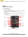
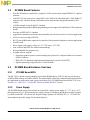
ZCOMM Board Description
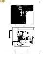
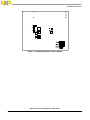
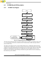
3.1 Board Overview . . . . . . . . . . . . . . . . . . . . . . . . . . . . . . . . . . . . . . . . . . . . . . . . . . . . . . . 1-1
3.2 ZCOMM Board Features . . . . . . . . . . . . . . . . . . . . . . . . . . . . . . . . . . . . . . . . . . . . . . . . 1-3
3.3 ZCOMM Board Hardware Overview . . . . . . . . . . . . . . . . . . . . . . . . . . . . . . . . . . . . . . . . 1-3
3.3.1 ZCOMM Board MCU . . . . . . . . . . . . . . . . . . . . . . . . . . . . . . . . . . . . . . . . . . . . . 1-3
3.3.2 Power Supply. . . . . . . . . . . . . . . . . . . . . . . . . . . . . . . . . . . . . . . . . . . . . . . . . . . 1-3
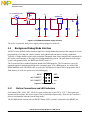
3.4 Background Debug Mode Interface . . . . . . . . . . . . . . . . . . . . . . . . . . . . . . . . . . . . . . . . 1-4
3.4.1 Button Connections and LED Indicators . . . . . . . . . . . . . . . . . . . . . . . . . . . . . . 1-4
3.4.2 Serial Communication (RS232 Interface) . . . . . . . . . . . . . . . . . . . . . . . . . . . . . 1-5
3.4.3 MC13213 RF Interface . . . . . . . . . . . . . . . . . . . . . . . . . . . . . . . . . . . . . . . . . . . 1-6
3.4.4 Clock Configuration . . . . . . . . . . . . . . . . . . . . . . . . . . . . . . . . . . . . . . . . . . . . . . 1-7
3.4.5 ZCOMM Board Power Connections . . . . . . . . . . . . . . . . . . . . . . . . . . . . . . . . . 1-7
3.4.6 Application Connector . . . . . . . . . . . . . . . . . . . . . . . . . . . . . . . . . . . . . . . . . . . . 1-8
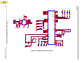
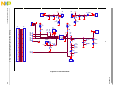
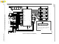
3.4.7 Schematic . . . . . . . . . . . . . . . . . . . . . . . . . . . . . . . . . . . . . . . . . . . . . . . . . . . . . 1-9
3.4.8 PCB Layout . . . . . . . . . . . . . . . . . . . . . . . . . . . . . . . . . . . . . . . . . . . . . . . . . . . . 1-9
Chapter 4
Demo System Description
4.1 General System Concept . . . . . . . . . . . . . . . . . . . . . . . . . . . . . . . . . . . . . . . . . . . . . . . . 1-1
4.2 High-Brightness LED Demo System Concept . . . . . . . . . . . . . . . . . . . . . . . . . . . . . . . . 1-1
4.2.1 Communication . . . . . . . . . . . . . . . . . . . . . . . . . . . . . . . . . . . . . . . . . . . . . . . . . 1-2
4.2.2 LIN Transceiver Board. . . . . . . . . . . . . . . . . . . . . . . . . . . . . . . . . . . . . . . . . . . . 1-2

Remote Control of High-Brightness LEDs, Rev. 0
Freescale Semiconductor II
4.3 Features . . . . . . . . . . . . . . . . . . . . . . . . . . . . . . . . . . . . . . . . . . . . . . . . . . . . . . . . . . . . . 1-2
4.3.1 Quadrunner Lumiled Demo Board. . . . . . . . . . . . . . . . . . . . . . . . . . . . . . . . . . . 1-4
Chapter 5
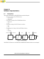
Software Implementation
5.1 Introduction. . . . . . . . . . . . . . . . . . . . . . . . . . . . . . . . . . . . . . . . . . . . . . . . . . . . . . . . . . . 1-1
5.2 ZCOMM Board S/W Description. . . . . . . . . . . . . . . . . . . . . . . . . . . . . . . . . . . . . . . . . . . 1-2
5.2.1 ZCOMM Flow Diagram . . . . . . . . . . . . . . . . . . . . . . . . . . . . . . . . . . . . . . . . . . . 1-2
5.2.2 ZCOMM SCI Data Format . . . . . . . . . . . . . . . . . . . . . . . . . . . . . . . . . . . . . . . . . 1-3
5.2.3 ZCOMM RF Protocol . . . . . . . . . . . . . . . . . . . . . . . . . . . . . . . . . . . . . . . . . . . . . 1-4
Chapter 6
Demo Setup
6.1 Introduction. . . . . . . . . . . . . . . . . . . . . . . . . . . . . . . . . . . . . . . . . . . . . . . . . . . . . . . . . . . 1-1
6.2 Setup Instructions and User Guide for Controlling the HB LED Demo System . . . . . . . 1-1
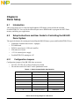
6.2.1 Configuration Jumpers. . . . . . . . . . . . . . . . . . . . . . . . . . . . . . . . . . . . . . . . . . . . 1-1
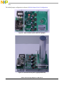
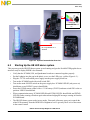
6.3 Starting Up the HB LED demo system . . . . . . . . . . . . . . . . . . . . . . . . . . . . . . . . . . . . . . 1-3
6.3.1 Troubleshooting. . . . . . . . . . . . . . . . . . . . . . . . . . . . . . . . . . . . . . . . . . . . . . . . . 1-4
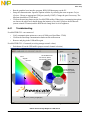
6.4 FreeMASTER GUI . . . . . . . . . . . . . . . . . . . . . . . . . . . . . . . . . . . . . . . . . . . . . . . . . . . . . 1-4
6.4.1 Troubleshooting. . . . . . . . . . . . . . . . . . . . . . . . . . . . . . . . . . . . . . . . . . . . . . . . . 1-5
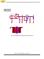
Appendix A
Schematics
Appendix B
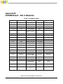
ZCOMM Board – Bill of Materials

Remote Control of High-Brightness LEDs, Rev. 0
Freescale Semiconductor 1-1
Chapter 1
Introduction
1.1 Introduction
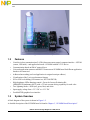
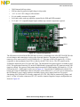
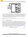
This document describes the design of a high-brightness LED demo system, which demonstrates wireless
communication using Freescale’s MC13213 (SiP) device, high-brightness LED dimming control using
Freescale’s MM908E625 (Quad Half H-Bridge with power supply + HC08), and the 3-axis acceleration
sensor MMA7260QT from Freescale.
This demo system is a versatile remote control for different applications. For the application in this demo,
the Freescale Luxeon Evaluation Kit by Future Electronics, with an HB LED board, was chosen.
Wireless communication is preferable because it provides flexibility in the positioning of application
devices without a wire medium. Light emitting diodes (LEDs) are popular in general lighting areas.
Advantages of using LED lighting are a long operating life, no fragile glass, no mercury, and low-voltage
DC operation.
The HB LED demo system performs light dimming on the red, green, blue, and white high-brightness
LEDs depending on the 3-axis acceleration sensor (MMA7260Q) readings on the ZSTAR remote control.
This design uses boards already available, such as the RD3152MMA7260Q (ZSTAR), Freescale Luxeon
Evaluation Kit by Future Electronics, and the LIN evaluation kit. The wireless communication board, the
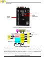
ZCOMM (wireleZ-COMMunication) board, is a newly designed board.
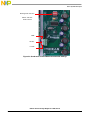
The current device ZCOMM board introduces users to the MC13213 low-cost 8-bit microcontroller with
2.4 GHz wireless data transceiver. It includes a universal application connector used for direct connection
to the application board, an RS232 port for communication with a control device, a background debug
module BDM, for in-circuit hardware debugging and programming, switches, LEDs for monitoring
purposes, and a host MCU, allowing the user flexibility in establishing wireless data networks between
various electrical applications.
This reference design includes basic radio freqency theory, the system design concept, hardware
implementation, and the software design, including the FreeMASTER software visualization tool.
Each wireless part communicates over the RF medium using the freely available software stack SMAC
from Freescale.

Introduction
Remote Control of High-Brightness LEDs, Rev. 0
1-2 Freescale Semiconductor
Figure 1-1. HB LED Demo System
1.2 Features
• Versitile wireless communication (2.4 GHz) between remote control, computer interface—ZSTAR
(sensor, USB stick)—and application board—ZCOMM with MC13213 device
• Communication based on SMAC protocol layer
• Universal application connector and RS232 connector on ZCOMM board for different application
boards to be connected
• Addressed networking (each end application is assigned a unique address)
• Visualization of the 3-axis accelerometer features
• SCI to LIN level shifting (LIN transceiver, KIT33661DEVB)
• High-brightness LEDs dimming control—Freescale Luxeon Evaluation Kit
(MM908E625Quadrunner MCU) with a 370 mA current driving capability for each color
• Two lightning modes—RGB (red, green, blue) and white
• Input supply voltage from +3.5 V DC to +12 V DC
• FreeMASTER graphical user interface
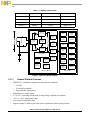
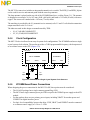
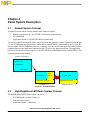
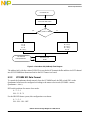
1.3 System Overview
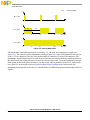
A block diagram of the system is shown in Figure 1-2.
A detailed description of the ZCOMM board is found in Chapter 3, “ZCOMM Board Description”.

Introduction
Remote Control of High-Brightness LEDs, Rev. 0
Freescale Semiconductor 1-3
Figure 1-2. High-Brightness LED Demo System Block Diagram
1.4 Featured Products
This demo consists of several Freescale products. Their main features are listed below.
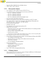
1.4.1 MC13213—2.4 GHz RF Transceiver and 8-Bit MCU
The MC1321x family is Freescale’s second-generation ZigBee
™
platform, which incorporates a
low-power 2.4 GHz radio frequency transceiver and an 8-bit microcontroller on a single 9x9x1 mm 71-pin
LGA package.
The MC1321x solution can be used for wireless applications from simple proprietary point-to-point
connectivity to a complete ZigBee mesh network. The combination of the radio and a microcontroller in
a small footprint package allows for a cost-effective solution. The MC1321x contains an RF transceiver
that is an IEEE 802.15.4-compliant radio that operates in the 2.4 GHz ISM frequency band. The
transceiver includes a low-noise amplifier, 1 mW nominal output power, PA with internal voltage
controlled oscillator (VCO), integrated transmit/receive switch, on-board power supply regulation, and
full spread-spectrum encoding and decoding.
The MC1321x also contains a microcontroller based on the HCS08 family of microcontrollers and can
provide up to 60 KB of flash memory and 4 KB of RAM. The onboard MCU allows the communications
stack and also the application to reside on the same system-in-package (SiP). Table 1-1 shows the
MC1321x family organization.

Introduction
Remote Control of High-Brightness LEDs, Rev. 0
1-4 Freescale Semiconductor
Figure 1-3. MC13213 Block Diagram
1.4.1.1 General Platform Features
• IEEE 802.15.4 standard compliant on-chip transceiver/modem
— 2.4 GHz
— 16 selectable channels
— Programmable output power
• Multiple power saving modes
• 2 V to 3.4 V operating voltage with on-chip voltage regulators for modem
• –40°C to +85°C temperature range
• Low external component count
• Supports single 16 MHz crystal clock source operation or dual crystal operation
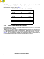
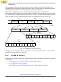
Table 1-1. Memory Configuration
Microcontroller Program Flash Unified Data/Program RAM Extended Features
MC13211 16 Kbyte 1 Kbyte —
MC13212 32 Kbyte 2 Kbyte —
MC13213 60 Kbyte 4 Kbyte —
MC13214 60 Kbyte 4 Kbyte ZigBee stack
Transmmit
receive
switch
Frequency
generator
Analog
receiver
Analog
transmitter
RFIC
timers
Digital
control
logic
SPI
7 GPIO
Buffer RAM
IRQ arbiter
RAM arbiter
Power
mangement
Voltage
regulators
HCS08
CPU
Background
debug
mode
Flash
memory
8 Channel
10 Bit ADC
RAM
2xSCI
Dedicated
SPI
I2C
Low
voltage
interrupt
16 Bit
Timers
Keyboard
interrupt
COP
Internal
clock
generator
Up to 32
GPIOs
802.15.4 Modem
HCS08 MCU
CT_Bias

Introduction
Remote Control of High-Brightness LEDs, Rev. 0
Freescale Semiconductor 1-5
• Support for SMAC, IEEE 802.15.4, and ZigBee software
• 9 mm x 9 mm x 1 mm 71-pin LGA
1.4.1.2 Microcontroller Features
• Low-voltage MCU with a 40 MHz low-power HCS08 CPU core
• Up to 60K flash memory with block protection and security and 4K RAM
— MC13211: 16 KB flash, 1 KB RAM
— MC13212: 32 KB flash, 2 KB RAM
— MC13213: 60 KB flash, 4 KB RAM
— MC13214: 60 KB flash, 4 KB RAM with ZigBee Z-stack
• Low-power modes (Wait and three stop modes)
• Dedicated serial peripheral interface (SPI) connected internally to an 802.15.4 modem
• One 4-channel and one 1-channel 16-bit timer/pulse-width modulator (TPM) module with
selectable input capture, output capture, and PWM capability
• 8-bit port keyboard interrupt (KBI)
• 8-channel 8-10-bit ADC
• Two independent serial communication interfaces (SCI)
• Multiple clock source options
— Internal clock generator (ICG) with a 243 kHz oscillator that has ±0.2% trimming resolution
and ±0.5% deviation across voltage.
— Start-up oscillator of approximately 8 MHz
— External crystal or resonator
— External source from the modem clock for high accuracy source or a low-cost system option
• Inter-integrated circuit (IIC) interface with 100 kbps operation
• In-circuit debug and flash programming available via on-chip background debug module (BDM)
— Two comparator and nine trigger modes
— Eight deep FIFO for storing change-of-flow addresses and event-only data
— Tag and force breakpoints
— In-circuit debugging with single breakpoint
• System protection features
— Programmable low voltage interrupt (LVI)
— Optional watchdog timer (COP)
— Illegal opcode detection
• Up to 32 MCU GPIOs with programmable pull-ups
1.4.1.3 RF Modem Features
• Fully compliant IEEE 802.15.4 transciever supports 250 kbps O-QPSK data in 5.0 MHz channels
and full spread-spectrum encode and decode

Introduction
Remote Control of High-Brightness LEDs, Rev. 0
1-6 Freescale Semiconductor
• Operates on one of 16 selectable channels in the 2.4 GHz ISM band
• –1 to 0 dBm nominal output power, programmable from –27 dBm to +3 dBm typical
• Receive sensitivity of ≤92 dBm (typical) at 1% PER, 20-byte packet, much better than the IEEE
802.15.4 specification of –85 dBm
• Integrated transmit/receive switch
• Dual PA output pairs that can be programmed for full differential single port or dual port operation
that supports an external LNA and/or PA
• Three low-power modes for increased battery life
• Programmable frequency clock output for use by the MCU
• Onboard trim capability for the 16 MHz crystal reference oscillator eliminates the need for external
variable capacitors and allows for automated production frequency calibration
• Four internal timer comparators available to supplement the MCU timer resources
• Supports packet mode and streaming mode
• Seven GPIOs to supplement the MCU GPIO
1.4.2 MM908E625 – Integrated Quad Half H-Bridge with Power Supply
The 908E625 is an integrated single-package solution including a high-performance HC08
microcontroller with a SMARTMOS™ analog control IC. The HC08 includes flash memory, a timer,
enhanced serial communications interface (ESCI), an analog-to-digital converter (ADC), serial peripheral
interface (SPI) (only internal), and an internal clock generator (ICG) module. The analog control die
provides fully protected H-Bridge/high-side outputs, voltage regulator, autonomous watchdog with cyclic
wake-up, and a local interconnect network (LIN) physical layer. The single-package solution, together
with the LIN, provides optimal application performance adjustments and space-saving PCB design. It is
suited for the control of automotive mirror, doorlock, and light-leveling applications.
1.4.2.1 MM908E625 Features
• High-performance M68HC908EY16 core
• 16 KB of on-chip flash memory
• 512 bytes of RAM
• Internal clock generation module
• Two 16-bit, 2-Channel Timers
• 10-bit analog-to-digital converter
• LIN physical layer
• Autonomous watchdog with cyclic wakeup
• Three two-terminal hall-effect sensor input ports
• One analog input with switchable current source
• Four low RDS(ON) half-bridge outputs
• One low RDS(ON) high-side output
• 13 microcontroller I/Os

Introduction
Remote Control of High-Brightness LEDs, Rev. 0
Freescale Semiconductor 1-7
1.4.3 Triple Axis Accelerometer MMA7260QT
The MMA7260QT is a low-g accelerometer with a selectable 1.5 g to 6 g range. The MMA7260QT has
many unique features that make it an ideal solution for many consumer applications, such as freefall
protection for laptops and MP3 players, tilt detection for e-compass compensation and mobile phone
scrolling, motion detection for handheld games and game controllers, position sensing for g-mice, shock
detection for warranty monitors, and vibration for out of balance detection. Features such as low power,
low current, and a sleep mode with a quick turn on time, allow the battery life to be extended in end
applications. The 3-axis sensing in a small QFN package requires a 6mm x 6mm board space, with a
profile of 1.45 mm, allowing easy integration into many small handheld electronics.
There are several other derivatives of the MMA7260QT:
• • MMA7261QT XYZ-axis 2.5g/3.3g/6.7g/10g
• • MMA6270QT XY-axis 1.5g/2g/4g/6g
• • MMA6271QT XY-axis 2.5g/3.3g/6.7g/10g
• • MMA6280QT XZ-axis 1.5g/2g/4g/6g
• • MMA6281QT XZ-axis 2.5g/3.3g/6.7g/10g
All members of this sensor family are footprint (QFN package) compatible, which simplifies evaluation
and design of the target application.

Introduction
Remote Control of High-Brightness LEDs, Rev. 0
1-8 Freescale Semiconductor

Remote Control of High-Brightness LEDs, Rev. 0
Freescale Semiconductor 2-1
Chapter 2
Control Theory for HBLED Lighting
2.1 Switching Regulator
A switching regulator regulates a current flow by dividing the input voltage and controlling the average
current by means of the duty cycle. When a higher load current is required by the load, the percentage of
on-time is increased to accommodate the change. There are two basic types of switching regulators:
forward-mode regulators and flyback-mode regulators. The name of each type is derived from the way the
magnetic elements are used within the regulator. In this design, forward-mode switching is used and you
can find the theory below.
Forward-mode switching regulators have four functional components: a power switch, a rectifier, a series
inductor, and a capacitor (see Figure 2-1). The power switch may be a power transistor or a metal oxide
semiconductor field-effect transistor (MOSFET) placed directly between the input voltage and the LC
filter section. The shunt diode, series inductor, and shunt capacitor form an energy storage tank whose
purpose is to store enough energy to maintain the load voltage and current over the entire off-time of the
power switch. The power switch serves only to fill up the energy lost to the load during its off-time.
Flyback-mode switching regulators have the same four basic elements as the forward-mode regulators
except that they have been rearranged in another configuration.
Figure 2-1. Forward Mode Switching Regulator
2.2 Buck Converter Basics
A buck, or step-down converter, is the most elementary forward-mode converter. Figure 2-1shows its basic
schematic.
The operation of this regulator topology has two distinct time periods. The first occurs when the series
switch SW1 is on, the input voltage V
in
is connected to the input of the inductor (L). The output of the
inductor is the output voltage, and the rectifier (or catch diode) is reverse biased. During this period,
Vin
L
D
SW1
Co
RL

Control Theory for HBLED Lighting
Remote Control of High-Brightness LEDs, Rev. 0
2-2 Freescale Semiconductor
because there is a constant voltage source connected across the inductor, the inductor current begins to
linearly ramp upwards, as described by the following equation:
IL(on) = [(Vin – Vout) x ton] / L Eqn. 2-1
During this on period, energy is stored within the core material in the form of magnetic flux. If the inductor
is properly designed, there is sufficient energy stored to carry the requirements of the load during the off
period.
The next period is the off period of the power switch. When the power switch turns off, the voltage across
the inductor reverses its polarity and is clamped at one diode voltage drop below ground by the catch diode.
The current flows through the catch diode, thus maintaining the load current loop. This removes the stored
energy from the inductor. The inductor current during this time is:
IL(off) = [(Vout – VD) x toff] / L Eqn. 2-2
This period ends when the power switch is turned on again. Regulation of the converter is accomplished
by varying the duty cycle of the power switch according to the loading conditions. To achieve this, the
power switch requires electronic control for proper operation. It is possible to describe the duty cycle as:
d = ton / T Eqn. 2-3
where T is the switching period.
For the buck converter with ideal components, the duty cycle can also be described as:
d = Vout / Vin Eqn. 2-4
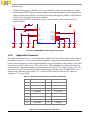
2.3 MM908E625 Driving High Brightness LED’s Basics
This section contains a brief introduction to the basic circuit design used to drive the high-brightness LEDs
using the MM908E625 integrated quad half H-bridge with power supply, embedded MCU, and LIN serial
communication.
The main idea behind the circuit design to control the amount of current flowing through the high
brightness LEDs is to implement a type of step-down buck regulator, controlling the current instead of the
voltage output. Taking advantage of the low-side MOSFET current limit feature of the MM908E625
simplifies the overall design.
The circuit configuration in Figure 2-2 illustrates the basic operation of the current regulator.

Control Theory for HBLED Lighting
Remote Control of High-Brightness LEDs, Rev. 0
Freescale Semiconductor 2-3
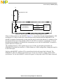
Figure 2-2. Basic Circuit Used to Drive the High Brightness LEDs
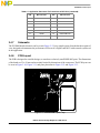
When switching on the low-side MOSFET (Figure 2-3), current flows through the high-brightness LED
and inductor (L). When it reaches the current limit previously defined inside the MM908E625, the
MOSFET is turned off automatically. At this point, the energy stored in the inductor (L) continues to flow
through the LED because of the Schottky diode (D). The idea is to maintain a constant flow of current
through the high-brightness LED. Before the current drops to zero, the low-side MOSFET is turned on
again to start a new current cycle.
The switching frequency of the regulator was set up at 25 kHz. It is internally generated by the
MM908E625 using the timer interface A (TIMA) module in a PWM configuration, feeding this signal in
to the FGEN input.
Each low-side MOSFET switches off if a current above the selected current limit is detected. The
MM908E625 offers five different current limits, the 370 mA was selected to comply with the LED's
specification. The low-side MOSFET switches ON again if a rising edge on the FGEN input is detected.
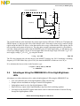
Control
Low-side driver
current limitation
On/off
Status
Current limit
GND
HBx
D
High-brightness LED
V+
908E625 Internal circuit
L

Control Theory for HBLED Lighting
Remote Control of High-Brightness LEDs, Rev. 0
2-4 Freescale Semiconductor
Figure 2-3. Low-Side MOSFET Switching on the MM908E625 to Drive the High-Brightness LEDs
2.4 Selection of Inductor L for Driving the High- Brightness LEDs
Looking closely at the specifications of the device, there is a feature essential to this application. Each of
the four half-bridge outputs has a programmable current limit mode of operation when the low-side
MOSFETs are used in PWM mode. This limit is implemented by turning off the MOSFET on a
cycle-by-cycle basis after it reaches the preset current limit (Figure 2-3). In this application, the low side
MOSFET conduction is activated on the rising edge of a base clock provided by the MCU. The MOSFET
is on until the current limit is reached, at which time the limit circuit terminates the current cycle, turning
off the MOSFET. Driving only the LED in this mode would not work properly because the current limit
would be reached quickly and the MOSFET would turn off. An inductor is used to limit the speed of
current change in the circuit (di/dt), effectively creating an efficient 4-channel buck switching current
regulator.
The maximum low-side PWM clock frequency specification for the MM908E625 is 25 KHz. This rate is
easily provided by the MCU timer output. TimerA CH1 (PTD1/TACH1) is used as a programmable
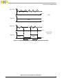
25 KHz clock source, driving the signal FGEN that controls the MOSFET conduction period (Figure 2-4).
40us
Time
Time
OFF
OFF
OFF
ONON
ON
370 mA
DC component
Low-side MOSFET
HB low-side MOSFET turns on
with each rising edge of the FGEN input
HB low-side MOSFET is switched off
when it reaches the selected current limit
FGEN input
(MCU PWM signal)
Half-bridge
Low-side output
ILS
ID
ID
ILS
current
Diode current

Control Theory for HBLED Lighting
Remote Control of High-Brightness LEDs, Rev. 0
Freescale Semiconductor 2-5
Figure 2-4. MM908E625 H-Bridge Output
The external inductor value determines the current ripple into the LED at the 25 KHz rate. The higher the
PWM frequency is, the lower the value of the inductor can be. Selecting a value too low results in a high
ripple current into the LED. Select a value that satisfies the average current that the LED requires, but do
not exceed the peak current of the device. The only other external component required is a fast diode to
catch the voltage spike that results when the MOSFET turns off. In this application, a 1 mH inductor was
selected, providing roughly 150 mA of current ripple ΔIPP when driving a single LED with a V
f
of 3.8 V
and a supply voltage V
L
of +12 V
dc
by using the formula:
L = (V
L
* Δt) / ΔIPP Eqn. 2-5
The Δt is the charging time, the time the low-side MOSFET switches stay ON. Considering a switching
frequency of 25 kHz with a duty cycle of 50%, the time the MOSFET switches are on is 20 μs.
If we substitute the known values in the formula we get:
L = ((12 V – 3.8 V) * 20 μs) / 150 mA
L = 1.093 mH Eqn. 2-6
2.5 Advantages Using the MM908E625 to Drive High-Brightness
LEDs
Advantages over other solutions to drive today's high brightness LEDs using the MM908E625 are:
• Low-cost solution to drive four high brightness LEDs with one chip
• Simple software and hardware design to control LED brightness
• Independent control over the four high-brightness LEDs
• High efficiency output control implementing a step-down buck switching regulator
• On-chip low-side MOSFET current limit feature used to control the amount of current flowing
through the high brightness LEDs
S
R
Flip Flop
Fgen
-
+
Q
Vref
Rc
LED
D
L
Vs
Internal to MM908E625

Control Theory for HBLED Lighting
Remote Control of High-Brightness LEDs, Rev. 0
2-6 Freescale Semiconductor
• Low heat generation due to the use of the MM908E625 internal power MOSFETs with low RDS(ON)
• RF communication can be established interfacing to a ZCOMM board by emulating SCI
communication
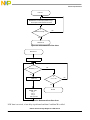
2.6 Dimming the Four High-Brightness LEDs
A PWM mechanism was chosen for dimming the four LEDs. Having set the maximum current through the
LEDs, by switching on and off the low-side MOSFETs using the FGEN signal and taking advantage of the
current limit feature on the MM908E625 ( Figure 2-4).
NOTE
If a 100% brightness is required, it is only necessary to turn on the low-side
MOSFETs and have the automatic feature to take place. If a percentage
different than full brightness is required, switch on and off the driving of the
LEDs. This needs to be done at a low frequency with a certain duty cycle to
generate a dimming sensation to the human eye, reducing the amount of
current flowing through the LED over time.
The recommended refresh frequency for this PWM can be from 75 Hz to 100 Hz, to avoid any flickering
sensation to the human eye. Also, it was decided to have a 20-step resolution for the duty cycle to keep the
whole implementation as simple as possible.
Figure 2-5 shows a graphical representation of the PWM implementation used to dim the high brightness
LEDs.
Each of the MM908E625’s four half-bridge outputs has a programmable current limit mode of operation
when the low-side MOSFETs are used in PWM mode. This limit is implemented by turning off the
MOSFET on a cycle-by-cycle basis after it reaches the pre-set current limit (Figure 2-3). In this
application, the low-side MOSFET conduction is activated on the rising edge of a base clock provided by
the MCU. The MOSFET is on until the current limit is reached, at which time the limit circuit terminates
the current cycle, turning off the MOSFET. Driving only the LED in this mode does not work properly
because the current limit is reached quickly and the MOSFET turns off. An inductor is used to limit the
speed of current change in the circuit (di/dt), effectively creating an efficient 4-channel buck switching
current regulator.
The maximum low-side PWM clock frequency specification for the MM908E625 is 25 KHz. This rate is
easily provided by the MCU timer output. TimerA CH1 (PTD1/TACH1) is used as a programmable
25 KHz clock source, driving the signal FGEN that controls the MOSFET conduction period.

Control Theory for HBLED Lighting
Remote Control of High-Brightness LEDs, Rev. 0
Freescale Semiconductor 2-7
Figure 2-5. PWM Implementation for Dimming the High-Brightness LEDs
LED current
Time
Time
100%
LED current
Time
Time
100%
100%
10ms
Duty Cycle
Duty Cycle
100%
Results in 50%
duty cycle

Control Theory for HBLED Lighting
Remote Control of High-Brightness LEDs, Rev. 0
2-8 Freescale Semiconductor
Page is loading ...
Page is loading ...
Page is loading ...
Page is loading ...
Page is loading ...
Page is loading ...
Page is loading ...
Page is loading ...
Page is loading ...
Page is loading ...
Page is loading ...
Page is loading ...
Page is loading ...
Page is loading ...
Page is loading ...
Page is loading ...
Page is loading ...
Page is loading ...
Page is loading ...
Page is loading ...
Page is loading ...
Page is loading ...
Page is loading ...
Page is loading ...
Page is loading ...
Page is loading ...
Page is loading ...
Page is loading ...
Page is loading ...
Page is loading ...
Page is loading ...
Page is loading ...
Page is loading ...
Page is loading ...
Page is loading ...
Page is loading ...
Page is loading ...
Page is loading ...
Page is loading ...
Page is loading ...
-
 1
1
-
 2
2
-
 3
3
-
 4
4
-
 5
5
-
 6
6
-
 7
7
-
 8
8
-
 9
9
-
 10
10
-
 11
11
-
 12
12
-
 13
13
-
 14
14
-
 15
15
-
 16
16
-
 17
17
-
 18
18
-
 19
19
-
 20
20
-
 21
21
-
 22
22
-
 23
23
-
 24
24
-
 25
25
-
 26
26
-
 27
27
-
 28
28
-
 29
29
-
 30
30
-
 31
31
-
 32
32
-
 33
33
-
 34
34
-
 35
35
-
 36
36
-
 37
37
-
 38
38
-
 39
39
-
 40
40
-
 41
41
-
 42
42
-
 43
43
-
 44
44
-
 45
45
-
 46
46
-
 47
47
-
 48
48
-
 49
49
-
 50
50
-
 51
51
-
 52
52
-
 53
53
-
 54
54
-
 55
55
-
 56
56
-
 57
57
-
 58
58
-
 59
59
-
 60
60


NXP MM908E625 Reference guide
- Type
- Reference guide
Ask a question and I''ll find the answer in the document
Finding information in a document is now easier with AI
Related papers
Other documents
-
Freescale Semiconductor MC9S12VR64 Reference guide
-
-
-
-
Alps Electric Virtual Cable Light Module User manual
-
NXP Semiconductors KEA128LEDLIGHTRD Installation Instructions Manual
-
-
-
Silicon Labs Si484x-Demo Board User guide
-