
Document Number: MC1321xEVKRM
Rev. 1.2
04/2008
MC1321x Evaluation Kit (EVK)
Reference Manual

How to Reach Us:
Home Page:
www.freescale.com
E-mail:
support@freescale.com
USA/Europe or Locations Not Listed:
Freescale Semiconductor
Technical Information Center, CH370
1300 N. Alma School Road
Chandler, Arizona 85224
+1-800-521-6274 or +1-480-768-2130
support@freescale.com
Europe, Middle East, and Africa:
Freescale Halbleiter Deutschland GmbH
Technical Information Center
Schatzbogen 7
81829 Muenchen, Germany
+44 1296 380 456 (English)
+46 8 52200080 (English)
+49 89 92103 559 (German)
+33 1 69 35 48 48 (French)
support@freescale.com
Japan:
Freescale Semiconductor Japan Ltd.
Headquarters
ARCO Tower 15F
1-8-1, Shimo-Meguro, Meguro-ku,
Tokyo 153-0064, Japan
0120 191014 or +81 3 5437 9125
support.jap[email protected]
Asia/Pacific:
Freescale Semiconductor Hong Kong Ltd.
Technical Information Center
2 Dai King Street
Tai Po Industrial Estate
Tai Po, N.T., Hong Kong
+800 2666 8080
support.asia@freescale.com
For Literature Requests Only:
Freescale Semiconductor Literature Distribution Center
P.O. Box 5405
Denver, Colorado 80217
1-800-521-6274 or 303-675-2140
Fax: 303-675-2150
LDCForFreescaleSemiconductor@hibbertgroup.com
Information in this document is provided solely to enable system and software implementers to use
Freescale Semiconductor products. There are no express or implied copyright licenses granted
hereunder to design or fabricate any integrated circuits or integrated circuits based on the information
in this document.
Freescale Semiconductor reserves the right to make changes without further notice to any products
herein. Freescale Semiconductor makes no warranty, representation or guarantee regarding the
suitability of its products for any particular purpose, nor does Freescale Semiconductor assume any
liability arising out of the application or use of any product or circuit, and specifically disclaims any
and all liability, including without limitation consequential or incidental damages. “Typical” parameters
that may be provided in Freescale Semiconductor data sheets and/or specifications can and do vary
in different applications and actual performance may vary over time. All operating parameters,
including “Typicals”, must be validated for each customer application by customer’s technical
experts. Freescale Semiconductor does not convey any license under its patent rights nor the rights
of others. Freescale Semiconductor products are not designed, intended, or authorized for use as
components in systems intended for surgical implant into the body, or other applications intended to
support or sustain life, or for any other application in which the failure of the Freescale Semiconductor
product could create a situation where personal injury or death may occur. Should Buyer purchase
or use Freescale Semiconductor products for any such unintended or unauthorized application,
Buyer shall indemnify and hold Freescale Semiconductor and its officers, employees, subsidiaries,
affiliates, and distributors harmless against all claims, costs, damages, and expenses, and
reasonable attorney fees arising out of, directly or indirectly, any claim of personal injury or death
associated with such unintended or unauthorized use, even if such claim alleges that Freescale
Semiconductor was negligent regarding the design or manufacture of the part.
Freescale™ and the Freescale logo are trademarks of Freescale Semiconductor, Inc. All other
product or service names are the property of their respective owners.
© Freescale Semiconductor, Inc. 2004, 2005, 2006, 2007, 2008. All rights reserved.

MC1321xEVK Reference Manual, Rev. 1.2
Freescale Semiconductor iii
Contents
About This Book
Audience. . . . . . . . . . . . . . . . . . . . . . . . . . . . . . . . . . . . . . . . . . . . . . . . . . . . . . . . . . . . . . . . . . . . iii
Organization . . . . . . . . . . . . . . . . . . . . . . . . . . . . . . . . . . . . . . . . . . . . . . . . . . . . . . . . . . . . . . . . . iii
Revision History . . . . . . . . . . . . . . . . . . . . . . . . . . . . . . . . . . . . . . . . . . . . . . . . . . . . . . . . . . . . . . iv
Definitions, Acronyms, and Abbreviations . . . . . . . . . . . . . . . . . . . . . . . . . . . . . . . . . . . . . . . . . iv
References. . . . . . . . . . . . . . . . . . . . . . . . . . . . . . . . . . . . . . . . . . . . . . . . . . . . . . . . . . . . . . . . . . . . v
Chapter 1
Safety Information
1.1 FCC Guidelines. . . . . . . . . . . . . . . . . . . . . . . . . . . . . . . . . . . . . . . . . . . . . . . . . . . . . . . . . . . . . . 1-1
1.1.1 47 C.F.R. Sec. 15.21. . . . . . . . . . . . . . . . . . . . . . . . . . . . . . . . . . . . . . . . . . . . . . . . . . . . . . . 1-1
1.1.2 47 C.F.R. Sec.15.105(b) . . . . . . . . . . . . . . . . . . . . . . . . . . . . . . . . . . . . . . . . . . . . . . . . . . . . 1-1
1.1.3 47 C.F.R. Sec.15.203 . . . . . . . . . . . . . . . . . . . . . . . . . . . . . . . . . . . . . . . . . . . . . . . . . . . . . . 1-2
1.2 Disposal Instructions. . . . . . . . . . . . . . . . . . . . . . . . . . . . . . . . . . . . . . . . . . . . . . . . . . . . . . . . . . 1-2
Chapter 2
System Overview
2.1 MC1321x Solution . . . . . . . . . . . . . . . . . . . . . . . . . . . . . . . . . . . . . . . . . . . . . . . . . . . . . . . . . . . 2-2
2.2 General-Purpose I/O and Peripheral Ports . . . . . . . . . . . . . . . . . . . . . . . . . . . . . . . . . . . . . . . . . 2-3
2.3 Power-Saving Modes . . . . . . . . . . . . . . . . . . . . . . . . . . . . . . . . . . . . . . . . . . . . . . . . . . . . . . . . . 2-5
2.4 Clock. . . . . . . . . . . . . . . . . . . . . . . . . . . . . . . . . . . . . . . . . . . . . . . . . . . . . . . . . . . . . . . . . . . . . . 2-6
2.5 Background Debug Module (BDM) Interface . . . . . . . . . . . . . . . . . . . . . . . . . . . . . . . . . . . . . . 2-6
2.6 Reset . . . . . . . . . . . . . . . . . . . . . . . . . . . . . . . . . . . . . . . . . . . . . . . . . . . . . . . . . . . . . . . . . . . . . . 2-6
Chapter 3
RF Front End
3.1 RF Transceiver . . . . . . . . . . . . . . . . . . . . . . . . . . . . . . . . . . . . . . . . . . . . . . . . . . . . . . . . . . . . . . 3-1
3.1.1 DC Biasing . . . . . . . . . . . . . . . . . . . . . . . . . . . . . . . . . . . . . . . . . . . . . . . . . . . . . . . . . . . . . . 3-1
3.2 RF Matching . . . . . . . . . . . . . . . . . . . . . . . . . . . . . . . . . . . . . . . . . . . . . . . . . . . . . . . . . . . . . . . . 3-1
3.3 On-board Antenna. . . . . . . . . . . . . . . . . . . . . . . . . . . . . . . . . . . . . . . . . . . . . . . . . . . . . . . . . . . . 3-2
3.4 Internal Power Supplies . . . . . . . . . . . . . . . . . . . . . . . . . . . . . . . . . . . . . . . . . . . . . . . . . . . . . . . 3-2
3.4.1 RF Section. . . . . . . . . . . . . . . . . . . . . . . . . . . . . . . . . . . . . . . . . . . . . . . . . . . . . . . . . . . . . . . 3-2
3.4.2 Digital Section . . . . . . . . . . . . . . . . . . . . . . . . . . . . . . . . . . . . . . . . . . . . . . . . . . . . . . . . . . . 3-2
3.5 Reference Oscillator . . . . . . . . . . . . . . . . . . . . . . . . . . . . . . . . . . . . . . . . . . . . . . . . . . . . . . . . . . 3-2
3.6 RF Performance . . . . . . . . . . . . . . . . . . . . . . . . . . . . . . . . . . . . . . . . . . . . . . . . . . . . . . . . . . . . . 3-3
3.6.1 TX Power . . . . . . . . . . . . . . . . . . . . . . . . . . . . . . . . . . . . . . . . . . . . . . . . . . . . . . . . . . . . . . . 3-3
3.6.2 Harmonics. . . . . . . . . . . . . . . . . . . . . . . . . . . . . . . . . . . . . . . . . . . . . . . . . . . . . . . . . . . . . . . 3-3
3.6.3 RX Sensitivity. . . . . . . . . . . . . . . . . . . . . . . . . . . . . . . . . . . . . . . . . . . . . . . . . . . . . . . . . . . . 3-3

MC1321xEVK Reference Manual, Rev. 1.2
iv Freescale Semiconductor
Chapter 4
MC1321xEVK Interfaces and Board Layout
4.1 Power Supply . . . . . . . . . . . . . . . . . . . . . . . . . . . . . . . . . . . . . . . . . . . . . . . . . . . . . . . . . . . . . . . 4-1
4.2 USB Interface . . . . . . . . . . . . . . . . . . . . . . . . . . . . . . . . . . . . . . . . . . . . . . . . . . . . . . . . . . . . . . . 4-1
4.3 RS-232 Interface. . . . . . . . . . . . . . . . . . . . . . . . . . . . . . . . . . . . . . . . . . . . . . . . . . . . . . . . . . . . . 4-2
4.4 Display . . . . . . . . . . . . . . . . . . . . . . . . . . . . . . . . . . . . . . . . . . . . . . . . . . . . . . . . . . . . . . . . . . . . 4-2
4.5 EEPROM (IC104). . . . . . . . . . . . . . . . . . . . . . . . . . . . . . . . . . . . . . . . . . . . . . . . . . . . . . . . . . . . 4-2
4.6 Sensors . . . . . . . . . . . . . . . . . . . . . . . . . . . . . . . . . . . . . . . . . . . . . . . . . . . . . . . . . . . . . . . . . . . . 4-3
4.6.1 XYZ Sensor (IC105). . . . . . . . . . . . . . . . . . . . . . . . . . . . . . . . . . . . . . . . . . . . . . . . . . . . . . . 4-3
4.6.2 Temperature Sensor (IC109) . . . . . . . . . . . . . . . . . . . . . . . . . . . . . . . . . . . . . . . . . . . . . . . . 4-3
4.6.3 Audio Indicator (PZ100). . . . . . . . . . . . . . . . . . . . . . . . . . . . . . . . . . . . . . . . . . . . . . . . . . . . 4-3
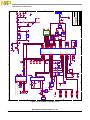
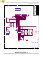
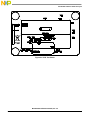
4.7 NCB Pinouts and Schematic. . . . . . . . . . . . . . . . . . . . . . . . . . . . . . . . . . . . . . . . . . . . . . . . . . . . 4-4
4.8 13213-SRB Pinouts and Schematic . . . . . . . . . . . . . . . . . . . . . . . . . . . . . . . . . . . . . . . . . . . . . . 4-8
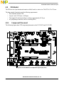
4.9 PCB Build. . . . . . . . . . . . . . . . . . . . . . . . . . . . . . . . . . . . . . . . . . . . . . . . . . . . . . . . . . . . . . . . . 4-11
4.9.1 Component Placement . . . . . . . . . . . . . . . . . . . . . . . . . . . . . . . . . . . . . . . . . . . . . . . . . . . . 4-11
4.9.2 Board Layouts. . . . . . . . . . . . . . . . . . . . . . . . . . . . . . . . . . . . . . . . . . . . . . . . . . . . . . . . . . . 4-14

MC1321xEVK Reference Manual, Rev. 1.2
Freescale Semiconductor iii
About This Book
This manual provides a detailed hardware description of the MC1321xEVK which consists of a
13213-Network Coordinator Board (13213-NCB) and a 13213-Sensor Reference Board (13213-SRB).
The functionality of the 13213-NCB and 13213-SRB boards is very similar. The primary difference
between the two boards revolves around the peripheral circuits, not in the reference design itself.
The 13213-NCB and 13213-SRB provide all the necessary components to evaluate and use the MC1321x
solution. The 13213-NCB and the 13213-SRB are built around the Freescale MC1321x family. The
MC1321x family is Freescale’s second-generation ZigBee platform which incorporates a low power 2.4
GHz radio frequency transceiver and an 8-bit microcontroller into a single 9x9x1 mm 71-pin LGA
package.
The 13213-NCB and the 13213-SRB are compliant with the following standards:
• FCC standard 47 CFR, part 15, section 15.247
• ETSI EN 300-328-1
• ETSI EN 300-328-2
Audience
This document is intended for software, hardware, and system engineers who are developing their products
or software applications making use of the MC1321x to achieve wireless connectivity capability. The
MC1321x is compliant with the IEEE 802.15.4 and the ZigBee standards.
Organization
This document is organized into four (4) chapters.
Chapter 1 Safety Information — This chapter describes the safety guidelines for the
MC1321xEVK.
Chapter 2 System Overview — This chapter introduces the basic components, functionality,
and power supply options of the MC1321xEVK boards.
Chapter 3 RF Front End — This chapter provides a description of the external analog
circuitry required to ensure proper MC1321x operation.
Chapter 4 MC1321xEVK Interfaces and Board Layout — This chapter briefly describes
the available interfaces between the EVBs and a personal computer (PC) and
provides schematics and component and board layout information.

MC1321xEVK Reference Manual, Rev. 1.2
iv Freescale Semiconductor
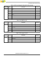
Revision History
The following table summarizes revisions to this document since the previous release (Rev. 1.1).
Definitions, Acronyms, and Abbreviations
The following list defines the acronyms and abbreviations used in this document.
ATD Analog To Digital
BDM Background Debug Module
CPU Central Processing Unit
EEPROM Electrical Erasable Programmable Read Only Memory
ESD Electro Static Discharge
EVB Evaluation Board
EVK Evaluation Kit
GPIO General Purpose Input Output
ICG Internal Clock Generation
LDO Low Drop Output
LNA Low Noise Amplifier
MCU Micro Controller Unit
NCB Network Coordinator Board
PA Power Amplifier
PC Personal Computer
PCB Printed Circuit Board
QFN Quad Flat Non-lead package
RAM Random Access Memory
RF Radio Frequency
Rx Receive
SCI Serial Communication Interface
SMA SubMiniature version A
SPI Serial Peripheral Interface
SRB Sensor Reference Board.
Tx Transmit
Revision History
Location Revision
Entire Document Various specification number updates
and transceiver information updates.

MC1321xEVK Reference Manual, Rev. 1.2
Freescale Semiconductor v
References
The following sources were referenced to produce this book:
[1] MC1321x Data Sheet, MC1321x
[2] MC1321x Reference Manual, MC1321xRM

MC1321xEVK Reference Manual, Rev. 1.2
vi Freescale Semiconductor

MC1321xEVK Reference Manual, Rev. 1.2
Freescale Semiconductor 1-1
Chapter 1
Safety Information
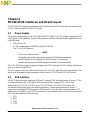
1.1 FCC Guidelines
Any modifications to this product may violate the rules of the Federal Communications Commission and
make operation of the product unlawful.
1.1.1 47 C.F.R. Sec. 15.21
This equipment has been tested and found to comply with the limits for a Class B digital device, pursuant
to part 15 of the FCC Rules. These limits are designed to provide reasonable protection against harmful
interference in a residential installation. This equipment generates, uses and can radiate radio frequency
energy and, if not installed and used in accordance with the instructions, may cause harmful interference
to radio communications. However, there is no guarantee that interference will not occur in a particular
installation. If this equipment does cause harmful interference to radio or television reception, which can
be determined by turning the equipment off and on, the user is encouraged to try to correct the interference
by one or more of the following measures:
• Reorient or relocate the receiving antenna.
• Increase the separation between the equipment and receiver.
• Connect the equipment into an outlet on a circuit different from that to which the receiver is
connected.
• Consult the dealer or an experienced radio/TV technician for help.
1.1.2 47 C.F.R. Sec.15.105(b)
This equipment complies with FCC radiation exposure limits set forth for an uncontrolled environment.
The antenna(s) used for this equipment must be installed to provide a separation distance of at least 8
inches (20cm) from all persons.
This device complies with Part 15 of the FCC Rules. Operation is subject to the following three
conditions:
1. This device may not cause harmful interference.
2. This device must accept any interference received, including interference that may cause undesired
operation.
3. This device is susceptible to electrostatic discharge (ESD) and surge phenomenon.

Safety Information
MC1321xEVK Reference Manual, Rev. 1.2
1-2 Freescale Semiconductor
1.1.3 47 C.F.R. Sec.15.203
An intentional radiator shall be designed to ensure that no antenna other than that furnished by the
responsible party shall be used with the device. The use of a permanently attached antenna or of an
antenna that uses a unique coupling to the intentional radiator shall be considered sufficient to comply with
the provisions of this Section. The manufacturer may design the unit so that a broken antenna can be
replaced by the user, but the use of a standard antenna jack or electrical connector is prohibited. This
requirement does not apply to carrier current devices or to devices operated under the provisions of
Sections 15.211, 15.213, 15.217, 15.219, or 15.221. Further, this requirement does not apply to intentional
radiators that must be professionally installed, such as perimeter protection systems and some field
disturbance sensors, or to other intentional radiators which, in accordance with Section 15.31(d), must be
measured at the installation site. However, the installer shall be responsible for ensuring that the proper
antenna is employed so that the limits in this Part are not exceeded.
1.2 Disposal Instructions
This product may be subject to special disposal requirements. For product disposal instructions, refer to
www.freescale.com/productdisposal.

MC1321xEVK Reference Manual, Rev. 1.2
Freescale Semiconductor 2-1
Chapter 2
System Overview
This chapter introduces the basic components, functionality, and power supply options of the
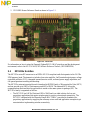
MC1321xEVK boards. The MC1321xEVK consists of the following two boards:
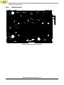
1. 13213-NCB Network Coordinator Board as shown in Figure 2-1.
Figure 2-1. 13213-NCB

System Overview
MC1321xEVK Reference Manual, Rev. 1.2
2-2 Freescale Semiconductor
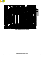
2. 13213-SRB Sensor Reference Board as shown in Figure 2-2.
Figure 2-2. 13213-SRB
For information on how to setup the Freescale Zigbee/802.15.4 MAC primitives and the development
environment, refer to the 802.15.4 MAC/PHY Software Reference Manual, (802154MPSRM).
2.1 MC1321x Solution
The MC1321x series RF transceiver is an IEEE
®
802.15.4-compliant radio that operates in the 2.4 GHz
ISM frequency band. The transceiver includes a low noise amplifier, 1mW nominal output power, voltage
controlled oscillator (VCO), integrated transmit/receive switch, on-board power supply regulation, and
full spread-spectrum encoding and decoding.
The MC1321x series microcontroller unit is based on the HCS08 Family of Microcontroller Units (MCU)
and can provide up to 60KB of flash memory and 4KB of RAM. The onboard MCU allows the
communications stack and also the application to reside on the same system-in-package (SiP). The
MC1321x family is organized as follows:
• The MC13211 has 16KB of flash and 1KB of RAM and is an ideal solution for low cost,
proprietary applications that require wireless point-to-point or star network connectivity. The
MC13211 combined with the Freescale Simple MAC (SMAC) provides the foundation for
proprietary applications by supplying the necessary source code and application examples to get
users started on implementing wireless connectivity.

System Overview
MC1321xEVK Reference Manual, Rev. 1.2
Freescale Semiconductor 2-3
• The MC13212 contains 32K of flash and 2KB of RAM and is intended for use with the Freescale
fully compliant 802.15.4 MAC. Custom networks based on the 802.15.4 standard MAC can be
implemented to fit user needs. The 802.15.4 standard supports star, mesh and cluster tree
topologies as well as beaconed networks.
• The MC13213 contains 60K of flash and 4KB of RAM and is also intended for use with the
Freescale fully compliant 802.15.4 MAC where larger memory is required.
The MC1321x includes two independent serial communications interface (SCI) modules. These serial
communications interfaces are connected to an RS-232 interface and a USB interface.
The MCU contains an analog to digital (ATD) converter module with 8 ports. A serial peripheral interface
(SPI) module handles the data communication between the MCU and the transceiver.
The MC1321x is housed in a 71-pin quad flat non-lead package (QFN). 9x9mm and is 1mm in height.
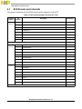
2.2 General-Purpose I/O and Peripheral Ports
Thirty eight pins are shared among general-purpose I/O (GPIO) and on-chip peripheral functions. The
MC1321x has six I/O ports, which include a total of up to 38 GPIO pins (one pin, PTG0, is output only).
Six of those pins are used internally on the IC, but it is available for debugging and monitoring.
The MCU provides control for the 802.15.4 modem. The required interconnects between the devices are
routed onboard the MC1321x SiP. In addition, the signals are brought out to external pads primarily for
use as test points. These signals can be useful when writing and debugging software.
Many of these pins are shared with on-chip peripherals such as timer systems, external interrupts, or
keyboard interrupts. When these other modules are not controlling the port pins, they revert to GPIO
control.
Immediately after reset, all 38 of these pins are configured as high-impedance general-purpose inputs with
internal pull-up devices disabled. The port allocation of the general-purpose I/O and on-chip peripheral
functions on the EVB are listed in Table 2-1.
Table 2-1. GPIO Port Allocation
Port 13213-NCB Functionality 13213-SRB Functionality
PTA0/KBD0 (UART) (MC1321x CTS)
PTA1/KBD1 (UART) (MC1321x RTS)
PTA2/KBD2 (Switch 1) (Switch 1)
PTA3/KBD3 (Switch 2) (Switch 2)
PTA4/KBD4 (Switch 3) (Switch 3)
PTA5/KBD5 (Switch 4) (Switch 4)
PTA6/KBD6 (USB to UART) (CP2102 CTS) (USB to UART) (CP2102 CTS)
PTA7/KBD7 (USB to UART) (CP2102 RTS) (USB to UART) (CP2102 RTS)

System Overview
MC1321xEVK Reference Manual, Rev. 1.2
2-4 Freescale Semiconductor
PTB0/AD0 LCD (LCD Enable) X-Y-Z Axis Accelerometer (G - Select
1)
PTB1/AD1 LCD (Register Select) X-Y-Z Axis Accelerometer (G - Select
2)
PTB2/AD2 LCD (Enable) X-Y-Z Axis Accelerometer (X-OUT)
PTB3/AD3 LCD (Data Read/Write) X-Y-Z Axis Accelerometer (Y-OUT)
PTB4/AD4 Data Line 4 X-Y-Z Axis Accelerometer (Z-OUT)
PTB5/AD5 Data Line 5 X-Y-Z Axis Accelerometer (Power
Save)
PTB6/AD6 Data Line 6 Vout (Temperature Sensor)
PTB7/AD7 Data Line 7 VCC (Temperature Sensor)
PTC0/TxD2 (USB to UART) (CP2102 RXD) (USB to UART) (CP2102 RXD)
PTC1/RxD2 (USB to UART) (CP2102 TXD) (USB to UART) (CP2102 TXD)
PTC2/SDA CS (EEPROM) CS (EEPROM)
PTC3/SCL Data (EEPROM) Data (EEPROM)
PTC4 (LED5) Green (LED5) Green
PTC5 CLK (EEPROM) CLK (EEPROM)
PTC6 Data (EEPROM) Data (EEPROM)
PTC7 (USB Suspend) (USB Suspend)
PTD0 ATTNB ATTNB
PTD1/RXTXEN RXTXEN RXTXEN
PTD2 (Buzzer) (Buzzer)
PTD3/RSTB RSTB RSTB
PTD4 (LED1) Red (LED1) Red
PTD5 (LED2) Red (LED2) Red
PTD6 (LED3) Red (LED3) Red
PTD7 (LED4) Red (LED4) Red
PTE0/TxD1 (UART) (MC1321x Tx)
PTE1/RxD1 (UART) (MC1321x Rx)
PTE2/CEB CEB CEB
PTE3/MISO MISO MISO
Table 2-1. GPIO Port Allocation
Port 13213-NCB Functionality 13213-SRB Functionality

System Overview
MC1321xEVK Reference Manual, Rev. 1.2
Freescale Semiconductor 2-5
For more details, see the MC1321x Datasheet, MC1321xDS.
2.3 Power-Saving Modes
The transceiver portion of the MC1321x uses the DOZE Mode as a power-saving mode. This mode greatly
reduces current consumption and has a typical current consumption of 40 µA. The SPI controls when the
transceiver enters and leaves DOZE mode on the MC1321x
The MCU portion of the MC1321x uses the STOP3 power-saving mode. The CPU, FLASH, and RAM are
in standby in the STOP3 mode. Also, all of the clocks in the MCU, including the oscillator itself, are halted.
Exiting the STOP3 mode is accomplished by the following:
• Asserting RESET
• An asynchronous interrupt pin (IRQ or KBI)
PTE4/MOSI MOSI MOSI
PTE5/SPICLK SPICLK SPICLK
PTE6 GPIO2 GPIO2
PTE7 GPIO1 GPIO1
PTG0/BKGD/MS (BDM) (BDM)
PTG1/XTAL
PTG2/EXTAL (CLKO) (CLKO)
Table 2-2. Pin Number to Signal Cross Reference
Pin Number MCU Signal Transceiver Signal
43 PTE6 GPIO2
44 PTE7 GPIO1
46 PTD0 ATTNB
65 PTE5_SPSCK SPICLK
66 PTE4_MOSI MOSI
67 PTE3_MISO MISO
68 PTE2_SS CEB
69 IRQ IRQB
70 PTD1 RXTXEN
71 PTD3 M_RSTB
Table 2-1. GPIO Port Allocation
Port 13213-NCB Functionality 13213-SRB Functionality

System Overview
MC1321xEVK Reference Manual, Rev. 1.2
2-6 Freescale Semiconductor
• Through the real-time interrupt
2.4 Clock
The MC1321x MCU contains an internal clock generation (ICG) module. An internal square wave clock
is fed from the MC1321x modem portion into the ICG module at the EXTAL pin on Port G. The clock
frequency is 62.5 KHz.
The MC1321x provides several options for the system clock configuration. The modem requires a 16MHz
crystal for its source oscillator and can also supply a selectable frequency clock out (CLKO). The CLKO
frequency can be programmed for the following:
• 16 MHz
•8 MHz
•4 MHz
•2 MHz
•1 MHz
• 62.5 kHz
• 32.786+ kHz (default)
• 16.393+ kHz
The MCU also has an internal clock generator that can be used for start-up and when the modem is
shutdown (for lowest power). The MCU internal reference is approximately 243 kHz.
2.5 Background Debug Module (BDM) Interface
A Background Debug Module (BDM) interface is available on the 13213-NCB and 13213-SRB. The
BDM interfaces to the MCU provide an interface for programming the on-chip FLASH. The BDM
connector provides the ability to connect a debug interface for development and for accessing different
memory data.
The BDM interface can also be used for traditional debugging. Debugging is accomplished using the
CodeWarrior IDE for HCS08.
2.6 Reset
The RESET is a dedicated pin with a built-in pull-up device. This pin is connected to the 6-pin BDM
connector to allow a development system to directly reset the MCU. The MCU resets the 13213-NCB and
13213-SRB as part of its startup sequence when power is applied and the On/Off switch is turned on. If
required, a manual external reset can be executed by pressing the reset switch. In all cases, the reset
sequence resets the MCU, which in turn, resets the transceiver.

MC1321xEVK Reference Manual, Rev. 1.2
Freescale Semiconductor 3-1
Chapter 3
RF Front End
This chapter provides a description of the external analog circuitry required to ensure correct operation of
the MC1321x solution. This section primarily refers to the RF section of the MC1321x solution.
3.1 RF Transceiver
The MC1321x contains an RF transceiver which is an 802.15.4 Standard-compliant radio that operates in
the 2.4 GHz ISM frequency band. The transceiver includes a low noise amplifier, 1mW nominal output
power, PA with internal voltage controlled oscillator (VCO), integrated transmit/receive switch, on-board
power supply regulation, and full spread-spectrum encoding and decoding.
The RF interface allows both single port differential operation and dual port differential operation.
See the MC132x Reference Manual (MC1321xRM) for more details.
3.1.1 DC Biasing
To ensure correct operation, the inputs and outputs should have the following bias:
• RX inputs: Grounded.
• TX outputs: Connected to VDDA
The DC bias path is through the baluns and matching network. The external switch is supplied from
GPIO1, which is high in RF active mode. The output switches between RX and TX. This output is 1.8V
only.
NOTE
If the full - 40 to 85° C temperature range is required, a buffer should be
inserted to raise this control pin to the battery supply. At -40° C, 1.8 V may
not be enough to correctly toggle the switch.
3.2 RF Matching
The differential output impedance of the MC1321x is approximately 300-450 ohms and 0.6 pF in parallel.
The impedance is slightly different between RX and TX.
An LC-matching network steps the impedance down to 50 Ohms balanced and a small ceramic balun
allows the differential to single-ended transformation. A 50:50 ohm balun is used.
Although the component values are slightly different for RX and TX to accommodate the different
impedances, the overall function is the same. The low-pass LC network configuration reduces TX
harmonics.

RF Front End
MC1321xEVK Reference Manual, Rev. 1.2
3-2 Freescale Semiconductor
The center tap on the balun provides DC ground for the RX input pins and biases the TX output pins to
VDDA. The TX balun is RF decoupled.
By moving a 0 ohm jumper, it is possible to select between an on-board F-antenna or an SMA connector
for easy RF evaluation and/or for using an external antenna.
3.3 On-board Antenna
For ease of use, a PCB F-antenna resides on the board. The antenna bandwidth measured an approximate
–10 dB return loss point at approximately 350 MHz. The resonant frequency is 2.44 GHz.
Mounting the board in a kit box causes the antenna resonant frequency to shift slightly down in frequency,
but due to the high bandwith, this does not have any functional effects.
• Return loss across the ISM band is better than –15 dB
• The radiation pattern is omnidirectional and is very efficient
• The antenna is enabled (default)
For RF measurements or for evaluating other antennas, connector J100 (SMA) can be enabled by moving
a 0 Ohm jumper.
3.4 Internal Power Supplies
The MC1321x has built in voltage regulators for the internal RF circuits (1.8V nominal). RF performance
is not affected by varying supply voltage and the regulators provide some noise suppression allowing less
stringent supply requirements.
3.4.1 RF Section
Input is VBATT and VDDINT. The recommended operating range is 2.0-3.4V (3.6V absolute maximum).
This should be decoupled with 1 uF capacitor or more.
The three outputs (VDDA + VDDLO1 + VDDLO2, VDDD and VDDVCO) should each be decoupled
with 100 nF capacitor to ensure stability and low noise. The value is not critical.
3.4.2 Digital Section
Input is VDD and VDDAD. Recommended decoupling is 100 nF on each input.
The Operating range is 2.05 –3.4V with 3.4V being the absolute maximum.
3.5 Reference Oscillator
The MC1321x reference oscillator is a very low power oscillator to save battery consumption in Sleep and
Doze Modes.
The current consumption is controlled by software. The default value is 12 µA. In Doze Mode, it is
possible to lower the current to 6 µA, but this sets tighter requirements on the XTAL to ensure oscillation.

RF Front End
MC1321xEVK Reference Manual, Rev. 1.2
Freescale Semiconductor 3-3
The Reference frequency is 16.000 MHz only. CLK0 supplies the MCU with a clock.
To fulfill the 802.15.4 Standard requirements, the reference frequency must be within ± 40 ppm of
nominal. This includes the following:
• Initial tolerance
• Aging
• Crystal temperature drift
• Spread on the external loading capacitors
The MC1321x has a built-in trimming facility that allows the initial tolerance to be calibrated out during
production.
See AN3251, Reference Oscillator Crystal Requirements for the MC1319x, MC1320x and MC13221x.
3.6 RF Performance
The following performance has been measured on the 13213-NCB and 13213-SRB boards as referenced
to the SMA connector. Stated typical measured values and spread represents actual measurements on 10
boards, indicating the performance that can be expected. These values does not represent guaranteed
performance.
3.6.1 TX Power
The output power is software adjustable with a tuning range of more than 20 dB.
The default power setting (Register 12: BC) is -1 dBm. This is a slight compromise between output power
and current consumption. The obtainable maximum output power is 3 dBm. This setting assumes a higher
current consumption can be tolerated.
Tolerance: ±1 dBm
The 802.15.4 Standard requirement is greater than -3 dBm.
3.6.2 Harmonics
2nd harmonic is typically -40 dBm or lower.
3rd harmonic is low, but does not exceed -45 dBm.
The 802.15.4 Standard requirement is less than -30 dBm
3.6.3 RX Sensitivity
Sensitivity was measured at -95 dBm, ±2 dBm (1% PER, 20 byte payload).
The 802.15.4 Standard requirement is less than -85 dBm.

RF Front End
MC1321xEVK Reference Manual, Rev. 1.2
3-4 Freescale Semiconductor
Page is loading ...
Page is loading ...
Page is loading ...
Page is loading ...
Page is loading ...
Page is loading ...
Page is loading ...
Page is loading ...
Page is loading ...
Page is loading ...
Page is loading ...
Page is loading ...
Page is loading ...
Page is loading ...
Page is loading ...
Page is loading ...
Page is loading ...
Page is loading ...
-
 1
1
-
 2
2
-
 3
3
-
 4
4
-
 5
5
-
 6
6
-
 7
7
-
 8
8
-
 9
9
-
 10
10
-
 11
11
-
 12
12
-
 13
13
-
 14
14
-
 15
15
-
 16
16
-
 17
17
-
 18
18
-
 19
19
-
 20
20
-
 21
21
-
 22
22
-
 23
23
-
 24
24
-
 25
25
-
 26
26
-
 27
27
-
 28
28
-
 29
29
-
 30
30
-
 31
31
-
 32
32
-
 33
33
-
 34
34
-
 35
35
-
 36
36
-
 37
37
-
 38
38


Ask a question and I''ll find the answer in the document
Finding information in a document is now easier with AI
Related papers
Other documents
-
Freescale Semiconductor DEMO9S08AC60E User manual
-
Emtec EKMMD32GS100 Datasheet
-
-
Marshall Electronics NCB-2010 Operating Instructions Manual
-
Silicon Labs CP2102 Evaluation Kit User guide
-
-
 intwine connect ICG-150 User guide
-
DFROBOT DFR0603 User manual
-
-
MOBILICOM MCU-30 User manual
