Page is loading ...

© Semiconductor Components Industries, LLC, 2020
July, 2020 − Rev. 0 1Publication Order Number:
EVBUM2748/D
SECO-NCD57000-GEVB
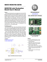
NCD57000 mini Evaluation
Board User's Manual
Purpose
This document describes the use and applications for the
NCD57000 gate driver mini board. The board is designed on a two
layer PCB and includes the NCD57000 driver and all the necessary
drive circuitry. The board also includes ability to solder any MOSFET
or SiC MOSFET in a TO−247 high voltage package and compatibility
with SECO−GDBB−GEVB baseboard for out−of−the−box evaluation.
The board does not include a power stage and is generic from the point
of view that it is not optimized to any particular topology. It can be
used in any low−side or high−side power switching application. For
bridge configurations two or more of these boards can be configured in
a totem pole type drive configuration. The boards can be considered as
an isolator+driver+TO−247 discrete module.
NCD57000 Description
NCD57000 is a high−current single channel IGBT driver with
internal galvanic isolation, designed for high system efficiency and
reliability in high power applications. Its features include
complementary inputs, open drain FAULT and Ready outputs, active
Miller clamp, accurate UVLOs, DESAT protection, soft turn−off at
DESAT, and separate high and low (OUTH and OUTL) driver outputs
for system design convenience. NCD57000 accommodates both 5 V
and 3.3 V signals on the input side and wide bias voltage range on the
driver side including negative voltage capability. NCD57000 provides
> 5 kVrms (UL1577 rating) galvanic isolation and > 1200 Viorm
(working voltage) capabilities. NCD57000 is available in the
wide−body SOIC−16 package with guaranteed 8 mm creepage
distance between input and output to fulfill reinforced safety
insulation requirements.
Collaterals
•SECO−NCD57000−GEVB
•SECO−GDBB−GEVB
•NCD57000
Figure 3. Schematic
www.onsemi.com
EVAL BOARD USER’S MANUA
L
Figure 1. SECO−NCD57000−GEVB
Figure 2. Board Plugged into
SECO−GDBB−EVB
F
eatures
•Galvanic Isolated Gate Driver Circuit 5 kV
•Demonstrates NCD57000 Isolated Driver
with Advanced Features
•Replaceable Load Capacitor and Gate
Resistor for different Load Simulation
•Plug−and−Play Testing with
SECO−GDBB−GEVB
•Minimized Form−factor for Embedding an
d
Testing in Application Boards or New
Designs
•Custom Voltage Levels with External
Power Supply

SECO−NCD57000−GEVB
www.onsemi.com
3
Figure 7. SECO−GDBB−GEVB
Table 1. NCD57000 mini BOARD BOM
Description
Designa-
tor
Quantity
Value
Comment
Footprint
Manufacturer
Capacitor 0805 1
m
F 50 V
C1, C3, C5
3
1
m
F
CAP0805
TDK
Capacitor 0805 100 nF 50 V
C2, C4, C7
3
100 nF
CAP0603
Kyocera AVX
Capacitor 0805 10 pF 50 V
C6
1
10 pF
CAP0603
KEMET
BYG23T−M3/TR
D1
1
SMB
Vishay
Semiconductor
Schottky Diode
D2, D3
2
MBR0540
SOD−123
ON Semiconductor
NCD57000
IC1
1
DSO−16_N
ON Semiconductor
Header, 7−Pin
P1
1
Don’t assembly
HDR1X7
Molex
Header, 3−Pin
P2
1
Don’t assembly
HDR1X3
Molex
RES SMD 10 k
W
1% 1/10W 0603
R1, R2,
R3, R4, R5
5
10k
RES0603
Yageo
RES SMD 1 k
W
1% 1/10W 0603
R5
1
1k
RES0603
Bourns
RES SMD 4.7
W
1% 1/10W 0805
RGH1,
RGL1
2
4.7R
RES0805
Yageo

SECO−NCD57000−GEVB
www.onsemi.com
4
PCB Assembly and Layers
Figure 8 and Figure 9 shows the top and bottom layouts of
the PCB. The PCB is 35 mm x 18 mm x 1 mm (length x width x height) where the width of the PCB is approximately the
width of a TO*247 body.
Figure 8. NCD57000 mini Board TOP Assembly Drawing
Figure 9. NCD57000 mini Board BOTTOM Assembly Drawing
I/O Connectors
There are 3 I/O connectors including 13 pins described in
Table 2 below. The signals on low voltage side are noted as
“primary” ground referenced. There is no true “primary”
and “secondary” ground but there is 1.2 kV galvanic
isolation across the isolation boundary. It is especially
important to maintain isolation in high−side, high−voltage,
switching applications where the “secondary” Vcc (P3.2
and P3.3) floats Vcc volts above the power supply input
voltage:
Table 2. I/O CONNECTOR DESCRIPTIONS
Ref Des
Name
I/O
GND Ref
Description
Value [V]
P1.1
Vcc1
Power
Primary
Positive primary power supply
5
P1.2
Gnd1
Power
Primary
Ground
0
P1.3
IN+
Input
Primary
Non−inverting PWM input
0 − 3.3 (5)
P1.4
FLT
Output
Primary
Fault flag
0 − 5 (3.3)
P1.5
IN−
Input
Primary
Inverting PWM input
0 − 5 (3.3)
P1.6
RDY
Output
Primary
Ground
0 − 5 (3.3)
P1.7
RST
Input
Primary
Reset FLT pin
0 − 5 (3.3)
P2.1
Vcc2
Power
Secondary
Positive branch power supply
< 20
P2.2
Gnd2
Power
Secondary
Ground of the power supply
0
P2.3
Vee2
Power
Secondary
Negative branch of power supply
> −10
G (G)
Gate
Output
Secondary
Gate pin of a power switch
< 20
C (D)
Collector
Output
Secondary
Collector (drain) pin of a power switch
≤
1200
E (S)
Emitter
Output
Secondary
Emitter (source) pin of a power switch
0

SECO−NCD57000−GEVB
www.onsemi.com
5
Mounting into Existing PCB
The board can be mounted into an existing power board,
shown as “Main PCB” in Figure 6. If there are no
components or low profile surface mount components only,
the mini SMD EVB can be mounted parallel to the main
PCB as shown in Figure 6. The TO−247, power device leads
would pass through the mini EVB plated thru−holes and into
the main PCB. Or, if necessary, the gate lead of the TO−247,
power device can be soldered to the plated thru−hole on the
EVB and cut so that it does not contact the main PCB. For
mechanical strength, it is preferred that the TO−247 gate
lead pass through both PCB’s. This configuration is helpful
for already existing application with horizontal TO−247
positions.
Recommended procedure for Option 1 Mounting into an
existing PCB:
1. On the main PCB, isolate the gate drive to the
TO−247. If the existing design includes a gate
drive resistor, removing it should serve the
purpose of isolating the gate drive to the TO−247.
If there is no series component between the PWM
signal source and the TO−247 gate lead, the gate
drive PCB track will need to be cut.
2. Measure the resistance between the PWM source
and the TO−247 gate lead (or PWM source to gate
drive transformer/isolator if applicable). Verify
reading is high impedance (open).
3. If a TO−247 discrete is installed in the main PCB,
remove it now.
4. Place Kapton or non−conductive tape over the
main PCB area directly beneath the EVB.
This is to avoid the possibility of having any
components on the bottom of the mini SMD EVB
touch components or conductive surfaces on the
main PCB.
5. Solder a flying lead of bus wire to the main PCB,
PWM signal and so on. Make sure there is enough
length of the PWM input (flying lead) to reach
through the EVB.
6. Solder the TO−247 through just the EVB first
7. With the TO−247 installed into the EVB, install
and solder the TO−247 leads into the main PCB.
8. Solder the other end of the PWM input (flying
lead) to IN+ for non−inverting PWM applications
or IN− for inverting PWM applications.
9. Using the same size bus wire, solder the remaining
connections between the EVB to the appropriate
locations on the main PCB.
10. Solder flying leads for bias voltage. Note that P2
are across the isolation boundary from.
Mounting into Existing PCB − Option 2
If components mounted on the main PCB interfere with
mounting the EVB as described by Option 1 (Figure 10), the
TO−247 leads can be formed (lead length may need to be
added) with the EVB mounted perpendicular to the main
PCB as shown in Figure 11. If required, both mounting
options allow the application of a heat sink to the TO−247
package. If high dv/dt is present on the drain of the TO−247,
the EVB should be angled, away from being parallel to the
TO−247, as much as possible.
1. On the main PCB, isolate the gate drive to the
TO−247 power device. If the existing design
includes a gate drive resistor, removing it should
serve the purpose of isolating the gate drive to the
TO−247. If there is no series component between
the PWM signal source and the TO−247 gate lead,
the gate drive PCB track will need to be cut.
2. Measure the resistance between the PWM source
and the TO−247 gate lead (or PWM source to gate
drive transformer/isolator if applicable). Verify
reading is high impedance (open).
3. If a TO−247 discrete is installed in the main PCB,
remove it now.
4. Solder a flying lead of bus wire to the main PCB,
PWM signal. Make sure there is enough length of
the PWM input (flying lead) to reach through the
mini EVB plated thru−hole.
5. After the TO−247 leads have been formed, check
for fit through the EVB and down into the main
PCB
6. Solder the TO−247 through just the EVB first
7. With the TO−247 installed into the EVB, install
and solder the TO−247 leads into the main PCB
8. Solder the other end of the PWM input (flying
lead) to IN+ for non−inverting PWM applications
or IN− for inverting PWM applications.
9. Using the same size bus wire, solder the remaining
connections between EVB to the appropriate
locations on the main PCB.
10. Solder flying leads from bias voltage to the EVB.
Note that power supply connector is across the
isolation boundary.

SECO−NCD57000−GEVB
www.onsemi.com
6
Figure 10. Mounting into Existing PCB
Low voltage
signals
Low voltage
signals
TO247 TO247
Main PCB
Secondary
power supply
Secondary
power supply
Signals and/or power supply can be
soldered from topside
Signals and/or power supply canbe
soldered from topside
Figure 11. EVB Board Installations
Main PCB
Heatsink
Heatsink
TO247
TO247
EVB board
EVB board
Mounting into New PCB Design
The EVB can also be used as an isolator+driver+TO−247
“driver module” that can be integrated into a new PCB
design. The gate lead of the TO−247 between the EVB and
the main PCB is for mechanical strength only. For main PCB
layout, the gate lead extends down through the main PCB
and can be soldered to an isolated plated thru−hole. As
shown in Figure 12, shoulder pins with appropriate flange
are one option that can be used as mounting pins between
mini EVB and the main PCB. In the case new design
Figure 13 all needed for footprint design.
Figure 12. NCD57000 SMD mini Board New Design Installations
Main PCB
TO 247
Power supply
Interface
TO247
Power supply
Interface
Heatsink
Heatsink

SECO−NCD57000−GEVB
www.onsemi.com
7
Figure 13. EVB’s PCB Mechanical Data
Testing without Installing into a PCB
The EVB can also be tested without installing into a main
PCB. However, since this EVB was designed for small form
factor there are no test points included for connecting
voltage probes. The EVB should be hand probed carefully
since the components are very fine pitch or flying leads
connected to desired probe points can be attached. The
20 Vdc bias (Vcc2 and Gnd2) is on the secondary side of the
isolated gate driver IC and therefore has a separate/isolated
return ground from the 5 Vdc bias (Vcc1 and Gnd2). The
recommended series load of below 4.7 nF and 4.7 W is close
to what might be representative of a power switch gate drive
input impedance. Leaded passive components can be
soldered into the TO−247 holes as shown in Figure 14.
Alternatively, a TO−247 power switch can also be soldered
in place and used as a load for the gate driver board. Note that
testing without installing into a power stage, leaves the
DESAT pin open since there is no active drain signal. The
effect of operating DESAT this way is explained in section
‘DESAT’.
Testing with Gate Driver Base Board
Another very easy way how to test and evaluate more mini
boards at same time is to use dedicated base board
containing all necessary for easy use. Figure 15 shows
typical example where we only need scope for detail
waveform analyzing and precise measurement. The base
board makes possible connect up to 200 V voltage for power
device loading to see impact of non−linear miller capacity to
driving performance.

SECO−NCD57000−GEVB
www.onsemi.com
9
DESAT Setup
DESAT is a type of short circuit or/and over−current
protection dedicated to monitoring the ID·RDS of the
MOSFET or Vce_sat voltage for bipolar device like IGBTs.
The EVB is preconfigured with R5 = 1 kW (DESAT
resistor). The internal DESAT threshold is fixed at
VDESAT(TH) = 9 V and the DESAT signal amplitude is
adjustable by R5 and HV diode connected in series with R5.
R5 = 1 kW may not be the correct resistor value for some
applications. If VDESAT > 9 V during normal operation,
decrease R5 to lower the signal amplitude. If DESAT is
active, the output is driven low. Further, the /FLT output is
activated, please refer to datasheet for more details.
Basic Measurement
Figure 16 and Figure 17 show basic gate driver board
connected to base board according the Figure 15. Very easily
can be evaluated time delays, maximal gate current
capability or maximal switch frequency before thermal
runaway at given condition and similar. Typically we can
measure time between fault event and FLT pin reaction.
Typical task is to compare different part number at same
time and/or same condition to see online all, for application,
important behaviors.
Figure 16. Normal Operation for Turn−on and Turn−off
IN+
Ig
VG
Figure 17. Zoom of Normal Operation for Turn−on and Turn−off
IN+
Ig
VG

www.onsemi.com
1
ON Semiconductor and the ON Semiconductor logo are trademarks of Semiconductor Components Industries, LLC dba ON Semiconductor or its subsidiaries in the United States and/or
other countries. ON Semiconductor owns the rights to a number of patents, trademarks, copyrights, trade secrets, and other intellectual property. A listing of ON Semiconductor’s
product/patent coverage may be accessed at www.onsemi.com/site/pdf/Patent−Marking.pdf. ON Semiconductor is an Equal Opportunity/Affirmative Action Employer. This literature is
subject to all applicable copyright laws and is not for resale in any manner.
The evaluation board/kit (research and development board/kit) (hereinafter the “board”) is not a finished product and is as such not available for sale to consumers. The board is only intended
for research, development, demonstration and evaluation purposes and should as such only be used in laboratory/development areas by persons with an engineering/technical training
and familiar with the risks associated with handling electrical/mechanical components, systems and subsystems. This person assumes full responsibility/liability for proper and safe handling.
Any other use, resale or redistribution for any other purpose is strictly prohibited.
The board is delivered “AS IS” and without warranty of any kind including, but not limited to, that the board is production−worthy, that the functions contained in the board will meet your
requirements, or that the operation of the board will be uninterrupted or error free. ON Semiconductor expressly disclaims all warranties, express, implied or otherwise, including without
limitation, warranties of fitness for a particular purpose and non−infringement of intellectual property rights.
ON Semiconductor reserves the right to make changes without further notice to any board.
You are responsible for determining whether the board will be suitable for your intended use or application or will achieve your intended results. Prior to using or distributing any systems
that have been evaluated, designed or tested using the board, you agree to test and validate your design to confirm the functionality for your application. Any technical, applications or design
information or advice, quality characterization, reliability data or other services provided by ON Semiconductor shall not constitute any representation or warranty by ON Semiconductor,
and no additional obligations or liabilities shall arise from ON Semiconductor having provided such information or services.
The boards are not designed, intended, or authorized for use in life support systems, or any FDA Class 3 medical devices or medical devices with a similar or equivalent classification in
a foreign jurisdiction, or any devices intended for implantation in the human body. Should you purchase or use the board for any such unintended or unauthorized application, you shall
indemnify and hold ON Semiconductor and its officers, employees, subsidiaries, affiliates, and distributors harmless against all claims, costs, damages, and expenses, and reasonable
attorney fees arising out of, directly or indirectly, any claim of personal injury or death associated with such unintended or unauthorized use, even if such claim alleges that ON Semiconductor
was negligent regarding the design or manufacture of the board.
This evaluation board/kit does not fall within the scope of the European Union directives regarding electromagnetic compatibility, restricted substances (RoHS), recycling (WEEE), FCC,
CE or UL, and may not meet the technical requirements of these or other related directives.
FCC WARNING – This evaluation board/kit is intended for use for engineering development, demonstration, or evaluation purposes only and is not considered by ON Semiconductor to
be a finished end product fit for general consumer use. It may generate, use, or radiate radio frequency energy and has not been tested for compliance with the limits of computing devices
pursuant to part 15 of FCC rules, which are designed to provide reasonable protection against radio frequency interference. Operation of this equipment may cause interference with radio
communications, in which case the user shall be responsible, at its expense, to take whatever measures may be required to correct this interference.
ON Semiconductor does not convey any license under its patent rights nor the rights of others.
LIMITATIONS OF LIABILITY: ON Semiconductor shall not be liable for any special, consequential, incidental, indirect or punitive damages, including, but not limited to the costs of
requalification, delay, loss of profits or goodwill, arising out of or in connection with the board, even if ON Semiconductor is advised of the possibility of such damages. In no event shall
ON Semiconductor’s aggregate liability from any obligation arising out of or in connection with the board, under any theory of liability, exceed the purchase price paid for the board, if any.
For more information and documentation, please visit www.onsemi.com.
PUBLICATION ORDERING INFORMATION
TECHNICAL SUPPORT
North American Technical Support:
Voice Mail: 1 800−282−9855 Toll Free USA/Canada
Phone: 011 421 33 790 2910
LITERATURE FULFILLMENT:
Email Requests to: [email protected]
ON Semiconductor Website: www.onsemi.com
Europe, Middle East and Africa Technical Support:
Phone: 00421 33 790 2910
For additional information, please contact your local Sales Representative
◊
/


