
UM10402
STARplug Triple Output demo board
Rev. 1 — 1 September 2011 User manual
Document information
Info Content
Keywords STARplug, SMPS, flyback, converter
Abstract The NXP Semiconductors STARplug Triple Output demo board comes in
two versions: 12 W and 18 W. By default the boards are configured as an
isolated SMPS with DC output voltages at 12 V, 5 V and 3.3 V. Multiple
configurable options are available on these boards; for example: snubber
type, regulation and feedback strategy and more. The boards use the
TEA1523P SMPS IC in a DIP8 package.
This manual describes the STARplug Triple Output demo board version
1.10.
Refer to the TEA152x data sheet for details on the STARplug device and
the STARplug application note AN00055 for general application
information.

UM10402 All information provided in this document is subject to legal disclaimers. © NXP B.V. 2011. All rights reserved.
User manual Rev. 1 — 1 September 2011 2 of 24
Contact information
For more information, please visit: http://www.nxp.com
For sales office addresses, please send an email to: [email protected]
NXP Semiconductors
UM10402
STARplug Triple Output demo board
Revision history
Rev Date Description
v.1 20110901 first issue

UM10402 All information provided in this document is subject to legal disclaimers. © NXP B.V. 2011. All rights reserved.
User manual Rev. 1 — 1 September 2011 3 of 24
NXP Semiconductors
UM10402
STARplug Triple Output demo board
1. Introduction
The STARplug Triple Output SMPS demo board described in this user manual produces
DC output voltage levels at 12 V, 5 V and 3.3 V. The 5 V and 3.3 V outputs are generated
by separate flyback transformer taps of the 12 V secondary winding. The board has a
universal mains input and the total nominal output power is rated at either 12 W or 18 W
depending on the version.
The flyback circuit is built around the NXP Semiconductors TEA1523P STARplug IC. On
the STARplug Triple Output demo board several provisions are available enabling
modification of the input filtering, snubber circuit, regulation feedback scheme and output
filtering. Small changes in output voltage (up to 20 %) are also supported but the ratio
between the three output voltages remains unaltered. If an alternative transformer is
considered, the PCB can be used to generate virtually any output voltage and output
voltage combination.
These features make the STARplug Triple Output demo board very versatile but this
versatility requires some Printed-Circuit Board (PCB) space. Therefore, this board is not
intended as a showcase for minimal PCB space utilization. The demo board is intended
for exploring the features/possibilities of the STARplug family of ICs. It is ideal for use in
both the design and development phases of a final solution for multi-output low power
Switched Mode Power Supply (SMPS).
1.1 Features
• Universal mains input
• DC output voltages: 12 V, 5 V and 3.3 V
• Stable regulated voltage
• Highly flexible and easily tuned to meet user requirements
• Used with the TEA1523P
• 12 W or 18 W nominal output power; board version dependent
• Highly efficient: > 80 %
• Low standby (no-load) power: < 80 mW
• OverPower Protection (OPP)
• OverTemperature Protection (OTP)
• Built-in ElectroMagnetic Interference (EMI) filter
WARNING
Lethal voltage and fire ignition hazard
The non-insulated high voltages that are present when operating this product, constitute a
risk of electric shock, personal injury, death and/or ignition of fire.
This product is intended for evaluation purposes only. It shall be operated in a designated test
area by personnel qualified according to local requirements and labor laws to work with
non-insulated mains voltages and high-voltage circuits. This product shall never be operated
unattended.

UM10402 All information provided in this document is subject to legal disclaimers. © NXP B.V. 2011. All rights reserved.
User manual Rev. 1 — 1 September 2011 4 of 24
NXP Semiconductors
UM10402
STARplug Triple Output demo board
2. Technical specification
Remark: Output voltages 2 and 3 can vary considerably when no-load is connected
because this output voltage is not regulated in the default configuration.
3. Performance data
3.1 Output voltage and no-load power consumption
Table 3 shows the no-load power consumption figures for the STARplug Triple Output
demo board’s default configuration.
Remark: Output voltages 2 and 3 can vary considerably when no-load is connected
because this output voltage is not regulated in the default configuration.
Table 1. Input specification
Parameter Condition Value Remark
Input voltage (V
i
)- 90V(AC) to
276 V (AC)
universal mains
Input frequency (f) - 47 Hz to 63 Hz -
Table 2. Output specification
Output supply Condition Value Remark
Output voltage 1 - 12 V default configuration: regulated output
Output voltage 1 tolerance at 75 % load 2% -
Output voltage 1 stability - 2 % Over full power range
Output voltage 2 - 5 V default configuration: non-regulated
Output voltage 2 tolerance - - dependent on the load on output 1
Output voltage 2 stability - - dependent on the load on output 1
Output voltage 3 - 3.3 V default configuration: non-regulated
Output voltage 3 tolerance - - dependent on the load on output 1
Output voltage 3 stability - - dependent on the load on output 1
Table 3. No-load output voltage and power consumption
Condition Energy start 2.0
requirement
Output voltage 1 Power consumption
12 W version
115V/60Hz 300 mW 11.9 V 75 mW
230 V/50 Hz 300 mW 11.9 V 75 mW
18 W version
115V/60Hz 300 mW 11.9 V 77 mW
230 V/50 Hz 300 mW 11.9 V 77 mW

UM10402 All information provided in this document is subject to legal disclaimers. © NXP B.V. 2011. All rights reserved.
User manual Rev. 1 — 1 September 2011 5 of 24
NXP Semiconductors
UM10402
STARplug Triple Output demo board
3.2 Efficiency performance data
Table 4 shows the efficiency figures for the default configuration of the STARplug Triple
Output demo board.
Remark: The load is on the 12 V output only.
Remark: The warm-up time is 15 minutes and the settle time, after load change, is 90 s.
3.3 ElectroMagnetic Compatibility (EMC) performance data
Table 4. Efficiency of the 12 W version
Power
supply
Energy star
requirement
Efficiency ()
average 25 % load 50 % load 75 % load 100 % load
12 W version
115 V/ 60 Hz 77.8 % 80.7 % 81.3 % 81.3 % 80.8 % 79.2 %
230 V/ 50 Hz 77.8 % 80.9 % 79.4 % 81.4 % 81.8 % 81.0 %
18 W version
115 V/ 60 Hz 80.3 % 81.9 % 82.9 % 83.4 % 81.1 % 80.1 %
230 V/ 50 Hz 80.3 % 82.0 % 81.2 % 82.4 % 82.3 % 82.2 %
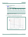
Fig 1. Conducted EMC tests - V
IN
= 115 V (AC), P
o
= 12 W
019aab907

UM10402 All information provided in this document is subject to legal disclaimers. © NXP B.V. 2011. All rights reserved.
User manual Rev. 1 — 1 September 2011 6 of 24
NXP Semiconductors
UM10402
STARplug Triple Output demo board
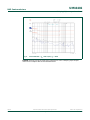
Fig 2. Conducted EMC - V
IN
= 230 V (AC), P
o
= 12 W
Fig 3. Conducted EMC - V
IN
= 115 V (AC), P
o
= 18 W
019aab908
019aab909

UM10402 All information provided in this document is subject to legal disclaimers. © NXP B.V. 2011. All rights reserved.
User manual Rev. 1 — 1 September 2011 7 of 24
NXP Semiconductors
UM10402
STARplug Triple Output demo board
Remark: Average and quasi-peak EMC performance of the STARplug Triple Output
demo board complies with the standard EN55022.
Fig 4. Conducted EMC - V
IN
= 230 V (AC), P
o
= 18 W
019aab910

UM10402 All information provided in this document is subject to legal disclaimers. © NXP B.V. 2011. All rights reserved.
User manual Rev. 1 — 1 September 2011 8 of 24
NXP Semiconductors
UM10402
STARplug Triple Output demo board
4. Connections of the demo board
Remark: Reversing the live (J2) and neutral (J1) connections has no influence on the
operation of the STARplug Triple Output demo board. Terminal J3 produces 12 V, J4
produces 5 V and J5 produces 3.3 V. Terminal J6 is the reference (GND, 0 V) secondary
side reference terminal.
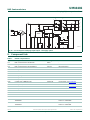
5. Circuit description
The default STARplug Triple Output SMPS demo board consists of a single-phase full
wave rectifier circuit, a filtering section, a switching section, an output section and a
feedback section. The full circuit diagram of the default configuration of the STARplug
Triple Output demo board PCB is shown in Figure 6
. Secondary side feedback and
regulation are implemented on the 12 V output only.
5.1 Rectification section
The single-phase full wave rectifier is built around a standard Graetz bridge rectifier
component (BR1). Capacitors C3 and C4 function as reservoir capacitors for the rectified
input voltage. Resistor R1 limits the inrush current. Resistor R1 must be a carbon resistor,
not a metal film resistor. A metal film resistor could work as a fuse instead of an inrush
current limiter.
Terminals J1 and J2 connect the input to the electricity utility network. J1 is referred to as
neutral and J2 as live for convenience. Swapping these two wires does have no effect on
the actual operation of the STARplug Triple Output converter.
Fig 5. Demo board connections setup
019aab911
Live (J2)
Neutral (J1)
(J3) 12 V
(J4) 5 V
(J5) 3.3 V
(J6) 0 V

UM10402 All information provided in this document is subject to legal disclaimers. © NXP B.V. 2011. All rights reserved.
User manual Rev. 1 — 1 September 2011 9 of 24
NXP Semiconductors
UM10402
STARplug Triple Output demo board
5.2 Filtering section
The filtering section consists of the common mode choke L1/C1 on the AC-side of the
diode bridge and C3, L2, C4 in -configuration on the DC-side. The whole filtering
configuration effectively reduces the noise and harmonic content that is otherwise injected
from the TEA1523 switching electronics into the electricity utility network. The circuitry
helps to achieve the EMC performance required by the standard EN55022.
5.3 Switching section
The switching section uses the NXP Semiconductors STARplug TEA1523 IC in a DIP8
package. The operating frequency is set using the combination of R2 and C4. The parallel
circuit of resistors R3/R3A, limit the peak current that can occur in the STARplug internal
MOSFET switch and consequently in the Transformer T1 primary winding. Current
limitation prevents the internal MOSFET switch from being overstressed (the maximum
switch current is given in Equation 1
). In addition, it acts as an overload protection for the
SMSP output.
(1)
The auxiliary winding on transformer T1 generates the supply voltage for the TEA1523 IC.
The voltage from the auxiliary winding is (half-wave) rectified by diode D2 and capacitor
C5 is charged. Resistor R9 limits the current. The voltage on C5 is the supply voltage for
the TEA1523 VCC pin.
The IC’s AUX pin receives voltage information regarding the magnetization status of
transformer T1 through resistor R5.
A snubber circuit manages the voltage spikes and associated energy (due to the leakage
inductance of the primary winding of transformer T1). It is implemented using a
diode-Zener snubber (D3 and D4). This type of snubber conserves energy and is EMI
friendly but it is a more expensive option when compared to RCD snubbers (see
Section 6.1
).
5.4 Output section
The output section of the STARplug Triple Output application produces 3 DC voltages:
12 V, 5 V and 3.3 V.
The 12 V section consists of diode D5, capacitors C12, C13, C16, and inductor L5. Spikes
on the output above 13 V are clamped by Zener diode D10. Similar configurations are
implemented for the 5 V and 3.3 V output sections. The output sections provide a good
level of ripple filtering and noise suppression by using -configurations in all output
sections.
All output voltages are generated using the potential at J6 (GND; 0 V) as reference. J3
produces 12 V, J4 produces 5 V and J3 produces 3. 3 V.
I
DS max
0.5
R3//R3A
----------------------
=

UM10402 All information provided in this document is subject to legal disclaimers. © NXP B.V. 2011. All rights reserved.
User manual Rev. 1 — 1 September 2011 10 of 24
NXP Semiconductors
UM10402
STARplug Triple Output demo board
5.5 Feedback section
The feedback signal is taken from the 12 V supply through resistor R20. The user can
change that to one of the other output voltages or a weighed combination thereof (see
Section 6.4
). In the default configuration, the feedback network on the secondary side
consists of R13, R14, R20, C18, C19 and voltage reference IC3 (a TL431A). Resistors
R20 and R14 form a voltage divider and determine the output voltage of the (12 V) supply.
The programmed output voltage (of the 12 V output - terminal J3) is calculated using
Equation 2
(2)
The factor V
REG
is the reference voltage of IC3 and for a normal TL431 this voltage is
2.5 V. R19 and C17 provide the supply power for the feedback network. R12 functions as
a current limiter for the LED in optocoupler IC2. The feedback signal is transferred across
the isolation barrier through optocoupler IC2. On the primary side, the signal is fed to the
TEA1523 REG pin through the current limiting resistor R4. The REG pin is pulled down
when the optocoupler is in the off-state by resistor R7. The noise is filtered and a pole is
added with capacitor C6. Diode-Zener D1 forms a protection if the optocoupler fails (for
example, due to aging). In this case, the diode-Zener D1 limits output voltage so that it
does not rise in an uncontrolled manner.
Refer to the STARplug TEA152x data sheets and STARplug application note AN00055 for
more detailed information on the operation of the STARplug TEA152x ICs and the
dimensioning of STARplug circuits.
6. Alternative circuit options
6.1 Alternative snubber circuit
Although the D3/D4 diode-Zener snubber is a good solution for snubbing the leakage
energy of the transformer’s primary winding, a cheaper RCD solution is sometimes
preferred. The STARplug Triple Output demo board has a provision allowing mounting of
an RCD snubber circuit (D3, C7, R10, R11) instead of a Zener diode snubber. The “R” part
of the RCD is split in two. The power dissipation and voltage drop is equally divided over
these standard (1206 sized) SMD resistors.
The circuit diagram shown in Figure 7
and the component changes described in Table 8
show the STARplug Triple Output application with an RCD snubber.
6.2 Primary feedback
The STARplug Triple Output demo board enables the implementation of various primary
feedback schemes in an isolated SMPS application. This feature is intended for use in low
output power applications. The consequence of this primary feedback option implemented
on this board is that the voltage regulation is (much) less accurate. However, the cost
saving for primary feedback is significant.
It is vital that the magnetic coupling between the transformer‘s secondary and auxiliary
windings is very good to ensure reasonably good voltage regulation. This requirement can
add considerable cost because of the transformer construction.
V
out_12V
V
REG
R14 R20+
R14
--------------------------
=

UM10402 All information provided in this document is subject to legal disclaimers. © NXP B.V. 2011. All rights reserved.
User manual Rev. 1 — 1 September 2011 11 of 24
NXP Semiconductors
UM10402
STARplug Triple Output demo board
The circuit diagram (Figure 8) and component changes in Table 9 show that the circuit
diagram is simplified and the parts list is reduced.
6.3 Alternative secondary side feedback
In the default configuration, only the 12 V rail of the STARplug Triple Output demo board
is regulated. Depending on the application, regulation of the 5 V or 3.3 V output or a
weighed combination of the 12 V, 5 V and 3.3 V output can be required. This regulation is
done by installing the relevant value resistors for R14, R16, R18 and R20 (see Figure 9
).
When regulation of the 5 V output voltage is wanted, remove R20 from the PCB (set to
), install R18 and do not mount R16. To regulate the 3.3 V output voltage, remove R20,
install resistor R16 and do not mount R18. The values for the R14, R16, R18 and R20
resistors for the various options can be found in Table 5
and Table 6.
When a weighed combination of 12 V, 5 V and 3.3 V output is regulated, the ratio between
the 12 V, 5 V and 3.3 V outputs are fixed. This ratio is 12 : 5 : 3.3. The only way to change
this ration is by modifying the turns ratio on the secondary side of the T1 transformer.
Resistors R16, R18 and R20 play in a role in this case and their values must be adapted.
The mathematical expression for weighed regulation of the three output voltages is more
complex than the expression that applies to single output voltage regulation (see
Equation 2
).
The expression for weighed regulation is given in Equation 3
.Equation 4 and Equation 5.
(3)
(4)
(5)
In the STARplug Triple Output demo board default configuration:
• V
REG
= 2.5 V (IC2 TL431 reference voltage)
• = 5 / 12 = 0.4167 (the turns ratio between the 12 V and 5 V output on the secondary
winding of transformer T1)
• = 3.3 / 12 = 0.275 (the turns ratio between the 12 V and 3.3 V output on the
secondary winding of transformer T1)
Equation 3
.Equation 4 and Equation 5 transform into Equation 2 when R18 and R16 are
removed (that is, R18 = R16 = ).
When a 12 V + 5 V + 3.3 V Triple Output SMPS is created, the balance between the R16,
R18 and R20 values determines the weighting each output voltage has on the regulation.
Equation 6
, Equation 7 and Equation 8 show the weighting of the feedback regulation
contribution of either voltage rails.
(6)
(7)
V
out_12V
V
REG
R14 R16 R18 R14 R16 R20 R14 R18 R20 R16 R18 R20+++
R14 R16 R18+ R16 R20 R18 R20+
-------------------------------------------------------------------------------------------------------------------------------------------------------------------------------
=
V
out_5V
V
out_12V
=
V
out_3.3V
V
out_12V
=
Weight
V
out_12V
R14
R20
----------
V
out_12V
V
REG
–
V
REG
----------------------------------------
100 %=
Weight
V
out_5V
R14
R18
----------
V
out_5V
V
REG
–
V
REG
-------------------------------------
100 %=

UM10402 All information provided in this document is subject to legal disclaimers. © NXP B.V. 2011. All rights reserved.
User manual Rev. 1 — 1 September 2011 12 of 24
NXP Semiconductors
UM10402
STARplug Triple Output demo board
(8)
Table 5
gives an overview of the R16, R18 and R20 resistor combinations and weighting
factors. However, R14 remains at its 2.4 k default value.
Table 5 lists some impractical R16, R18 and R20 resistance values. Table 6 list more
practical vales because defining the regulation balance so accurately is not necessary.
The practical values given in Table 6
for R14, R16, R18, R20 combinations retain the idea
of weighed regulation. The resistance values come from the E24 range. Small deviations
( 1 %) in the output voltages are allowable.
Table 5. R14, R16, R18 and R20 exact component values for weighed regulation
Output weighting (%) Resistor value
3.3 V 5.0 V 12.0 V R14 R16 R18 R20
0% 0% 100% 2.4k 9.12 k
0 % 25 % 75 % 2.4 k 9.6 k 12.16 k
0 % 75 % 25 % 2.4 k 3.2 k 36.48 k
0 % 100 % 0 % 2.4 k 2.4 k
25 % 0 % 75 % 2.4 k 3.072 k 12.16 k
25%25%50%2.4k 3.072 k 9.6 k 18.24 k
25%50%25%2.4k 3.072 k 4.8 k 36.48 k
25% 75% 0% 2.4k 3.072 k 3.2 k
50%25%25%2.4k 1.536 k 9.6 k 36.48 k
75 % 0 % 25 % 2.4 k 1.024 k 36.48 k
75% 25% 0% 2.4k 1.024 k 9.6 k
100% 0% 0% 2.4k 768
Table 6. Some practical R17, R18 and R20 value combination for weighed regulation
Resistance values Weighted output (%) Weighted output (V)
R14 R16 R18 R20 3.3 V 5.0 V 12.0 V 3.3 V
o
5V
o
12 V
o
2.4 k 9.1 k 0 % 0 % 100 % 3.3 V 5.0 V 12.0 V
2.4 k 10 k 12 k 0% 24% 76% 3.3V 5.0V 12.0V
2.4 k 3.3 k 33 k 0% 72% 28% 3.3V 5.0V 12.0V
2.4 k 2.4 k 0 % 100 % 0 % 3.3 V 5.0 V 12.0 V
2.4 k 3.3 k 12 k 24% 0% 76% 3.3V 5.0V 12.0V
2.4 k 3k 10 k 18 k 25 % 24 % 51 % 3.3 V 5.0 V 12.0 V
2.4 k 3k 4.7k 39 k 26 % 51 % 23 % 3.3 V 5.0 V 12.0 V
2.4 k 3.9 k 3k 20% 80% 0% 3.3V 5.0V 12.0V
2.4 k 1.5 k 10 k 36 k 51 % 24 % 26 % 3.3 V 5.0 V 12.0 V
2.4 k 1k 39 k 77% 0% 23% 3.3V 5.0V 12.0V
2.4 k 1k 10 k 76% 24% 0% 3.3V 5.0V 12.0V
2.4 k 820 150 k 94 % 0 % 6 % 3.3 V 5.0 V 12.0 V
Weight
V
out_3.3V
R14
R16
----------
V
out_3.3V
V
REG
–
V
REG
-----------------------------------------
100 %=

UM10402 All information provided in this document is subject to legal disclaimers. © NXP B.V. 2011. All rights reserved.
User manual Rev. 1 — 1 September 2011 13 of 24
NXP Semiconductors
UM10402
STARplug Triple Output demo board
In the default configuration, the supply for the optocoupler’s LED is derived from the 12 V
output via resistor R19. The supply could also be derived from the 5 V output via resistor
R17. In which case, remove R19 and install R17.
If you want to derive the supply from the 3.3 V, only install resistor R15. However, in this
case, replace IC3 by a 1.25 V voltage reference device. In addition, recalculate the R14,
R16, R18 and R20 feedback resistor values using Equation 3
Equation 4, Equation 5,
Equation 6
, Equation 7 and Equation 8 with V
REG
equal to 1.25 V.
The circuit that corresponds to the alternative (weighed) secondary feedback
implementations is shown in Figure 9
. See Table 6 for the component changes involved.
6.4 Self-supplied TEA152x
The option exists to have the TEA152x SMPS IC generate its own power supply using the
built-in JFET. The advantage is that the auxiliary winding on the transformer T1 is not
required, reducing cost. The disadvantage is that generating the supply voltage using the
built-in JFET causes additional power losses. The high efficiency figures and low standby
figures as shown in Table 3
and Table 4 no-longer apply.
Apart from supplying the V
CC
power for the IC, the transformer’s auxiliary winding also
informs the IC’s AUX pin of the transformer’s magnetization. When the auxiliary winding is
no longer present, an alternative method is needed to inform the AUX pin about the
transformer’s magnetization status. This alternative method is capacitive coupling.
As the hot connections of the respective transformer T1 windings are in phase during
operation, the voltage (or information) appearing on the primary winding’s hot side can be
used to indicate if the transformer is demagnetized. Creating a capacitive coupling
between the “hot” side of the primary winding and the STARplug IC AUX pin enables easy
transfer of the information. Due to the relatively high impedance of the AUX pin, only a
small capacitive coupling is enough. Pull the AUX pin to ground using a high value resistor
(around 500 k). This action guarantees the voltage on the pin is below 100 mV during
start-up.
The capacitor C14* shown in circuit diagram Figure 10
acts as the capacitive coupler
between the transformer’s “hot” side and the STARplug IC AUX pin. A typical value for this
capacitor is 2 pF. The parasitic capacitance that can be created with the layout of the PCB
is generally adequate to give sufficient coupling. There is usually no need to mount the
C14* component. To be formally correct, the ~500 k impedance between the IC AUX pin
and GND is split in two resistor values: R6 and R10. R6 limits the current that can be
injected into the AUX pin through the capacitive coupling (typical value 100 k).
Remark: An overcurrent on the AUX pin can damage the IC!
The combination of R6 and R10 builds the impedance that pulls the AUX pin to ground
during start-up (typical value for R10: 390 k).
When the STARplug IC is self-supplied from the built-in JFET, there is no-longer any use
for Zener diode D3. This is because the VCC voltage never rises that high. In addition, the
protection described in Section 5.5
is no-longer active.
Remark: A defective or strongly degraded optocoupler IC2 results in an uncontrolled rise
of the output voltage(s) in the SMPS!

UM10402 All information provided in this document is subject to legal disclaimers. © NXP B.V. 2011. All rights reserved.
User manual Rev. 1 — 1 September 2011 14 of 24
NXP Semiconductors
UM10402
STARplug Triple Output demo board
See Table 11 for the component changes involved.
6.5 Alternative output diode
In the default STARplug Triple Output demo board configuration, SMA-sized diodes are
used as the secondary output rectifiers. The PCB also accommodates SOD123F sized
diodes that are a cost-effective alternative to SMA-sized diodes. When thermal stress and
performance requirements do not impose restrictions, replaced one or more of the default
diodes D5, D6 and D7 with the smaller sized diodes D5A, D6A and D7A.
The circuit diagram remains the same as shown in Figure 6
. Table 12 shows the relevant
component changes.
6.6 Combining options and features
Options and features can be combined as described in Section 6.1 to Section 6.5. Check
any new combination of options and features so that the specific combination does not
cause an electrical conflict. If needed, contact NXP Semiconductors application support
for additional application help.

UM10402 All information provided in this document is subject to legal disclaimers. © NXP B.V. 2011. All rights reserved.
User manual Rev. 1 — 1 September 2011 15 of 24
NXP Semiconductors
UM10402
STARplug Triple Output demo board
7. Schematics
Fig 6. Circuit diagram: STARplug Triple Output - default configuration
019aab912
L1
L2
BR1
R1
R4
C20
R13
C19
C18
C1
C4
IC1
C6
C12
C14
D8
C17
R14
R19
R20
C5
D1
D2
IC2
D3
D4
R3A
C2
C3
R2 R3
R7
IC3
R12
R5 R9
SOURCE
REG
DRAIN
RC
GND
J2
J1
TEA152x
C15
D9
C16
D10
J3
J4
J5
J6
L5
D5
T1
C10
L4
D6
C8
C13
C11
C9
L3
D7
JP1
AUX
V
CC
Fig 7. Circuit diagram: STARplug Triple Output - with RCD snubber
019aab913
L1
L2
BR1
R1
R4
C20
R13
R10
C19
C18
C1
C4
IC1
C6
C12
C14
D8
C17
R14
R19
R20
C5
D1
D2
IC2
D3
R3A
C2
C3
R2 R3
R11
R7
IC3
R12
R5 R9
SOURCE
REG
DRAIN
RC
GND
J2
J1
TEA152x
C15
D9
C16
D10
J3
J4
J5
J6
L5
D5
T1
C10
L4
D6
C8
C13
C11
C9
C7
L3
D7
JP1
AUX
V
CC

UM10402 All information provided in this document is subject to legal disclaimers. © NXP B.V. 2011. All rights reserved.
User manual Rev. 1 — 1 September 2011 16 of 24
NXP Semiconductors
UM10402
STARplug Triple Output demo board
Fig 8. Circuit diagram: STARplug Triple Output - with primary feedback
019aab914
L1
L2
BR1
R1
R4
C20
C1
C4
IC1
C6
C12
C14
D8
C5
D2
D3
D4
R3A
C2
C3
R2 R3
R7
R5 R9
R6
SOURCE
REG
DRAIN
RC
GND
J2
J1
TEA152x
C15
D9
C16
D10
J3
J4
J5
J6
L5
D5
T1
C10
L4
D6
C8
C13
C11
C9
L3
D7
JP1
AUX
V
CC
Fig 9. Circuit diagram: STARplug Triple Output - alternative secondary feedback options
019aab915
L1
L2
BR1
R1
R4
C20
R13
C19
C18
C1
C4
IC1
C6
C12
C14
D8
C17
R14
R15 R17 R19
R16 R18 R20
C5
D1
D2
IC2
D3
D4
R3A
C2
C3
R2 R3
R7
IC3
R12
R5 R9
SOURCE
REG
DRAIN
RC
GND
J2
J1
TEA152x
C15
D9
C16
D10
J3
J4
J5
J6
L5
D5
T1
C10
L4
D6
C8
C13
C11
C9
L3
D7
JP1
AUX
V
CC

UM10402 All information provided in this document is subject to legal disclaimers. © NXP B.V. 2011. All rights reserved.
User manual Rev. 1 — 1 September 2011 17 of 24
NXP Semiconductors
UM10402
STARplug Triple Output demo board
8. Component lists
Fig 10. Circuit diagram: STARplug Triple Output - self-supply option
019aab916
L1
L2
BR1
R1
R4
C20
R13
C19
C18
C1
C4
IC1
C6
C12
C14
D8
C17
R14
R19
R20
C5
C21
(1)
IC2
D3
D4
R3A
C2
C3
R2 R3
R7
IC3
R12
R5 R8
SOURCE
REG
DRAIN
RC
GND
J2
J1
TEA152x
C15
D9
C16
D10
J3
J4
J5
J6
L5
D5
T1
C10
L4
D6
C8
C13
C11
C9
L3
D7
JP1
AUX
V
CC
Table 7. Default component list
Part ref. Description Package Remarks
IC1 NXP Semiconductors TEA1523P DIP8 -
IC2 Vishay SFH6156-4 SMD-4 -
IC3 NXP Semiconductors TL431AMSDT SOT23 mirrored pinning
BR1 Vishay MB6S TO-269AA -
D1 NXP Semiconductors BZX384-C24 SOD323 -
D2 NXP Semiconductors BAS321 SOD323 -
D3 Vishay RS1J DO214-AC -
D4 Vishay BZG03C180 DO214-AC -
D5 Vishay 10MQ100NPbF DO214-AC -
D5A Central Semi CMMSH1-100 SOD123F not mounted; see Section 6.5
D6 Vishay 10MQ060NPbF DO214-AC -
D6A NXP Semiconductors PMEG6010CEH SOD123F not mounted; see Section 6.5
D7 Vishay 10MQ060NPbF DO214-AC -
D7A NXP Semiconductors PMEG6010CEH SOD123F not mounted; see Section 6.5
D8 NXP Semiconductors BZX384-C3V6 SOD323 -
D9 NXP Semiconductors BZX384-C5V6 SOD323 -
D10 NXP Semiconductors BZX384-C13 SOD323 -
T1 custom made transformer Würth Elektronik
750871830
- 12 W version only; Würth Elektronik
Order no. 750871830
T1A custom made transformer Würth Elektronik
750871831
- 18 W version only; Würth Elektronik
Order no. 750871831
L1 choke PLA10A; 2 36 mH - PLA10AN3630R3D2B

UM10402 All information provided in this document is subject to legal disclaimers. © NXP B.V. 2011. All rights reserved.
User manual Rev. 1 — 1 September 2011 18 of 24
NXP Semiconductors
UM10402
STARplug Triple Output demo board
L2 inductor ELC09D; 1 mH 2E pitch -
L3 inductor ELC06D; 10 H 1.5E pitch -
L4 inductor ELC06D; 10 H 1.5E pitch -
L5 inductor ELC06D; 10 H 1.5E pitch -
C1 100 nF; 400 V (AC) 6E pitch -
C2 electrolytic capacitor; 22 F; 400 V 2E pitch maximum 10.5 mm
C3 electrolytic capacitor; 22 F; 400 V 2E pitch maximum 10.5 mm
C4 330 pF; 50 V 0805 -
C5 220 nF; 50 V 1206 -
C6 22 nF; 50 V 1206 -
C7 1 nF; 500 V 1206 not mounted; see Section 6.1
C8 electrolytic capacitor; 470 F; 6.3 V 1.5E pitch maximum 8mm
C9 electrolytic capacitor; 470 F; 6.3 V 1.5E pitch maximum 8mm
C10 electrolytic capacitor; 470 F; 10 V 1.5E pitch maximum 8mm
C11 electrolytic capacitor; 470 F; 10 V 1.5E pitch maximum 8mm
C12 electrolytic capacitor; 470 F; 16 V 2E pitch maximum 10.5 mm
C13 electrolytic capacitor; 470 F; 16 V 2E pitch maximum 10.5 mm
C14 100 nF; 50 V 0805 -
C15 100 nF; 50 V 0805 -
C16 100 nF; 50 V 0805 -
C17 100 nF; 50 V 0805 -
C18 5.6 nF; 25 V 0805 -
C19 22 nF; 25 V 0805 -
C20 Y-capacitor; 2.2 nF; 2 kV 4E pitch -
C21 2.2 pF; 500 V parasitic not mounted; see Section 6.4
R1 10 ; 1 W; carbon 6E pitch -
R2 7.5 k 0805 -
R3 1.0 R; 0.25 W 1206 -
R3A 1.5 R; 0.25 W 1206 -
R4 2.2 k 0805 -
R5 100 k 0805 -
R6 22 k 0805 not mounted; see Section 6.2
R7 4.3 k 1206 -
R8 390 k 0805 not mounted; see Section 6.4
R9 10 0805 -
R10 47 k; 0.5 W 1206 not mounted; see Section 6.1
R11 47 k; 0.5 W 1206 not mounted; see Section 6.1
R12 1 k 1206 -
R13 24 k 0805 -
R14 2.4 k; 1 % 0805 -
R15 1 k 1206 not mounted; see Section 6.3
Table 7. Default component list …continued
Part ref. Description Package Remarks

UM10402 All information provided in this document is subject to legal disclaimers. © NXP B.V. 2011. All rights reserved.
User manual Rev. 1 — 1 September 2011 19 of 24
NXP Semiconductors
UM10402
STARplug Triple Output demo board
R16 820 ; 1 % 1206 not mounted; see Section 6.3
R17 1 k 1206 not mounted; see Section 6.3
R18 2.4 k; 1 % 1206 not mounted; see Section 6.3
R19 5.6 k 1206 -
R20 9.1 k; 1 % 1206 -
JP0 0 (SMD jumper) 1206 -
J1/J2 2-pole terminal block 2E pitch Phoenix: 1729128
J3/J4/J5/
J6
4-pole terminal block 2E pitch Phoenix: 1729144
Table 7. Default component list
…continued
Part ref. Description Package Remarks
Table 8. Component list modification for alternative (RCD) snubber
Part ref. Description Package Remarks
D4 Vishay BZG03C180 DO214-AC not mounted
C7 1 nF; 500 V 1206 -
R10 47 k; 0.5 W 1206 -
R11 47 k; 0.5 W 1206 -
Table 9. Component list modification for primary feedback
Part ref. Description Package Remarks
IC2 Vishay SFH6156-4 SMD4 not mounted
IC3 NXP Semiconductors TL431AMSDT SOT23 not mounted
D1 NXP Semiconductors BZX384-C24 SOD323 not mounted
C17 100 nF; 50 V 0805 not mounted
C18 5.6 nF; 25 V 0805 not mounted
C19 22 nF; 25 V 0805 not mounted
R6 22 k 0805 -
R12 1 k 1206 not mounted
R13 24 k 0805 not mounted
R14 2.4 k; 1 % 0805 not mounted
R19 5.6 k 1206 not mounted
R20 9.1 k; 1 % 1206 not mounted

UM10402 All information provided in this document is subject to legal disclaimers. © NXP B.V. 2011. All rights reserved.
User manual Rev. 1 — 1 September 2011 20 of 24
NXP Semiconductors
UM10402
STARplug Triple Output demo board
[1] Mount only one of the resistors R15, R17, R19; see Section 6.3.
Table 10. Component list alternatives for (weighted) secondary feedback
Part ref. Description Package Remarks
IC3 voltage reference 2.5 V or 1.25 V SOT23
[1]
R14 see Tab le 6 0805
[1]
R15* 1 k 1206 -
R16 see Tab le 6
1206
[1]
R17* 1 k 1206 -
R18 see Tab le 6
1206
[1]
R19* 5.6 k 1206 -
R20 see Tab le 6
1206
[1]
Table 11. Component list modification for self-supplied TEA152x
Part ref. Description Package Remarks
D1 NXP Semiconductors BZX384-C24 SOD323 not mounted
D2 NXP Semiconductors BAS321 SOD323 not mounted
T1/T1A transformer without auxiliary winding - or cut auxiliary winding on original
transformer
C21 2.2 pF; 500 V - no need to mount; see Section 6.4
R8 390 k 0805
R9 10 0805 not mounted
Table 12. Component list modification for alternative secondary output diodes
Part ref. Description Package Remarks
D5 Vishay 10MQ100NPbF DO214-AC not mounted
D5A Central Semi CMMSH1-100 SOD123F -
D6 Vishay 10MQ060NPbF DO214-AC not mounted
D6A NXP Semiconductors PMEG6010CEH SOD123F -
D7 Vishay 10MQ060NPbF DO214-AC not mounted
D7A NXP Semiconductors PMEG6010CEH SOD123F -
Page is loading ...
Page is loading ...
Page is loading ...
Page is loading ...
-
 1
1
-
 2
2
-
 3
3
-
 4
4
-
 5
5
-
 6
6
-
 7
7
-
 8
8
-
 9
9
-
 10
10
-
 11
11
-
 12
12
-
 13
13
-
 14
14
-
 15
15
-
 16
16
-
 17
17
-
 18
18
-
 19
19
-
 20
20
-
 21
21
-
 22
22
-
 23
23
-
 24
24


Ask a question and I''ll find the answer in the document
Finding information in a document is now easier with AI
Related papers
Other documents
-
Headphones R18 User manual
-
 Davis Instruments Line Snubber Operating instructions
-
ON Semiconductor NCP1351 Series User manual
-
Genius SW-HF 5.1 6000 User manual
-
Texas Instruments LM5140 EVM User guide
-
 Augustica Frigate User manual
-
-
 Wurth Elektronik 2521020222591 Operating instructions
-
Cree TPAR20-0553040FH25-12DE26-1-11 User manual
-
 Wurth Elektronik 2513254510191 Operating instructions


