
i.MX53 System Development
User’s Guide
Supports
i.MX53
MX53UG
Rev. 2
06/2015

i.MX53 System Development User’s Guide, Rev. 2
Freescale Semiconductor iii
Contents
Paragraph
Number Title
Page
Number
Contents
About This Guide
Audience .......................................................................................................................... xvi
Organization..................................................................................................................... xvi
Essential Reference......................................................................................................... xvii
Suggested Reading.......................................................................................................... xvii
General Information.................................................................................................... xvii
Related Documentation............................................................................................... xvii
Conventions ................................................................................................................... xviii
Signal Conventions ........................................................................................................ xviii
Acronyms and Abbreviations........................................................................................... xix
Chapter 1
Design Checklist
1.1 Boot Configuration Bus Isolation Resistors .................................................................... 1-8
1.2 DDR Reference Circuit.................................................................................................... 1-8
1.3 Avoiding I
2
C Conflicts .................................................................................................... 1-9
1.4 JTAG Signal Termination............................................................................................... 1-10
Chapter 2
i.MX53 Layout Recommendations
2.1 Basic Design Recommendations ..................................................................................... 2-1
2.1.1 Fanout .......................................................................................................................... 2-3
2.2 Stackup............................................................................................................................. 2-4
2.3 DDR Connection Information ......................................................................................... 2-5
2.4 DDR2 and DDR3 Routing Rules..................................................................................... 2-7
2.5 Routing Topologies .......................................................................................................... 2-9
2.5.1 1 Gbyte Topologies ...................................................................................................... 2-9
2.5.2 2 Gbyte Topologies .................................................................................................... 2-11
2.5.3 DDR2 Routing Examples .......................................................................................... 2-13
2.5.4 2-Gbyte Routing Examples........................................................................................ 2-20
2.6 Power Recommendations............................................................................................... 2-27
2.7 TV Encoder Recommendations ..................................................................................... 2-28
2.8 SATA Recommendations ............................................................................................... 2-28
2.9 LVDS Recommendations............................................................................................... 2-28
2.10 Reference Resistors........................................................................................................ 2-29
2.11 ESD and Radiated Emissions Recommendations.......................................................... 2-30

i.MX53 System Development User’s Guide, Rev. 2
iv Freescale Semiconductor
Contents
Paragraph
Number Title
Page
Number
Chapter 3
Understanding the IBIS Model
3.1 IBIS Structure and Content.............................................................................................. 3-1
3.2 Header Information.......................................................................................................... 3-2
3.3 Component and Pin Information...................................................................................... 3-2
3.4 Model Information........................................................................................................... 3-4
3.4.1 Ramp and Waveform Keywords .................................................................................. 3-5
3.5 Model Golden Waveforms ............................................................................................... 3-7
3.6 Naming Conventions for Model Names and Usage in i.MX53 IBIS File ....................... 3-7
3.6.1 [Model Selector] ddr.................................................................................................... 3-8
3.6.2 [Model Selector] gpio .................................................................................................. 3-8
3.6.3 [Model Selector] lvio ................................................................................................... 3-9
3.6.4 [Model Selector] uhvio ............................................................................................... 3-9
3.6.5 List of Pins Not Modeled in the i.MX53 IBIS File ................................................... 3-10
3.7 Quality Assurance for the IBIS Models......................................................................... 3-10
3.8 References...................................................................................................................... 3-11
Chapter 4
Setting up Power Management
4.1 i.MX53 Internal LDOs..................................................................................................... 4-1
4.2 Interfacing the i.MX53 Processor with the DA9053 ....................................................... 4-3
4.2.1 Connecting Power and Communication Signals ......................................................... 4-6
4.3 Interfacing the i.MX53 Processor with LTC3589-1 ........................................................ 4-9
4.3.1 Using the I
2
C Interface ................................................................................................ 4-9
4.3.2 I
2
C Acknowledge....................................................................................................... 4-10
4.4 Interface Table................................................................................................................ 4-10
4.5 Connecting Power and Communication Signals............................................................ 4-12
4.5.1 Powering-up the Interface.......................................................................................... 4-16
4.6 Additional Device Information ...................................................................................... 4-17
4.6.1 DA9053...................................................................................................................... 4-17
4.6.2 LTC3589-1................................................................................................................. 4-20
Chapter 5
Interfacing DDR2 and DDR3 Memories with the i.MX53 Processor
5.1 i.MX53 SDRAM Controller Signals ............................................................................... 5-1
5.2 i.MX53 Memory Interface............................................................................................... 5-3
5.3 Configuring the DDR2 JTAG Script................................................................................ 5-4
5.4 Configuring the DDR3 JTAG Script................................................................................ 5-7

i.MX53 System Development User’s Guide, Rev. 2
Freescale Semiconductor v
Contents
Paragraph
Number Title
Page
Number
5.5 Configuring the i.MX53 Registers for the Initialization Script ..................................... 5-10
5.5.1 Main Control Register ............................................................................................... 5-10
5.5.2 Power Down Register ................................................................................................ 5-11
5.5.3 Timing Configuration 0 Register .............................................................................. 5-11
5.5.4 Timing Configuration 1 Register .............................................................................. 5-12
5.5.5 Timing Configuration 2 Register .............................................................................. 5-13
Chapter 6
Avoiding Board Bring-Up Problems
6.1 Using a Voltage Report to Avoid Power Pitfalls .............................................................. 6-1
6.2 Using a Current Monitor to Avoid Power Pitfalls............................................................ 6-2
6.3 Checking for Clock Pitfalls.............................................................................................. 6-2
6.4 Avoiding Reset Pitfalls..................................................................................................... 6-2
6.5 Sample Board Bring-Up Checklist .................................................................................. 6-3
Chapter 7
Using the Clock Connectivity Table
Chapter 8
Configuring JTAG Tools for Debugging
8.1 Accessing Debug with a JTAG Scan Chain (ARM tools) ............................................... 8-1
8.2 Accessing Debug with a JTAG Scan Chain (other JTAG tools) ...................................... 8-4
Chapter 9
Porting the On-Board-Diagnostic-Suite (OBDS) to a Custom Board
9.1 Supported Components.................................................................................................... 9-1
9.2 Customizing OBDS for Specific Hardware ..................................................................... 9-2
9.2.1 UART (serial port) Test................................................................................................ 9-2
9.2.2 DDR Test ..................................................................................................................... 9-2
9.2.3 Audio Test.................................................................................................................... 9-3
9.2.4 IPU Display Test.......................................................................................................... 9-3
9.2.5 I
2
C Test ........................................................................................................................ 9-3
9.2.6 SD/MMC Test.............................................................................................................. 9-3
9.2.7 LED Test ...................................................................................................................... 9-3
9.2.8 Ethernet (FEC) Loopback Test .................................................................................... 9-4
9.2.9 SPI-NOR Test .............................................................................................................. 9-4

i.MX53 System Development User’s Guide, Rev. 2
vi Freescale Semiconductor
Contents
Paragraph
Number Title
Page
Number
Chapter 10
Porting U-Boot from an i.MX53 Reference Board to an i.MX53 Custom Board
10.1 Obtaining the Source Code for the U-Boot ................................................................... 10-1
10.2 Preparing the Code......................................................................................................... 10-1
10.3 Customizing the i.MX53 Custom Board Code.............................................................. 10-2
10.3.1 Changing the DCD Table for i.MX53 DDR3 Initialization....................................... 10-3
10.3.2 Booting with the Modified U-Boot ........................................................................... 10-3
10.3.3 Further Customization at System Boot...................................................................... 10-3
10.3.4 Customizing the Printed Board Name ....................................................................... 10-4
Chapter 11
Porting the Android Kernel
11.1 Patching the Android Kernel.......................................................................................... 11-1
11.2 Configuring Android Release for Customized Platforms.............................................. 11-1
11.2.1 Enabling and Disabling Default Resources ............................................................... 11-2
11.2.2 Changing the Configuration File ............................................................................... 11-3
11.2.3 Android's Memory Map ............................................................................................ 11-3
11.3 Initializing Android........................................................................................................ 11-4
11.4 Modifying the init.rc Partition Locations....................................................................... 11-5
11.5 Adding Android Enhancements..................................................................................... 11-5
Chapter 12
Configuring the IOMUX Controller (IOMUXC)
12.1 Information for Setting IOMUX Controller Registers................................................... 12-1
12.2 Setting Up the IOMUXC and U-Boot ........................................................................... 12-2
12.2.1 Defining the Pads....................................................................................................... 12-2
12.2.2 Configuring IOMUX Pins for Initialization Function ............................................... 12-3
12.2.3 Example—Setting a GPIO......................................................................................... 12-3
12.3 Setting Up the IOMUXC in Linux ................................................................................ 12-4
12.3.1 IOMUX Configuration Definition ............................................................................. 12-4
12.3.2 Machine Layer File.................................................................................................... 12-5
12.3.3 Example—Setting a GPIO ........................................................................................ 12-5
Chapter 13
Registering a New UART Driver
13.1 Configuring UART Pads on IOMUX ............................................................................ 13-1
13.2 Enabling UART on Kernel Menuconfig ........................................................................ 13-2

i.MX53 System Development User’s Guide, Rev. 2
Freescale Semiconductor vii
Contents
Paragraph
Number Title
Page
Number
13.3 Testing the UART .......................................................................................................... 13-2
13.4 File Names and Locations.............................................................................................. 13-2
Chapter 14
Adding Support for the i.MX53 ESDHC
14.1 Including Support for SD2 and SD4.............................................................................. 14-1
14.2 Including Support for SD1/SD2/SD3/SD4 .................................................................... 14-2
14.2.1 Creating Platform Device Structures for all SD Cards .............................................. 14-2
14.2.2 Configuring Pins for SD Function............................................................................. 14-3
14.2.3 Creating the Platform Data Structure......................................................................... 14-3
14.2.4 Setting Up Card Detection......................................................................................... 14-4
14.3 Additional Reference Information ................................................................................. 14-5
14.3.1 ESDHC Interface Features......................................................................................... 14-6
14.3.2 ESDHC Operation Modes Supported by the i.MX53................................................ 14-6
14.3.3 Interface Layouts ....................................................................................................... 14-7
Chapter 15
Configuring the SPI NOR Flash Memory Technology Device (MTD) Driver
15.1 Source Code Structure ................................................................................................... 15-1
15.2 Configuration Options ................................................................................................... 15-1
15.3 Selecting SPI NOR on the Linux Image........................................................................ 15-2
15.4 Changing the SPI Interface Configuration..................................................................... 15-3
15.4.1 Connecting SPI NOR Flash to Another CSPI Interface ............................................ 15-3
15.4.2 Changing the CSPI Interface ..................................................................................... 15-3
15.4.3 Changing the Chip Select .......................................................................................... 15-4
15.4.4 Changing the External Signals................................................................................... 15-4
15.5 Hardware Operation....................................................................................................... 15-4
15.6 Software Operation ........................................................................................................ 15-5
Chapter 16
Setting Up the Keypad Port (KPP)
16.1 Configuring Keypad Pins on IOMUX ........................................................................... 16-1
16.2 Creating a Custom Keymap ........................................................................................... 16-2
16.3 Configuring the Pads with the Machine Layer File ....................................................... 16-2
16.4 Enabling the Keypad...................................................................................................... 16-3
16.5 Testing the Keypad......................................................................................................... 16-3
16.5.1 Using cat to Test the Keypad ..................................................................................... 16-3
16.5.2 Using Evtest to Test the Keypad................................................................................ 16-3

i.MX53 System Development User’s Guide, Rev. 2
viii Freescale Semiconductor
Contents
Paragraph
Number Title
Page
Number
Chapter 17
Supporting the i.MX53 Reference Board DISP0 LCD
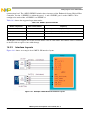
17.1 Supported Display Interfaces......................................................................................... 17-2
17.2 Adding Support for an LCD Panel................................................................................. 17-3
17.3 Modifying Boot Kernel Parameters to Support a New LCD ......................................... 17-5
17.3.1 Setting the Video Kernel Parameter........................................................................... 17-5
17.3.2 Setting the di1_primary Kernel Parameter ................................................................ 17-7
17.3.3 Modifying the Bits per Pixel Setting ......................................................................... 17-8
17.3.4 Modifying Display Timing for CLAA057VA01CT Using Kernel Parameters ......... 17-8
17.4 Adding Support for a New LCD .................................................................................. 17-10
17.4.1 Adding a Display Entry in the ltib Catalog.............................................................. 17-10
17.4.2 Creating the LCD Panel File (initialization, reset, power settings, backlight) ........ 17-11
17.4.3 Adding the Compilation Flag for the New Display ................................................. 17-12
17.4.4 Configuring LCD Timings and the Display Interface ............................................. 17-13
17.4.5 Adding BSP Support for a New Boot Command to Select CLAA057VA01CT LCD ......
17-14
17.5 i.MX53 Display Interface Helpful Information ........................................................... 17-15
Chapter 18
Connecting an LVDS Panel to an i.MX53 Reference Board
18.1 Connecting an LVDS Panel to the i.MX53 EVK Board................................................ 18-1
18.2 Enabling an LVDS Channel........................................................................................... 18-1
18.2.1 Locating Menu Configuration Options...................................................................... 18-2
18.2.2 Programming Interface .............................................................................................. 18-2
18.3 LDB Ports ...................................................................................................................... 18-3
18.3.1 Input Parallel Display Ports ....................................................................................... 18-4
18.3.2 Output LVDS Ports .................................................................................................... 18-4
18.4 Further Reading ............................................................................................................. 18-4
Chapter 19
Supporting the i.MX53 Camera Sensor Interface CSI0
19.1 Required Software ......................................................................................................... 19-1
19.2 i.MX53 CSI Interfaces Layout....................................................................................... 19-2
19.3 Configuring the CSI Unit in Test Mode......................................................................... 19-2
19.4 Adding Support for a New CMOS Camera Sensor ....................................................... 19-3
19.4.1 Adding a Camera Sensor Entry on the ltib Catalog (Kconfig) .................................. 19-3
19.4.2 Creating the Camera Sensor File ............................................................................... 19-4
19.4.3 Adding a Compilation Flag for the New Camera ...................................................... 19-5

i.MX53 System Development User’s Guide, Rev. 2
Freescale Semiconductor ix
Contents
Paragraph
Number Title
Page
Number
19.5 Using the I
2
C Interface .................................................................................................. 19-6
19.6 Loading and Testing the Camera Module...................................................................... 19-9
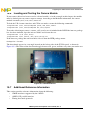
19.7 Additional Reference Information ................................................................................. 19-9
19.7.1 CMOS Interfaces Supported by the i.MX53............................................................ 19-10
19.7.2 i.MX53 CSI Parallel Interface ................................................................................. 19-11
19.7.3 Timing Data Mode Protocols................................................................................... 19-13
Chapter 20
Porting Audio Codecs to a Custom Board
20.1 Common Porting Task ................................................................................................... 20-1
20.2 Porting the Reference BSP to a Custom Board (audio codec is the same as in the reference
design)........................................................................................................................ 20-2
20.3 Porting the Reference BSP to a Custom Board (audio codec is different than the reference
design)........................................................................................................................ 20-2
Chapter 21
Porting the Fast Ethernet Controller Driver
21.1 Pin Configuration........................................................................................................... 21-1
21.2 Source Code................................................................................................................... 21-2
21.3 Ethernet Configuration................................................................................................... 21-2
Chapter 22
Porting USB Host1 and USB OTG
Appendix A
Revision History

i.MX53 System Development User’s Guide, Rev. 2
Freescale Semiconductor xi
Figures
Figure
Number Title
Page
Number
Figures
1-1 Boot Configuration Bus Isolation Resistors............................................................................ 1-8
2-1 i.MX53 Ball-Grid Array ......................................................................................................... 2-1
2-2 i.MX53 Package Information.................................................................................................. 2-2
2-3 i.MX53 Fanouts....................................................................................................................... 2-3
2-4 Layer Stack ............................................................................................................................. 2-4
2-5 Stackup Requirements............................................................................................................. 2-4
2-6 Connection Between i.MX53 and DDR2 and DDR3 ............................................................. 2-5
2-7 Final Placement of Memories and Decoupling Capacitors..................................................... 2-6
2-8 Topology for ADDR/CMD/CTRL Signals ............................................................................. 2-9
2-9 Topology of Data Group, Point-to-Point Connection ........................................................... 2-10
2-10 Topology for Data Bus of Two Byte Groups by Memory..................................................... 2-10
2-11 Clock Routing Topology ....................................................................................................... 2-11
2-12 ADDR/CMD Signal Routing ................................................................................................ 2-11
2-13 CTRL Signal Topology ......................................................................................................... 2-12
2-14 Data Bus Routing Topology.................................................................................................. 2-12
2-15 Clock Routing Topology ....................................................................................................... 2-12
2-16 Top DDR2 Routing .............................................................................................................. 2-13
2-17 Internal 1 DDR2 Routing...................................................................................................... 2-14
2-18 Power Plane 1 DDR2 Routing ............................................................................................. 2-15
2-19 Power Plane 2 DDR2 Routing ............................................................................................. 2-16
2-20 Internal 2 DDR2 Routing ..................................................................................................... 2-17
2-21 Bottom DDR2 Routing ........................................................................................................2-18
2-22 Top 8-DDR3 Routing ........................................................................................................... 2-21
2-23 Internal 1 8-DDR3 Routing ..................................................................................................2-22
2-24 Power Plane 1 8-DDR3 Routing .......................................................................................... 2-23
2-25 Power Plane 2 8-DDR3 Routing ........................................................................................... 2-24
2-26 Internal 2 8-DDR3 Routing ..................................................................................................2-25
2-27 Bottom 8-DDR3 Routing ..................................................................................................... 2-26
2-28 Microstrip and Stripline Differential Pair Dimensions ......................................................... 2-29
2-29 Differential Pair Routing....................................................................................................... 2-29
3-1 Model IV Keywords’ Structure............................................................................................... 3-4
3-2 Model Data Interpretation....................................................................................................... 3-6
3-3 Generic Test Load Network ....................................................................................................3-7
4-1 Internal LDOs ......................................................................................................................... 4-2
4-2 Power-up Sequence................................................................................................................. 4-3
4-3 Power Connections.................................................................................................................. 4-6
4-4 Communication Signal Connections....................................................................................... 4-7
4-5 Interface Power-up Sequence (DA9053)................................................................................. 4-8
4-6 Power-up Sequence................................................................................................................. 4-9
4-7 Power Connections Block (LT3481)..................................................................................... 4-12
4-8 Power Connections Block, cont. (LTC3589-1)..................................................................... 4-13

i.MX53 System Development User’s Guide, Rev. 2
xii Freescale Semiconductor
Figures
Figure
Number Title
Page
Number
4-9 Communication Signals Connections Block (LTC3589-1) .................................................. 4-14
4-10 Communication Signals Connections Block, cont. (TPS73201, LT3481)............................ 4-15
4-11 Interface Power-Up Sequence (LTC3589-1)......................................................................... 4-16
4-12 DA9053 Typical Application Block Diagram....................................................................... 4-18
4-13 LTC3589-1 Typical Application Block Guide ...................................................................... 4-21
5-1 Connection Between i.MX53 Processor and DDR2 and DDR3............................................. 5-2
5-2 DDR2 Memory Connection .................................................................................................... 5-3
5-3 DDR3 Memory Connection .................................................................................................... 5-4
5-4 Main Control Register........................................................................................................... 5-10
5-5 Power Down Register............................................................................................................ 5-11
5-6 Timing Configuration 0 Register .......................................................................................... 5-11
5-7 Timing Configuration 1 Register .......................................................................................... 5-12
8 ESDCTL Timing Configuration Register 2(ESDCFG2) ...................................................... 5-13
8-1 Example of Adding a Device .................................................................................................. 8-2
8-2 Updating the CoreSight Base Address.................................................................................... 8-3
8-3 i.MX/Cortex-A8 RVDS JTAG Scan Chain ............................................................................. 8-4
11-1 Linux Kernel Configuration Menu........................................................................................ 11-2
11-2 Android Memory Map (512 Mbyte System) ........................................................................ 11-4
11-3 Linux Kernel ......................................................................................................................... 11-5
11-4 Hardware Abstraction Layer................................................................................................. 11-6
14-1 Example i.MX53 Board SD Interface Layout....................................................................... 14-7
14-2 Second Example i.MX53 SD Interface Layout..................................................................... 14-8
15-1 Components of a Flash-Based File System........................................................................... 15-5
17-1 Available Display Interfaces ................................................................................................. 17-2
17-2 Interface................................................................................................................................. 17-4
17-3 Graphics Support Options Menu......................................................................................... 17-10
17-4 i.MX53 Board Display Interface Layout ............................................................................ 17-15
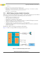
18-1 i.MX53 LVDS Display Bridge (LDB) Block........................................................................ 18-3
19-1 Camera Interface Layout....................................................................................................... 19-2
19-2 MXC Camera/V4L2 PRP Features Support Window........................................................... 19-3
19-3 Chessboard Test .................................................................................................................... 19-9
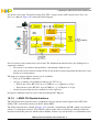
19-4 IPU Block Diagram............................................................................................................. 19-11
19-5 Parallel Interface Layout ..................................................................................................... 19-12

i.MX53 System Development User’s Guide, Rev. 2
Freescale Semiconductor xiii
Tables
Table
Number Title
Page
Number
Tab le s
i Conditional Tags and Settings Peculiar to this Chapter ............................................................xv
1-1 Design Checklist ..................................................................................................................... 1-1
1-2 DDR Vref Resistor Sizing Guideline...................................................................................... 1-8
1-3 I
2
C Bus Example Spreadsheet ................................................................................................ 1-9
1-4 I
2
C Port Usage Scenario ......................................................................................................... 1-9
1-5 JTAG Interface Summary...................................................................................................... 1-10
1-6 Additional JTAG Signals....................................................................................................... 1-10
2-1 DDR2/DDR3 Routing by the Same Length............................................................................ 2-7
2-2 DDR2/DDR3 Routing by Byte Group .................................................................................... 2-8
2-3 Total Signal Etch (DDR2) .................................................................................................... 2-19
2-4 Total Signal Etch (DDR3).....................................................................................................2-27
3-1 Header Information ................................................................................................................. 3-2
3-2 Component and Pin Information............................................................................................. 3-2
3-3 Ramp and Waveform Keywords ............................................................................................. 3-5
3-4 Golden Waveform Keywords .................................................................................................. 3-7
3-5 Unmodeled Analog or Special Interface Pins ....................................................................... 3-10
3-6 Unmodeled Differential Signals............................................................................................ 3-10
4-1 i.MX53 Voltage Rails and Associated DA9053 Regulator ..................................................... 4-4
4-2 i.MX53 Voltage Rails and Associated LTC3589-1 Regulator .............................................. 4-10
4-3 Generated Supply Domains .................................................................................................. 4-19
4-4 LTC3589-1 Supply Domains ................................................................................................ 4-21
6-1 Sample Voltage Report............................................................................................................ 6-1
6-2 Board Bring-Up Checklist ...................................................................................................... 6-3
7-1 Clock Roots............................................................................................................................. 7-1
11-1 Android Enhancements ......................................................................................................... 11-5
12-1 Configuration Files................................................................................................................ 12-2
12-2 IOMUX Configuration Files ................................................................................................. 12-4
13-1 Available Files—First Set ..................................................................................................... 13-2
13-2 Available Files—Second Set................................................................................................. 13-3
13-3 Available Files—Third Set.................................................................................................... 13-3
14-1 Structure Descriptions........................................................................................................... 14-2
14-2 ESDHC Pins.......................................................................................................................... 14-6
14-3 ESDHC Operation Modes..................................................................................................... 14-7
15-1 Parameter Variables............................................................................................................... 15-1
15-2 Device Information ............................................................................................................... 15-2
15-3 CSPI Parameters.................................................................................................................... 15-3
16-1 Files for Adding/Configuring a New Keypad ....................................................................... 16-1
17-1 Available Interfaces............................................................................................................... 17-2
17-2 Timing Parameters ................................................................................................................ 17-4
17-3 Parameter Information .......................................................................................................... 17-5
17-4 XGA DVI Monitor Example Variables................................................................................. 17-6

i.MX53 System Development User’s Guide, Rev. 2
xiv Freescale Semiconductor
Tables
Table
Number Title
Page
Number
17-5 VGA LCD Example Variables .............................................................................................. 17-7
17-6 720P TV Example Variables ................................................................................................. 17-7
17-7 Sample Values ....................................................................................................................... 17-9
17-8 Required Functions ............................................................................................................. 17-11
19-1 Settings for Test Mode .......................................................................................................... 19-2
19-2 Required Functions ............................................................................................................... 19-4
19-3 CSI0 Parallel Interface Signals ........................................................................................... 19-12
20-1 Required Power Supplies ...................................................................................................... 20-2
20-2 Files for sgtl Codec Support.................................................................................................. 20-2
21-1 RMII Signals ......................................................................................................................... 21-1
21-2 Source Code Files ................................................................................................................. 21-2
A-1 i.MX53 System Development User Guide Document Revision History.............................. 22-3

i.MX53 System Development User’s Guide, Rev. 2
Freescale Semiconductor xv
About This Guide
The i.MX53 multimedia applications processor (i.MX53) is Freescale Semiconductor, Inc.’s latest addition
to a growing family of multimedia-focused products that offer high performance processing optimized for
the lowest power consumption. The i.MX53 processors feature Freescale’s advanced implementation of
the ARM Cortex-A8™ core which operates at speeds as high as 1.2 GHz. The integrated memory
controller is compatible with DDR2-800, LVDDR2-800, and DDR3-800 DRAM, as well as LPDDR2-800
in the PoP package.
This product is suitable for applications such as:
• Automotive navigation and entertainment
• High-end mobile Internet devices and high-end PDAs
•Tablets
• Smart mobile devices
• High-end portable media players with HD video capability
• Portable navigation devices
• Gaming consoles
• Industrial HMI
Freescale provides a number of tools that facilitate the rapid design-in of the i.MX53 Applications
Processor for consumer, automotive, or industrial products. These tools include the i.MX53 software
developer’s kit (SDK), the i.MX53 Quick Start Board, the SABRE platform for tablets based on the
i.MX53, and the SABRE platform for automotive infotainment. These tools allow the rapid prototyping of
new products prior to commitment to production-level designs. Once you have determined the precise
features, function and physical parameters of your product, these prototyping tools along with this
document, the i.MX53 System Development User’s Guide, aid you in the design, layout, and bring-up of
your design.
Along with tips on designing your custom circuit board, this guide helps you customize Freescale provided
software utilizing the development tools provided in the SDK. This guide assumes that you have access to
generally available software tools (such as compilers, linkers and Make builders) as well as Freescale’s
Linux Target Image Builder (LTIB).
Table i. Conditional Tags and Settings Peculiar to this Chapter
Condition Tag
Name
Definition (Intended
Usage/Target Audience)
Draco
Settings
Dracom
Settings
Which Conditional Tags are
Showing or HIdden
ThisTagName is not hidden: where the
word ‘not’ is big, bold, and
conditionalized with the tag name in
column 1.

About This Guide
i.MX53 System Development User’s Guide, Rev. 2
xvi Freescale Semiconductor
Audience
This document is targeted to software and hardware engineers who desire to port the i.MX53 board support
package (BSP) to customer-specific products. The audience is expected to have a working understanding
of the ARM processor programming model, the C programming language, tools such as compilers and
assemblers, and program build tools such as MAKE. Familiarity with the use of commonly available
hardware test and debug tools such as oscilloscopes and logic analyzers is assumed. An understanding of
the architecture of the i.MX53 application processor is also assumed.
Organization
This guide is a compendium of application notes organized in two parts. The first part covers aspects of
hardware design and bring-up, and the second focuses on software development.
Part I, “Hardware Design and Bring-up” covers topics that aid you in the design of a custom printed circuit
board design utilizing the i.MX53. The following lists the chapters of Part I and provides a quick link to
each:
• Chapter 1, “Design Checklist”—provides a design checklist that contains recommendations for
optimal design for i.MX53-based systems.
• Chapter 2, “i.MX53 Layout Recommendations”—provides recommendations to assist design
engineers with the correct layout of their i.MX53x-based system.
• Chapter 3, “Understanding the IBIS Model”—explains how to use the IBIS (input output buffer
information specification) model.
• Chapter 4, “Setting up Power Management”—discusses how to supply and interface the i.MX53
multimedia applications processor with two different power management integrated circuits
(PMICs): DA9053 and LTC3589.
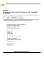
• Chapter 5, “Interfacing DDR2 and DDR3 Memories with the i.MX53 Processor”—explains the
interface between the i.MX53 processor and DDR2 and DDR3 memories. It includes the routing
guidelines, pictures, and examples.
• Chapter 6, “Avoiding Board Bring-Up Problems”—provides recommendations for avoiding
typical mistakes when bringing up a board for the first time.
• Chapter 7, “Using the Clock Connectivity Table”—explains how to use the i.MX53 clocking
connectivity.
• Chapter 8, “Configuring JTAG Tools for Debugging”—explains how to configure JTAG tools for
debugging.”
Part II, “Software Development” aids you in software development for your product. The first four
chapters are organized in the way a developer might approach the task of porting Freescale's SDK BSP to
support their target product board. The remaining chapters deal with porting selected integrated I/O
devices. The following lists the chapters of Part II and provides a quick link to each:
• Miriam, just continue the chapter numbering from Part I. Chapter 9, “Porting the
On-Board-Diagnostic-Suite (OBDS) to a Custom Board
• Chapter 10, “Porting U-Boot from an i.MX53 Reference Board to an i.MX53 Custom Board”
• Chapter 11, “Porting the Android Kernel”

About This Guide
i.MX53 System Development User’s Guide, Rev. 2
Freescale Semiconductor xvii
• Chapter 12, “Configuring the IOMUX Controller (IOMUXC)”
• Chapter 13, “Registering a New UART Driver”
• Chapter 5, “Interfacing DDR2 and DDR3 Memories with the i.MX53 Processor”
• Chapter 14, “Adding Support for the i.MX53 ESDHC”
• Chapter 15, “Configuring the SPI NOR Flash Memory Technology Device (MTD) Driver”
• Chapter 16, “Setting Up the Keypad Port (KPP)”
• Chapter 17, “Supporting the i.MX53 Reference Board DISP0 LCD”
• Chapter 18, “ Connecting an LVDS Panel to an i.MX53 Reference Board”
• Chapter 19, “ Supporting the i.MX53 Camera Sensor Interface CSI0”
• Chapter 20, “Porting Audio Codecs to a Custom Board”
• Chapter 21, “Porting the Fast Ethernet Controller Driver”
• Chapter 22, “Porting USB Host1 and USB OTG”
Essential Reference
You should have access to an electronic copy of the latest version of the i.MX53 Multimedia Applications
Processor Reference Manual (MCIMX53RM) and i.MX53xD Applications Processors for Consumer
Products (IMX53CEC).
Suggested Reading
This section lists additional reading that provides background for the information in this manual as well as
general information about the architecture.
General Information
The following documentation provides useful information about the ARM processor architecture and
computer architecture in general:
• For information about the ARM Cortex-A8 processor see
http://www.arm.com/products/processors/cortex-a/cortex-a8.php
• Computer Architecture: A Quantitative Approach, Fourth Edition, by John L. Hennessy and
David A. Patterson
• Computer Organization and Design: The Hardware/Software Interface, Second Edition, by
David A. Patterson and John L. Hennessy
Related Documentation
Freescale documentation is available from the sources listed on the back cover of this manual; the
document order numbers are included in parentheses for ease in ordering:
Additional literature is published as new Freescale products become available. For a current list of
documentation, refer to www.freescale.com.

About This Guide
i.MX53 System Development User’s Guide, Rev. 2
xviii Freescale Semiconductor
Conventions
This document uses the following notational conventions:
Courier Used to indicate commands, command parameters, code examples, and file and
directory names.
Italics Italics indicates command or function parameters
Bold Function names are written in bold.
cleared/set When a bit takes the value zero, it is said to be cleared; when it takes a value of
one, it is said to be set.
mnemonics Instruction mnemonics are shown in lowercase bold
Book titles in text are set in italics
sig_name Internal signals are written in all lowercase
0x0 Prefix to denote hexadecimal number
0b0 Prefix to denote binary number
rA, rB Instruction syntax used to identify a source GPR
rD Instruction syntax used to identify a destination GPR
REG[FIELD] Abbreviations for registers are shown in uppercase text. Specific bits, fields, or
ranges appear in brackets. For example, MSR[LE] refers to the little-endian mode
enable bit in the machine state register.
x In some contexts, such as signal encodings, an unitalicized x indicates a don’t
care.
x An italicized x indicates an alphanumeric variable
n, m An italicized n indicates a numeric variable
NOTE
In this guide, notation for all logical, bit-wise, arithmetic, comparison, and
assignment operations follow C Language conventions.
Signal Conventions
PWR_ON_RESET An overbar indicates that a signal is active when low
_b, _B Alternate notation indicating an active-low signal
signal_name Lowercase italics is used to indicate internal signals

About This Guide
i.MX53 System Development User’s Guide, Rev. 2
Freescale Semiconductor xix
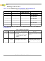
Acronyms and Abbreviations
The following table defines the acronyms and abbreviations used in this document.
Definitions and Acronyms
Term Definition
Address
Translation
Address conversion from virtual domain to physical domain
API Application Programming Interface
ARM
®
Advanced RISC Machines processor architecture
AUDMUX Digital audio multiplexer—provides a programmable interconnection for voice, audio, and synchronous data
routing between host serial interfaces and peripheral serial interfaces.
BCD Binary Coded Decimal
Bus A path between several devices through data lines.
Bus load The percentage of time a bus is busy.
CODEC Coder/decoder or compression/decompression algorithm—Used to encode and decode (or compress and
decompress) various types of data.
CPU Central Processing Unit—generic term used to describe a processing core.
CRC Cyclic Redundancy Check—Bit error protection method for data communication.
CSI Camera Sensor Interface
DMA Direct Memory Access—an independent block that can initiate memory-to-memory data transfers.
DRAM Dynamic Random Access Memory
EMI External Memory Interface—controls all IC external memory accesses (read/write/erase/program) from all
the masters in the system.
Endian Refers to byte ordering of data in memory. Little Endian means that the least significant byte of the data is
stored in a lower address than the most significant byte. In Big Endian, the order of the bytes is reversed.
EPIT Enhanced Periodic Interrupt Timer—a 32-bit set and forget timer capable of providing precise interrupts at
regular intervals with minimal processor intervention.
FCS Frame Checker Sequence
FIFO First In First Out
FIPS Federal Information Processing Standards—United States Government technical standards published by
the National Institute of Standards and Technology (NIST). NIST develops FIPS when there are compelling
Federal government requirements such as for security and interoperability but no acceptable industry
standards or solutions.
FIPS-140 Security requirements for cryptographic modules—Federal Information Processing Standard 140-2(FIPS
140-2) is a standard that describes US Federal government requirements that IT products should meet for
Sensitive, But Unclassified (SBU) use.
Flash A non-volatile storage device similar to EEPROM, but where erasing can only be done in blocks of the entire
chip.
Flash path Path within ROM bootstrap pointing to an executable Flash application.

About This Guide
i.MX53 System Development User’s Guide, Rev. 2
xx Freescale Semiconductor
Flush A procedure to reach cache coherency. Refers to removing a data line from cache. This process includes
cleaning the line, invalidating its VBR and resetting the tag valid indicator. The flush is triggered by a software
command.
GPIO General Purpose Input/Output
Hash Hash values are produced to access secure data. A hash value (or simply hash), also called a message
digest, is a number generated from a string of text. The hash is substantially smaller than the text itself, and
is generated by a formula in such a way that it is extremely unlikely that some other text will produce the
same hash value.
I/O Input/Output
ICE In-Circuit Emulation
IP Intellectual Property.
IPU Image Processing Unit —supports video and graphics processing functions and provides an interface to
video/still image sensors and displays.
IrDA Infrared Data Association—a nonprofit organization whose goal is to develop globally adopted specifications
for infrared wireless communication.
ISR Interrupt Service Routine.
JTAG JTAG (IEEE Standard 1149.1) A standard specifying how to control and monitor the pins of compliant
devices on a printed circuit board.
Kill Abort a memory access.
KPP KeyPad Port—a 16-bit peripheral that can be used as a keypad matrix interface or as general purpose
input/output (I/O).
line Refers to a unit of information in the cache that is associated with a tag.
LRU Least Recently Used—a policy for line replacement in the cache.
MMU Memory Management Unit—a component responsible for memory protection and address translation.
MPEG Moving Picture Experts Group—an ISO committee that generates standards for digital video compression
and audio. It is also the name of the algorithms used to compress moving pictures and video.
MPEG standards There are several standards of compression for moving pictures and video.
MPEG-1 is optimized for CD-ROM and is the basis for MP3.
MPEG-2 is defined for broadcast quality video in applications such as digital television set-top boxes and
DVD.
MPEG-3 was merged into MPEG-2.
MPEG-4 is a standard for low-bandwidth video telephony and multimedia on the World-Wide Web.
MQSPI Multiple Queue Serial Peripheral Interface—used to perform serial programming operations necessary to
configure radio subsystems and selected peripherals.
MSHC Memory Stick Host Controller
NAND Flash Flash ROM technology—NAND Flash architecture is one of two flash technologies (the other being NOR)
used in memory cards such as the Compact Flash cards. NAND is best suited to flash devices requiring high
capacity data storage. NAND flash devices offer storage space up to 512-Mbyte and offer faster erase, write,
and read capabilities over NOR architecture.
NOR Flash See NAND Flash.
Definitions and Acronyms (continued)
Term Definition

About This Guide
i.MX53 System Development User’s Guide, Rev. 2
Freescale Semiconductor xxi
PCMCIA Personal Computer Memory Card International Association—a multi-company organization that has
developed a standard for small, credit card-sized devices, called PC Cards. There are three types of
PCMCIA cards that have the same rectangular size (85.6 by 54 millimeters), but different widths.
Physical address The address by which the memory in the system is physically accessed.
PLL Phase Locked Loop—an electronic circuit controlling an oscillator so that it maintains a constant phase
angle (a lock) on the frequency of an input, or reference, signal.
RAM Random Access Memory
RAM path Path within ROM bootstrap leading to the downloading and the execution of a RAM application
RGB The RGB color model is based on the additive model in which Red, Green, and Blue light are combined in
various ways to create other colors. The abbreviation RGB come from the three primary colors in additive
light models.
RGBA RGBA color space stands for Red Green Blue Alpha. The alpha channel is the transparency channel, and
is unique to this color space. RGBA, like RGB, is an additive color space, so the more of a color you place,
the lighter the picture gets. PNG is the best known image format that uses the RGBA color space.
RNGA Random Number Generator Accelerator—a security hardware module that produces 32-bit pseudo random
numbers as part of the security module.
ROM Read Only Memory
ROM bootstrap Internal boot code encompassing the main boot flow as well as exception vectors.
RTIC Real-time integrity checker—a security hardware module
SCC SeCurity Controller—a security hardware module
SDMA Smart Direct Memory Access
SDRAM Synchronous Dynamic Random Access Memory
SoC System on a Chip
SPBA Shared Peripheral Bus Arbiter—a three-to-one IP-Bus arbiter, with a resource-locking mechanism.
SPI Serial Peripheral Interface—a full-duplex synchronous serial interface for connecting
low-/medium-bandwidth external devices using four wires. SPI devices communicate using a master/slave
relationship over two data lines and two control lines: Also see SS, SCLK, MISO, and MOSI.
SRAM Static Random Access Memory
SSI Synchronous-Serial Interface—standardized interface for serial data transfer
TBD To Be Determined
UART Universal Asynchronous Receiver/Transmitter—this module provides asynchronous serial communication
to external devices.
UID Unique ID–a field in the processor and CSF identifying a device or group of devices
USB Universal Serial Bus—an external bus standard that supports high speed data transfers. The USB 1.1
specification supports data transfer rates of up to 12Mb/s and USB 2.0 has a maximum transfer rate of
480 Mbps. A single USB port can be used to connect up to 127 peripheral devices, such as mice, modems,
and keyboards. USB also supports Plug-and-Play installation and hot plugging.
Definitions and Acronyms (continued)
Term Definition

About This Guide
i.MX53 System Development User’s Guide, Rev. 2
xxii Freescale Semiconductor
USBOTG USB On The Go—an extension of the USB 2.0 specification for connecting peripheral devices to each other.
USBOTG devices, also known as dual-role peripherals, can act as limited hosts or peripherals themselves
depending on how the cables are connected to the devices, and they also can connect to a host PC.
Word A group of bits comprising 32 bits
Definitions and Acronyms (continued)
Term Definition
Page is loading ...
Page is loading ...
Page is loading ...
Page is loading ...
Page is loading ...
Page is loading ...
Page is loading ...
Page is loading ...
Page is loading ...
Page is loading ...
Page is loading ...
Page is loading ...
Page is loading ...
Page is loading ...
Page is loading ...
Page is loading ...
Page is loading ...
Page is loading ...
Page is loading ...
Page is loading ...
Page is loading ...
Page is loading ...
Page is loading ...
Page is loading ...
Page is loading ...
Page is loading ...
Page is loading ...
Page is loading ...
Page is loading ...
Page is loading ...
Page is loading ...
Page is loading ...
Page is loading ...
Page is loading ...
Page is loading ...
Page is loading ...
Page is loading ...
Page is loading ...
Page is loading ...
Page is loading ...
Page is loading ...
Page is loading ...
Page is loading ...
Page is loading ...
Page is loading ...
Page is loading ...
Page is loading ...
Page is loading ...
Page is loading ...
Page is loading ...
Page is loading ...
Page is loading ...
Page is loading ...
Page is loading ...
Page is loading ...
Page is loading ...
Page is loading ...
Page is loading ...
Page is loading ...
Page is loading ...
Page is loading ...
Page is loading ...
Page is loading ...
Page is loading ...
Page is loading ...
Page is loading ...
Page is loading ...
Page is loading ...
Page is loading ...
Page is loading ...
Page is loading ...
Page is loading ...
Page is loading ...
Page is loading ...
Page is loading ...
Page is loading ...
Page is loading ...
Page is loading ...
Page is loading ...
Page is loading ...
Page is loading ...
Page is loading ...
Page is loading ...
Page is loading ...
Page is loading ...
Page is loading ...
Page is loading ...
Page is loading ...
Page is loading ...
Page is loading ...
Page is loading ...
Page is loading ...
Page is loading ...
Page is loading ...
Page is loading ...
Page is loading ...
Page is loading ...
Page is loading ...
Page is loading ...
Page is loading ...
Page is loading ...
Page is loading ...
Page is loading ...
Page is loading ...
Page is loading ...
Page is loading ...
Page is loading ...
Page is loading ...
Page is loading ...
Page is loading ...
Page is loading ...
Page is loading ...
Page is loading ...
Page is loading ...
Page is loading ...
Page is loading ...
Page is loading ...
Page is loading ...
Page is loading ...
Page is loading ...
Page is loading ...
Page is loading ...
Page is loading ...
Page is loading ...
Page is loading ...
Page is loading ...
Page is loading ...
Page is loading ...
Page is loading ...
Page is loading ...
Page is loading ...
Page is loading ...
Page is loading ...
Page is loading ...
Page is loading ...
Page is loading ...
Page is loading ...
Page is loading ...
Page is loading ...
Page is loading ...
Page is loading ...
Page is loading ...
Page is loading ...
Page is loading ...
Page is loading ...
Page is loading ...
Page is loading ...
Page is loading ...
Page is loading ...
Page is loading ...
Page is loading ...
Page is loading ...
Page is loading ...
Page is loading ...
Page is loading ...
Page is loading ...
Page is loading ...
Page is loading ...
Page is loading ...
Page is loading ...
Page is loading ...
Page is loading ...
Page is loading ...
Page is loading ...
Page is loading ...
Page is loading ...
Page is loading ...
Page is loading ...
Page is loading ...
Page is loading ...
Page is loading ...
Page is loading ...
Page is loading ...
Page is loading ...
Page is loading ...
Page is loading ...
Page is loading ...
Page is loading ...
Page is loading ...
Page is loading ...
Page is loading ...
Page is loading ...
Page is loading ...
Page is loading ...
Page is loading ...
Page is loading ...
Page is loading ...
Page is loading ...
Page is loading ...
Page is loading ...
Page is loading ...
Page is loading ...
-
 1
1
-
 2
2
-
 3
3
-
 4
4
-
 5
5
-
 6
6
-
 7
7
-
 8
8
-
 9
9
-
 10
10
-
 11
11
-
 12
12
-
 13
13
-
 14
14
-
 15
15
-
 16
16
-
 17
17
-
 18
18
-
 19
19
-
 20
20
-
 21
21
-
 22
22
-
 23
23
-
 24
24
-
 25
25
-
 26
26
-
 27
27
-
 28
28
-
 29
29
-
 30
30
-
 31
31
-
 32
32
-
 33
33
-
 34
34
-
 35
35
-
 36
36
-
 37
37
-
 38
38
-
 39
39
-
 40
40
-
 41
41
-
 42
42
-
 43
43
-
 44
44
-
 45
45
-
 46
46
-
 47
47
-
 48
48
-
 49
49
-
 50
50
-
 51
51
-
 52
52
-
 53
53
-
 54
54
-
 55
55
-
 56
56
-
 57
57
-
 58
58
-
 59
59
-
 60
60
-
 61
61
-
 62
62
-
 63
63
-
 64
64
-
 65
65
-
 66
66
-
 67
67
-
 68
68
-
 69
69
-
 70
70
-
 71
71
-
 72
72
-
 73
73
-
 74
74
-
 75
75
-
 76
76
-
 77
77
-
 78
78
-
 79
79
-
 80
80
-
 81
81
-
 82
82
-
 83
83
-
 84
84
-
 85
85
-
 86
86
-
 87
87
-
 88
88
-
 89
89
-
 90
90
-
 91
91
-
 92
92
-
 93
93
-
 94
94
-
 95
95
-
 96
96
-
 97
97
-
 98
98
-
 99
99
-
 100
100
-
 101
101
-
 102
102
-
 103
103
-
 104
104
-
 105
105
-
 106
106
-
 107
107
-
 108
108
-
 109
109
-
 110
110
-
 111
111
-
 112
112
-
 113
113
-
 114
114
-
 115
115
-
 116
116
-
 117
117
-
 118
118
-
 119
119
-
 120
120
-
 121
121
-
 122
122
-
 123
123
-
 124
124
-
 125
125
-
 126
126
-
 127
127
-
 128
128
-
 129
129
-
 130
130
-
 131
131
-
 132
132
-
 133
133
-
 134
134
-
 135
135
-
 136
136
-
 137
137
-
 138
138
-
 139
139
-
 140
140
-
 141
141
-
 142
142
-
 143
143
-
 144
144
-
 145
145
-
 146
146
-
 147
147
-
 148
148
-
 149
149
-
 150
150
-
 151
151
-
 152
152
-
 153
153
-
 154
154
-
 155
155
-
 156
156
-
 157
157
-
 158
158
-
 159
159
-
 160
160
-
 161
161
-
 162
162
-
 163
163
-
 164
164
-
 165
165
-
 166
166
-
 167
167
-
 168
168
-
 169
169
-
 170
170
-
 171
171
-
 172
172
-
 173
173
-
 174
174
-
 175
175
-
 176
176
-
 177
177
-
 178
178
-
 179
179
-
 180
180
-
 181
181
-
 182
182
-
 183
183
-
 184
184
-
 185
185
-
 186
186
-
 187
187
-
 188
188
-
 189
189
-
 190
190
-
 191
191
-
 192
192
-
 193
193
-
 194
194
-
 195
195
-
 196
196
-
 197
197
-
 198
198
-
 199
199
-
 200
200
-
 201
201
-
 202
202
-
 203
203
-
 204
204
-
 205
205
-
 206
206
-
 207
207
-
 208
208
-
 209
209
-
 210
210
-
 211
211
-
 212
212


NXP i.MX537 User guide
- Category
- Software
- Type
- User guide
Ask a question and I''ll find the answer in the document
Finding information in a document is now easier with AI
Related papers
Other documents
-
Dahua SDZ4032-HNR-ZB User manual
-
Freescale Semiconductor MCIMX53SMD Hardware User's Manual
-
 Mandik Control system User guide
-
-
Diamond Systems Aries User manual
-
LXE MX5 User manual
-
-
Digi ConnectCore i.MX53 User manual
-
-
