Kingston Technology KVR667D2Q8F5/4GHE Datasheet
- Category
- Memory modules
- Type
- Datasheet
This manual is also suitable for
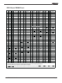
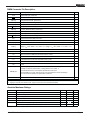
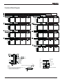
Kingston Technology KVR667D2Q8F5/4GHE is a 4GB, 512M x 72-bit PC2-5300 Fully buffered ECC SDRAM memory module designed for use in high-performance computing applications. This module is based on thirty-six 128M x 8-bit 667MHz DDR2 FBGA components and features a CAS latency of 5-5-5. It operates at a voltage of 1.8V and is RoHS compliant. This module is ideal for use in servers, workstations, and other high-performance computing applications where reliability and performance are critical.
Kingston Technology KVR667D2Q8F5/4GHE is a 4GB, 512M x 72-bit PC2-5300 Fully buffered ECC SDRAM memory module designed for use in high-performance computing applications. This module is based on thirty-six 128M x 8-bit 667MHz DDR2 FBGA components and features a CAS latency of 5-5-5. It operates at a voltage of 1.8V and is RoHS compliant. This module is ideal for use in servers, workstations, and other high-performance computing applications where reliability and performance are critical.


-
 1
1
-
 2
2
-
 3
3
-
 4
4
-
 5
5
-
 6
6
-
 7
7


Kingston Technology KVR667D2Q8F5/4GHE Datasheet
- Category
- Memory modules
- Type
- Datasheet
- This manual is also suitable for
Kingston Technology KVR667D2Q8F5/4GHE is a 4GB, 512M x 72-bit PC2-5300 Fully buffered ECC SDRAM memory module designed for use in high-performance computing applications. This module is based on thirty-six 128M x 8-bit 667MHz DDR2 FBGA components and features a CAS latency of 5-5-5. It operates at a voltage of 1.8V and is RoHS compliant. This module is ideal for use in servers, workstations, and other high-performance computing applications where reliability and performance are critical.
Ask a question and I''ll find the answer in the document
Finding information in a document is now easier with AI
Related papers
-
Kingston Technology KVR667D2D4F5/4GEF Datasheet
-
-
-
-
-
-
-
-
-
Other documents
-
Integral IN1T2GRSWCX2K2 Datasheet
-
Samsung M393T2950GZ3-CD5 Datasheet
-
Dataram DTM63392F Datasheet
-
-
Transcend TSCBU2 Datasheet
-
 SMART Modular SM646UDR26485-2-I Datasheet
-
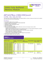 Aeneon AET961FB00-30D Datasheet
-
 Hynix HMP125U6EFR8C-S6 Datasheet
-
Silicon Power SP001GBLRU800S02 Datasheet
-


