Microsemi SmartFusion User guide

Type
User guide

Microsemi SmartFusion is a powerful system-on-chip (SoC) FPGA that combines an ARM Cortex-M3 processor with a high-performance FPGA fabric, offering a unique combination of processing power and programmable logic. This device is ideal for a wide range of applications, including industrial automation, motor control, medical imaging, and automotive systems. With its low power consumption, small form factor, and high reliability, SmartFusion is a great choice for space-constrained and power-sensitive applications.

Microsemi SmartFusion is a powerful system-on-chip (SoC) FPGA that combines an ARM Cortex-M3 processor with a high-performance FPGA fabric, offering a unique combination of processing power and programmable logic. This device is ideal for a wide range of applications, including industrial automation, motor control, medical imaging, and automotive systems. With its low power consumption, small form factor, and high reliability, SmartFusion is a great choice for space-constrained and power-sensitive applications.
SmartFusion
Dedicated Fabric Clock Conditioning Circuit with PLL
Integration
Libero® IDE Software
Revision 1 2
Table of Contents
1 Configuration Options. . . . . . . . . . . . . . . . . . . . . . . . . . . . . . . . . . . . . . . . . . . . . . . . . . . . . . . . . . . . . . . 3
CLK<x> (x= A/B/C) Input Clocks . . . . . . . . . . . . . . . . . . . . . . . . . . . . . . . . . . . . . . . . . . . . . . . . . . . . . . . . . . . . . . . 4
2 Port Description . . . . . . . . . . . . . . . . . . . . . . . . . . . . . . . . . . . . . . . . . . . . . . . . . . . . . . . . . . . . . . . . . . . 9
A Product Support . . . . . . . . . . . . . . . . . . . . . . . . . . . . . . . . . . . . . . . . . . . . . . . . . . . . . . . . . . . . . . . . . . 11
Contacting the Customer Technical Support Center . . . . . . . . . . . . . . . . . . . . . . . . . . . . . . . . . . . . . . . . . . . . . . . 11
Non-Technical Customer Service . . . . . . . . . . . . . . . . . . . . . . . . . . . . . . . . . . . . . . . . . . . . . . . . . . . . . . . . . . . . . 11
Revision 1 3
1 – Configuration Options
The Fabric Clock Conditioning Circuit (FAB_CCC) Configurator enables you to configure the second
CCC/PLL block available only in the A2F500 device. This CCC/PLL is dedicated to the FPGA fabric.
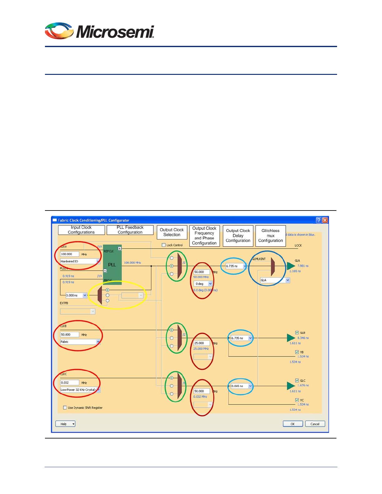
The Fabric CCC can condition up to three input clocks and generate up to three global clocks. The
configuration of the CCC can be broken down in the following four major blocks:
Input reference clocks (CLKx) configuration
Output Clocks (GLx) configuration
Clock source selection
Clock frequency and phase configurations
Clock delay configurations
PLL feedback clock selection
Glitch less clock multiplexing configuration
The Fabric Clock Conditioning Circuitry (FAB_CCC) is configured using flash cells based on the
selection made in this configurator. You can also override the static configuration by using the
configuration shift register available on the FAB_CCC block.
The Dedicated Fabric Clock Conditioning Circuit is shown in Figure 1-1.
Figure 1-1FAB_CCC Configuration Options
4 Revision 1
CLK<x> (x= A/B/C) Input Clocks
To configure the CLK<x> reference clock, first select the clock source, then define the clock source.
Clock Source Selection
The following sources are available from the reference clock pull-down menu:
External I/O - The clock source can be any fabric I/O. The regular FPGA I/O is routed to the
reference clock fabric interface pin.
Hardwired I/O - The clock source is one of three regular FPGA I/Os that has a dedicated path to
drive the reference clock.
Hardwired I/O (LVPECL) - The clock source is one of two regular FPGA I/Os (P side of the
LVPECL pair) that has a dedicated path to drive the reference clock.
Hardwired I/O (LVDS) - The clock source is one of two regular FPGA I/Os (P side of the LVDS
pair) that has a dedicated path to drive the reference clock.
Internal logic - The clock source can be any FPGA fabric logic.
On-chip RC Oscillator - The clock source is a dedicated 100 MHz On-chip RC Oscillator
available on the SmartFusion device. The on-chip RC oscillator is actually generated as part of
the MSS clock configurator. Refer to the MSS_CCC Configurator for details of how to export the
on-chip RC oscillator output port.
Main Crystal Oscillator - The source is an external Crystal or an external RC circuit connected
to the main crystal oscillator external pins. See the Actel SmartFusion Microcontroller Subsystem
User's Guide for details about how the external crystal must be connected on the board to the
SmartFusion device. This option is only available for CLKA and CLKB. The main crystal oscillator
is actually generated as part of the MSS clock configurator. Refer to the MSS_CCC Configurator
for details on how to export the main crystal oscillator output port.
Clock Frequency
You must specify the clock source frequency. Note the following frequency requirements:
The On-chip Oscillator clock frequency is fixed to 100 MHz and cannot be changed.
The Main Crystal Oscillator clock frequency must be between 1.5 MHz and 20 MHz when the PLL
is used or between 32 KHz and 20 MHz when the PLL is bypassed. Use the same frequency as
the one specified in the MSS_CCC configurator for the main crystal oscillator.
The Main Crystal Oscillator (RC network configuration) clock frequency must be between 1.5
MHz and 4 MHz when the PLL is used or between 32 KHz and 4 MHz when the PLL is bypassed.
Use the same frequency as the one specified in the MSS_CCC configurator for the main crystal
oscillator.
For all other sources, the source clock frequency must be between 1.5 MHz and 176 MHz when
the PLL is used or between 32 KHz and 350 MHz when the PLL is bypassed.
GLx Output Clocks
GLA is always enabled. You may optionally enable the GLB (YB) and GLC (YC) clocks. The GLA, GLB
and GLC clock drive a global network in the FPGA fabric; the YB and YC drive local routing resources in
the FPGA. If you enable only the YB or YC output, the GLB or GLC global network cannot be used any
more.
Clock Source Selection - The source of the GLx clocks can either be:
Derived from the corresponding input clock CLKx (bypass mode). It can be a division of the
input clock.
Derived from the CLKA reference clock using one of the PLL 4 output VCO phases.
Derived from the CLKA reference clock using the PLL output VCO (phase 0) with a
programmable delay.
Libero® IDE Software
Revision 1 5
Clock Frequency - You must specify the output clock frequencies. This frequency is used by the
FAB_CCC configuration engine to automatically compute the CCC dividers to meet your
frequency requirements. The dividers are highlighted in blue (for instance /2) in the configurator
UI.
Phase Configuration - The PLL block offers 4 phases that you can access through the phase
selection pull-down menu. The actual phases and resulting delays are highlighted in blue on the
configurator UI. The actual phase is not the same as the selected phase if the output divider is not
1 (actual_phase = selected_phase / output_divider). The actual delay is a function of the actual
phase of the PLL output (VCO).
Delay Configuration - For GLx only, you may configure the programmable delay to further tune
the overall CLKA to GLx delays (when the PLL is used) or CLKx to GLx delays (when the bypass
mode is used) based on your system requirements. The programmable delays are typical delays.
The total delays are highlighted in blue in the configurator UI. The delays provided by the
configurator are typical delays and match those computed by SmartTime typical conditions.
PLL Feedback Clock
PLL Feedback Source - If the you use the PLL, you can choose to use an internal or an external
feedback loop depending on your system level requirements:
Internal feedback from VCO (phase 0) without programmable delay - This is the default
choice.
Internal feedback from VCO (phase 0) with programmable delay - Use a fine grain
programmable delay to tune your overall CCC delays based on your system requirements.
The programmable delays are typical delays
External I/O - The clock source can be any regular FPGA I/O. The regular FPGA I/O is routed
to the feedback clock fabric interface pin.
Hardwired I/O - The clock source is one of three regular FPGA I/Os that has a dedicated path
to drive the feedback clock.
Hardwired I/O (LVPECL) - The clock source is one of two regular FPGA I/Os (P side of the
LVPECL pair) that has a dedicated path to drive the feedback clock.
Hardwired IO (LVDS) - The clock source is one of two regular FPGA I/Os (P side of the LVDS
pair) that has a dedicated path to drive the feedback clock.
Fabric - The clock source can be any FPGA fabric logic.
Programmable Fix Delay - You can also add a fix delay (~2 ns typical) to your feedback loop. This
delay has been defined to be about the same delay as the clock network within the FPGA (GLx to
the input of a flip-flop).
Note: When the PLL is used with an external feedback, all engine computations are based on the
assumptions that the external feedback is driven from the GLA fabric CCC output whether through
the fabric or externally to the chip. The engine also assumes a delay of 0 ns for the path from GLA
to the fabric CCC external feedback input. To have the correct delays at the system level you must
adjust the delay computation based on the actual typical external delay.
Glitchless Clock Multiplexing
You can configure the glitch less clock multiplexor as follows:
GLA - No dynamic multiplexing is available and the GLA output comes from the CCC internal
GLA signal.
GLA_GLC - You can make a glitchless switch between the CCC internal GLA signal and the CCC
internal GLC signal. The output of the glitchless clock multiplexor comes out on the GLA global
network.
GLA_GLMUXINT - You can make a glitchless switch between the CCC internal GLA signal and
the FPGA fabric signal GLMUXINT. The output of the glitchless clock multiplexor comes out on
the GLA global network.
6 Revision 1
Dynamic Shift Register
You can dynamically configure or re-configure the Fabric CCC in your design by using the CCC
configuration dynamic shift register. Click the Use Dynamic Shift Register check box to enable this
option. The ports used to configure this register are SDIN, SCLK, SSHIFT, SUPDATE, SDOUT and
MODE and are described in "Port Description" on page 9.
Table 1-1 describes the CCC configuration shift register from SDIN to SDOUT. This table can be
generated from the Designer Software Tools > Report > Global > CCC_Configuration menu after layout
is complete. You must complete layout because as some configuration bits can only be computed based
on the placement of the design. The columns are defined as follows:
NAME - The configuration signal as defined on the FAB_CCC_DYN CAE macro.
SDIN - The register bit numbers.
VALUE - The configuration value as defined in the configurator and assigned to the configuration
signal.
TYPE - The type of the configuration with respect to what you are allowed to change when using
the CCC configuration shift register. Configuration bits marked EDIT can be safely changed by
you. Those marked MASKED should not be changed as they are defined by the placement of the
design. Finally, configurations marked READONLY should not be changed.
Table 1-1 • CCC Configuration Shift Register from SDIN to SDOUT
NAME SDIN VALUE TYPE
FINDIV [6: 0] 0010010 EDIT
FBDIV [13: 7] 0010010 EDIT
OADIV [18:14] 00001 EDIT
OBDIV [23:19] 00000 EDIT
OCDIV [28:24] 00000 EDIT
OAMUX [31:29] 100 EDIT
OBMUX [34:32] 000 EDIT
OCMUX [37:35] 000 EDIT
FBSEL [39:38] 01 EDIT
FBDLY [44:40] 00000 EDIT
XDLYSEL [45] 1 EDIT
DLYGLA [50:46] 00011 EDIT
DLYGLB [55:51] 11111 EDIT
DLYGLC [60:56] 00000 EDIT
DLYA0 [65:61] 00000 EDIT
DLYA1 [70:66] 00000 EDIT
STATASEL [71] 0 MASKED
STATBSEL [72] 1 MASKED
STATCSEL [73] 1 MASKED
Libero® IDE Software
Revision 1 7
For more details about the architecture of the SmartFusion fabric CCC and the definition of the
configuration bits, please refer to the Actel SmartFusion FPGA Fabric User's Guide.
VCOSEL [76:74] 000 EDIT
RESETEN [80] 1 READONLY
RXASEL [81] 0 MASKED
RXBSEL [82] 0 MASKED
RXCSEL [83] 0 MASKED
OADIVHALF [84] 0 EDIT
OBDIVHALF [85] 0 EDIT
OCDIVHALF [86] 0 EDIT
GLMUXCFG [88:87] 00 MASKED
Table 1-1 • CCC Configuration Shift Register from SDIN to SDOUT
NAME SDIN VALUE TYPE
Revision 1 9
2 – Port Description
In Table 2-1, 'x' indicates A, B or C.
Table 2-1 • FAB_CCC Port Description
Port Name Direction PAD? Description
CLKx IN No Reference clock when driven from Internal Logic or External I/O
CLKx_PAD IN Yes Reference clock when driven from Hardwired I/O
CLKx_PADP IN Yes Reference clock P side when driven from Hardwired I/O (LVDS) or
Hardwired I/O (LVPECL)
CLKx_PADN IN Yes Reference clock N side when driven from Hardwired I/O (LVDS) or
Hardwired I/O (LVPECL)
RCOSC IN No Reference clock when driven from On-chip RC Oscillator
MAINXIN IN No Reference clock when driven from Main Crystal Oscillator
EXTFB IN No PLL feedback clock when driven from Internal Logic or External I/O
EXTFB_PAD IN Yes PLL feedback clock when driven from Hardwired I/O
EXTFB_PADP IN Yes PLL feedback clock P side when driven from Hardwired I/O (LVDS) or
Hardwired I/O (LVPECL)
EXTFB_PADN IN Yes PLL feedback clock N side when driven from Hardwired I/O (LVDS) or
Hardwired I/O (LVPECL)
GLx OUT No Generated clock driving clock FPGA fabric global network 'x'
Yx OUT No Generated clock driving clock FPGA fabric local routing resource
OxDIVRST IN No OxDIVRST is available when the GLx or Yx output is not derived from the
PLL VCO output; it is in bypass mode with an output divider greater than 1.
The purpose of the OADIVRST signal is to reset the output of the final clock
divider to synchronize it with the input to that divider when the PLL is
bypassed.
The signal is active on a low to high transition. The signal must be low for at
least one divider input.
PLLEN IN No PLL Enable signal; this signal is active high or low based on the polarity
chosen in the configurator.
LOCK OUT No PLL Lock indicator signal; this signal is asserted (lock) high or low based on
the polarity chosen in the configurator
GLMUXINT IN No FPGA fabric input to the CCC glitchless MUX
GLMUXSEL IN No FPGA fabric input used to make a glitchless switch between GLA and
GLMUXINT or GLA and GLC.
SDIN IN No Dynamic shift register serial data in
10 Revision 1
SCLK IN No Dynamic shift register serial clock
SSHIFT IN No Dynamic shift register serial shift data command; the data present on SDIN is
shifted into the CCC configuration shift register on the rising edge of SCLK.
SUPDATE IN No Dynamic shift register serial data update; the data present in the shift register
is applied to the CCC as a new configuration
SDOUT OUT No Dynamic shift register serial data out; the last bit of the CCC configuration
shift register
MODE IN No If MODE is 0, the CCC configuration data is coming from the CCC
configuration register else it is coming from the programmed flash cells
Table 2-1 • FAB_CCC Port Description
Port Name Direction PAD? Description
Revision 1 11
A – Product Support
The Microsemi SoC Products Group backs its products with various support services including a
Customer Technical Support Center and Non-Technical Customer Service. This appendix contains
information about contacting the SoC Products Group and using these support services.
Contacting the Customer Technical Support Center
Microsemi staffs its Customer Technical Support Center with highly skilled engineers who can help
answer your hardware, software, and design questions. The Customer Technical Support Center spends
a great deal of time creating application notes and answers to FAQs. So, before you contact us, please
visit our online resources. It is very likely we have already answered your questions.
Technical Support
Microsemi customers can receive technical support on Microsemi SoC products by calling Technical
Support Hotline anytime Monday through Friday. Customers also have the option to interactively submit
and track cases online at My Cases or submit questions through email anytime during the week.
Web: www.actel.com/mycases
Phone (North America): 1.800.262.1060
Phone (International): +1 650.318.4460
ITAR Technical Support
Microsemi customers can receive ITAR technical support on Microsemi SoC products by calling ITAR
Technical Support Hotline: Monday through Friday, from 9 AM to 6 PM Pacific Time. Customers also
have the option to interactively submit and track cases online at My Cases or submit questions through
email anytime during the week.
Web: www.actel.com/mycases
Phone (North America): 1.888.988.ITAR
Phone (International): +1 650.318.4900
Email: soc_tech_itar@microsemi.com
Non-Technical Customer Service
Contact Customer Service for non-technical product support, such as product pricing, product upgrades,
update information, order status, and authorization.
Microsemi’s customer service representatives are available Monday through Friday, from 8 AM to 5 PM
Pacific Time, to answer non-technical questions.
Phone: +1 650.318.2470
5-02-00274-0/06.10
SoC Products Group (Hong Kong)
Room 2107, China Resources Building
26 Harbour Road
Wanchai, Hong Kong
Phone +852 2185 6460
Fax +852 2185 6488
© 2010 Microsemi Corporation. All rights reserved. Microsemi and the Microsemi logo are trademarks of Microsemi Corporation. All other trademarks and service marks
are the property of their respective owners.
SoC Products Group
2061 Stierlin Court
Mountain View, CA
94043-4655
USA
Phone 650.318.4200
Fax 650.318.4600
www.actel.com
SoC Products Group (Europe)
River Court, Meadows Business Park
Station Approach, Blackwatery
Camberley Surrey GU17 9AB
United Kingdom
Phone +44 (0) 1276 609 300
Fax +44 (0) 1276 607 540
SoC Products Group (Japan)
EXOS Ebisu Building 4F
1-24-14 Ebisu Shibuya-ku
Tokyo 150 Japan
Phone +81.03.3445.7671
Fax +81.03.3445.7668
Microsemi Corporation (NASDAQ: MSCC) offers the industry’s most comprehensive portfolio of semiconductor technology.
Committed to solving the most critical system challenges, Microsemi’s products include high-performance, high-reliability analog
and RF devices, mixed signal integrated circuits, FPGAs and customizable SoCs, and complete subsystems. Microsemi serves
leading system manufacturers around the world in the defense, security, aerospace, enterprise, commercial, and industrial
markets. Learn more at www.microsemi.com.
Corporate Headquarters
Microsemi Corporation
2381 Morse Avenue
Irvine, CA
92614-6233
USA
Phone 949-221-7100
Fax 949-756-0308
  • Page 1 1
  • Page 2 2
  • Page 3 3
  • Page 4 4
  • Page 5 5
  • Page 6 6
  • Page 7 7
  • Page 8 8
  • Page 9 9
  • Page 10 10
  • Page 11 11
  • Page 12 12

Microsemi SmartFusion User guide

Type
User guide

Microsemi SmartFusion is a powerful system-on-chip (SoC) FPGA that combines an ARM Cortex-M3 processor with a high-performance FPGA fabric, offering a unique combination of processing power and programmable logic. This device is ideal for a wide range of applications, including industrial automation, motor control, medical imaging, and automotive systems. With its low power consumption, small form factor, and high reliability, SmartFusion is a great choice for space-constrained and power-sensitive applications.

Ask a question and I''ll find the answer in the document

Finding information in a document is now easier with AI