Libero® IDE Software
Revision 1 5
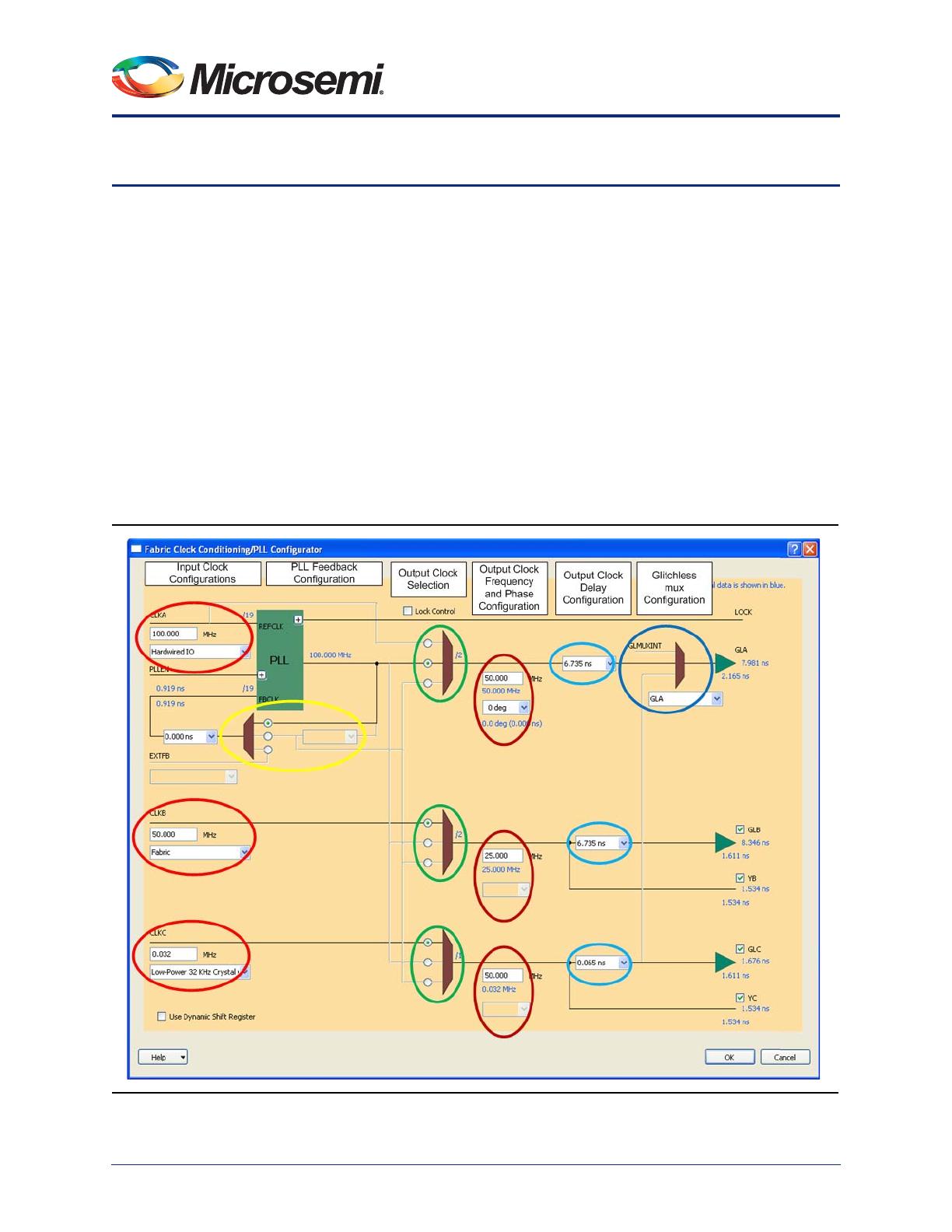
•Clock Frequency - You must specify the output clock frequencies. This frequency is used by the
FAB_CCC configuration engine to automatically compute the CCC dividers to meet your
frequency requirements. The dividers are highlighted in blue (for instance /2) in the configurator
UI.
•Phase Configuration - The PLL block offers 4 phases that you can access through the phase
selection pull-down menu. The actual phases and resulting delays are highlighted in blue on the
configurator UI. The actual phase is not the same as the selected phase if the output divider is not
1 (actual_phase = selected_phase / output_divider). The actual delay is a function of the actual
phase of the PLL output (VCO).
•Delay Configuration - For GLx only, you may configure the programmable delay to further tune
the overall CLKA to GLx delays (when the PLL is used) or CLKx to GLx delays (when the bypass
mode is used) based on your system requirements. The programmable delays are typical delays.
The total delays are highlighted in blue in the configurator UI. The delays provided by the
configurator are typical delays and match those computed by SmartTime typical conditions.
PLL Feedback Clock
• PLL Feedback Source - If the you use the PLL, you can choose to use an internal or an external
feedback loop depending on your system level requirements:
– Internal feedback from VCO (phase 0) without programmable delay - This is the default
choice.
– Internal feedback from VCO (phase 0) with programmable delay - Use a fine grain
programmable delay to tune your overall CCC delays based on your system requirements.
The programmable delays are typical delays
– External I/O - The clock source can be any regular FPGA I/O. The regular FPGA I/O is routed
to the feedback clock fabric interface pin.
– Hardwired I/O - The clock source is one of three regular FPGA I/Os that has a dedicated path
to drive the feedback clock.
– Hardwired I/O (LVPECL) - The clock source is one of two regular FPGA I/Os (P side of the
LVPECL pair) that has a dedicated path to drive the feedback clock.
– Hardwired IO (LVDS) - The clock source is one of two regular FPGA I/Os (P side of the LVDS
pair) that has a dedicated path to drive the feedback clock.
– Fabric - The clock source can be any FPGA fabric logic.
• Programmable Fix Delay - You can also add a fix delay (~2 ns typical) to your feedback loop. This
delay has been defined to be about the same delay as the clock network within the FPGA (GLx to
the input of a flip-flop).
Note: When the PLL is used with an external feedback, all engine computations are based on the
assumptions that the external feedback is driven from the GLA fabric CCC output whether through
the fabric or externally to the chip. The engine also assumes a delay of 0 ns for the path from GLA
to the fabric CCC external feedback input. To have the correct delays at the system level you must
adjust the delay computation based on the actual typical external delay.
Glitchless Clock Multiplexing
You can configure the glitch less clock multiplexor as follows:
•GLA - No dynamic multiplexing is available and the GLA output comes from the CCC internal
GLA signal.
•GLA_GLC - You can make a glitchless switch between the CCC internal GLA signal and the CCC
internal GLC signal. The output of the glitchless clock multiplexor comes out on the GLA global
network.
•GLA_GLMUXINT - You can make a glitchless switch between the CCC internal GLA signal and
the FPGA fabric signal GLMUXINT. The output of the glitchless clock multiplexor comes out on
the GLA global network.