
Evaluation Board User Guide
UG-600
One Technology Way • P. O. Box 9106 • Norwood, MA 02062-9106, U.S.A. • Tel: 781.329.4700 • Fax: 781.461.3113 • www.analog.com
Evaluating the ADAU1977/ADAU1978/ADAU1979
FEATURES
For the evaluation of the ADAU1977/ADAU1978/ADAU1979
quad ADCs
Total harmonic distortion (THD) plus noise (N): −95 dB at
−1 dBFS
Signal to noise ratio (SNR): 109 dB, A weighting filter
Built-in diagnostics for microphone inputs
APPLICATIONS
Automotive
GENERAL DESCRIPTION
The E VA L-ADAU1977Z/E VAL -ADAU1978Z/E VA L -
ADAU1979Z is used for quick evaluation of the
ADAU1977/ADAU1978/ADAU1979 quad ADCs. The
evaluation board can output up to four channels of digital
output. The evaluation board requires a power supply of +5 V
for the ADAU1978 and the ADAU1979 and a power supply of
+5 V and ±20 V (optional) for testing the diagnostic features of
the ADAU1977.
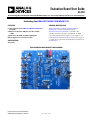
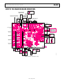
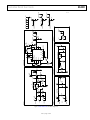
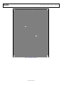
EVALUATION BOARD CONNECTION DIAGRAM
Figure 1.
11751-001
PLEASE SEE THE LAST PAGE FOR AN IMPORTANT
WARNING AND LEGAL TERMS AND CONDITIONS.
Rev. 0 | Page 1 of 27

UG-600 Evaluation Board User Guide
TABLE OF CONTENTS
Features .............................................................................................. 1
Applications ....................................................................................... 1
General Description ......................................................................... 1
Evaluation Board Connection Diagram ........................................ 1
Revision History ............................................................................... 2
Evaluation Board Hardware ............................................................ 3
Power Supply Connectors ........................................................... 3
Input Connectors .......................................................................... 3
Output Connectors ...................................................................... 3
I
2
C/SPI Control Connector ......................................................... 3
Jumpers .......................................................................................... 3
Setup of the Evaluation Board Connections ................................. 5
Evaluation Board Setup Instructions ..........................................6
Jumper Settings ..............................................................................6
USBi and Standalone GUI Setup .................................................7
ADAU1977 Power-On ..................................................................7
Standalone GUI I
2
C Control ........................................................7
Microphone Diagnostics ..............................................................8
Standalone GUI SPI Control .......................................................9
Standalone Mode ...........................................................................9
Evaluation Board Schematics and Artwork ................................ 10
Board Layout ............................................................................... 16
Ordering Information .................................................................... 23
Bill of Materials ........................................................................... 23
REVISION HISTORY
8/14—Revision 0: Initial Version
Rev. 0 | Page 2 of 27

Evaluation Board User Guide UG-600
EVALUATION BOARD HARDWARE
The E VA L-ADAU1977Z board is common for the ADAU1977,
ADAU1978, and ADAU1979. The evaluation board is designed
as a 4-layer printed circuit board (PCB). The top and bottom
layers are for signals, whereas Layer 2 and Layer 3 are used as
ground and a power plane, respectively. The PCB layout is
important to achieve good audio performance. The following
sections offer useful guidelines for operation of the board.
POWER SUPPLY CONNECTORS
The E VA L-ADAU1977Z board requires +5 V for the
ADAU1978 and ADAU1979 and may need an additional ±20 V
for testing the 10 V rms inputs of the ADAU1977. Connect the
5 V power supply at J5 and J4. Connect the ±20 V power supply
at either TP3 (+20 V) or TP1 (−20 V). The +5 V power supply
must be capable of providing a 1 A current rating, and the
±20 V power supply must be capable of providing at least a
100 mA current rating. When the diagnostics feature is not
used, the ±20 V supply is not required.
INPUT CONNECTORS
The E VA L-ADAU1977Z has five 3.5 mm audio jack connectors
for analog inputs: J9, J17, J28, J38, and J47. The J9 connector is
used for generating line level inputs capable of 10 V rms, with a
common-mode level of 7 V for the ADAU1977. The J17, J28,
J38, and J47 connectors are used as Channel 1, Channel 2,
Channel 3, and Channel 4 line level inputs to the ADC,
respectively. All five inputs are differential.
OUTPUT CONNECTORS
The ADC digital output is available at J25 (unbuffered) and J26
(buffered). In addition, ADC digital output is available as a
2-channel Sony Philips digital interface format (SPDIF). J25 and
J26 are used for I
2
S or time division multiplex (TDM), serial
digital output. The U16 provides the SPDIF optical output, and
J35 provides the SPDIF coaxial output.
I
2
C/SPI CONTROL CONNECTOR
The J8 (10-way header) can be used for I
2
C/SPI serial port
communication for controlling the board. The supplied USB
interface board can be used for setting the device. The graphic
user interface (GUI) software is used along with the USB
interface board.
JUMPERS
The EVA L-ADAU1977Z board provides jumpers for setting this
board into various operating modes.
Table 1. Jumper Descriptions
Component No. Mnemonic Description
J1 MICBIAS SELECT AUX IN This jumper allows selecting either internal or external micbias for auxiliary input.
J2 CM SELECT AUX IN Used for setting the common mode level for auxiliary input.
J4 GND Ground or 0 V connection for the power supply.
J5 +5V +5 V connection for the power supply.
J8
USBi
Connector for USBi board.
J9 AUX IN Connector for auxiliary input.
J10 IOVDD Selects the IOVDD 1.8 V or 3.3 V.
J11 IOVDD Ext/Int Selects the internal or external supply for IOVDD.
J12 VBAT Ext/Int Selects the internal or external supply for VBAT.
J13 3.3 V Ext/Int Selects the internal or external 3.3 V supply.
J14 AVDD Ext/Int Selects the internal or external AVDD supply for the ADAU1977.
J15/J20 Input 1 Select Selects the input source for Channel 1.
J16 AVDD Current This jumper is used to measure the AVDD current.
J17 CH1 Input Connector for Channel 1 input.
J19 Input Short This jumper is used to short the ± Channel 1 input.
J21 Boost Current This jumper is used to measure the boost converter current.
J22 MICBIAS-CH1 Selects the internal or external micbias for Channel 1.
J24 Boost Switch This jumper is used to measure the boost switch current.
J25 ADC Output Header for connection to ADC digital pins.
J26 ADC Output Buffered Header for ADC digital output.
J27/J30 Input 2 Select Selects the input source for Channel 2.
J28
CH2 Input
Connector for Channel 2 input.
J29 Input Short This jumper is used to short the ± Channel 2 input.
Rev. 0 | Page 3 of 27

UG-600 Evaluation Board User Guide
Component No. Mnemonic Description
J31 MICBIAS-CH1 Selects the internal or external micbias for Channel 2.
J33 IOVDD Current Connector for measuring IOVDD current.
J34 128fs Mode Selects the 96 k sample rate for the SPDIF transmitter.
J35 Coaxial Output Connector for SPDIF coaxial output.
J36/J40
Input 3 Select
Selects the input source for Channel 3
J28 CH3 Input Connector for Channel 3 input.
J39 Input Short This jumper is used to short the ± Channel 3 input.
J41 MICBIAS-CH1 Selects the internal or external micbias Channel 3.
J42 DVDD External DVDD current measurement.
J43 MCLKIN Selects the external master clock input to the ADAU1977.
J44 PLL Filter Selects the PLL filter for LRCLK mode.
J45 PLL Filter Selects the PLL filter for MCLK mode.
J46/J49 Input 4 Select Selects the input source for Channel 4.
J48 Input Short This jumper is used to short the ± Channel 4 Input.
J50 MCLKIN Selects the source for MCLKIN between oscillator, header, and Subminiature Version A,
SMA.
J51 MICBIAS-CH1 Selects the internal or external micbias Channel 4.
J52 MCLK Input SMA connector for external master clock input.
J53 FREQ Select Selects the switching frequency for the 3.3 V regulator.
JP1 AUX IN Header for external auxiliary input
JP2 CH1 IN Header for external Channel 1 input.
JP3 CH2 IN Header for external Channel 2 input.
JP4 Reset SPDIF Tx SPDIF Tx reset.
JP5 CH3 IN Header for external Channel 3 input.
JP6 SA Mode This jumper is used for standalone mode.
JP7 CH4 IN Header for external Channel 4 input.
JP8 RESET Header for the ADAU1977 reset.
JP9 MCLKIN Header for master clock input.
JP10 Reserved Reserved for internal use.
JP11 Oscillator Enable Enables the oscillator.
Rev. 0 | Page 4 of 27

Evaluation Board User Guide UG-600
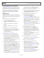
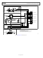
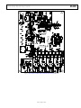
SETUP OF THE EVALUATION BOARD CONNECTIONS
Figure 2. Evaluation Board Jumper Settings
AARDVARK/USBi
SLIDE SWITCH SETTINGS
CHIP ADDRESS 0x11 ON ON
OFF
ON
ADDR1
ADDR0
256*fs
48K
I2S
MASTER
TDM4
SLOTS 1 – 4
384*fs
96K
TDM
SLAVE
TDM8
SLOTS 5 – 8
LRCLK
BCLK
SDATA2
SDATA1
SERIAL DATA OUTPUT
MASTERSLAVE
SDATA TO I2S HDR
BCLK
LRCLK
SDATA TO SPDIF OUT
BCLK
LRCLK
SDATA2
SDATA1
SDATA2
SDATA1
SDATA2
SDATA1
MCLK
+5V0V
EXT DVDD EXT IOVDDEXT AVDD
–17V TO –22V
0V
+17V TO +22V
REQUIRED ONLY
FOR GENERATING
VBAT AND 10V RMS
SIGNAL AT 7V CM
BUFFER TO BE USED FOR GENERATING
10V RMS SIGNAL AT VARIOUS CM LEVEL
GND
1/3 MICBIAS
VBAT/2
GND
2/3 MIC BIAS
VBAT/2
CM OPTIONS
AUX ANALOG INPUT
10V RMS
FAULT INPUT +INPUTS
FAULT INPUT –INPUTS
0V
CONNECT VOLTAGE SOURCE
TO INTRODUCE THE FAULT
ON INPUT 0V TO 18V MAX
NORMAL
CONTROL FOR AVDD SWITCHER
PWDN
–BUFF
–INx
+INx
ADC INPUT
SELECT
ONOFF
DIRECT COUPLE
INPUTS
NORMAL
MICBIAS
NORMAL
FAULTx
GND
GENERATE
FAULT
ON INPUTS
ON
OFF
MICBIAS
RESISTOR
SELECT
300Ω
500Ω
INT
EXT
MICBIAS
SELECT
PLL FILTER
SELECT
LRCK
MCLK
POWER
DOWN
OSCILLATOR
PSIA
OSC
SMA
MCLK
SELECT
PSIA MCLKIN
EXT MCLK
IN
DIRECT
LEVEL SHIFT
INSTALL
FOR SA MODE
DO NOT CONNECT POWER SUPPLY
INTERNAL USE ONLY
DO NOT CONNECT
POWER SUPPLY
INTERNAL USE ONLY
7 BIT DEVICE ADDRESS
ADDRESS
SETTING
FOR 0x71
ANALOG INPUT1
MAX 10V RMS
ANALOG INPUT2
MAX 10V RMS
ANALOG INPUT3
MAX 10V RMS
ANALOG INPUT4
MAX 10V RMS
+BUFF
MCLKADAU197x
SELECT
CHIP ADDRESS 0x31 ON OFF
CHIP ADDRESS 0x51 OFFON
CHIP ADDRESS 0x71 OFFOFF
STAND ALONE MODE
SPI MODE
I2CMODE
1.2MHz
600kHz
CONNECT
5V SUPPLY
11751-002
Rev. 0 | Page 5 of 27

UG-600 Evaluation Board User Guide
EVALUATION BOARD SETUP INSTRUCTIONS
To setup the EVA L-ADAU1977Z, the user needs a 5 V power
supply, differential analog input source, and a PC with a USB
port. Use a single 5 V, 1 A current rating for the power supply.
For full evaluation of the ADAU1977, a ±20 V supply is
required. This power supply facilitates the generation of a
10 V rms signal as well as a VBAT supply for microphone
diagnostics.
JUMPER SETTINGS
See Figure 2 for the setup of the evaluation board connections.
Connect the positive power supply lead to J5 and the 0 V lead to
J4 of the evaluation board. Do not turn the power supply on at
this time.
In the power supply section, take the following steps:
1. Set Jumpers J13 and J14 to the INT position.
2. Set Switch S1 to the ON position.
3. Set Jumper J10 to the desired IOVDD supply, 3.3 V, or
1.8 V.
4. Set Jumper J11 to the INT position for the internal
IOVDD.
5. Set Switch S2 to the ON position to turn on the 1.8 V
regulator.
In the daughter board section, take the following steps:
1. Install Jumpers J16, J21, J24, and J33. The J16 jumper
provides the AVDD. Jumpers J21 and J24 provide the 3.3 V
power supply to the boost converter. The J33 jumper
provides the IOVDD to the
ADAU1977/ADAU1978/ADAU1979.
In the PLL and MCLK section, take the following steps:
1. Select the master clock source. The evaluation board
provides three options for providing the master clock to
the ADC. The three options include the following: the on-
board 12.288 MHz oscillator, the external source at JP9,
and the SMA Connector J52.
2. To use the on-board oscillator, install Jumper JP11. To shut
down the oscillator, remove Jumper JP11.
3. Set Jumper J50 in the OSC center position.
4. Alternatively, if the external master clock is available, it can
either be connected at J52 as a coaxial 50 Ω SMA
connector, or at JP9 as a 2-way header (0.1” pitch). If using
JP9 as the source, install J50 in the PSIA position. If using
J52 as the source, install J50 in the SMA position.
5. The MCLK is level shifted to the required IOVDD. By default,
the level shifted master clock is used. Set Jumper J43 to the
IOVDD position. Alternatively, if direct MCLK pin access
is needed, set J43 to the 3V3 position. In this case, ensure
that the master clock supplied to the ADAU1977 is at the
correct IOVDD level.
6. Two options are provided for the PLL filter, MCLK mode
or LRCLK mode. By default, the MCLK mode is selected
by installing Jumper J44 in the MCLK position. If the
LRCLK mode is required, set J44 in the LRCLK position.
In the I
2
S output section, take the following steps:
1. Determine the serial data format used for the ADC output.
Either I
2
S/left justified (LJ)/right justified (RJ)/TDM
format or SPDIF format are available.
For I
2
S/LJ/RJ/TDM format, take the following steps:
1. Set LK3 and LK5 to the I
2
S position.
2. Set LK1 and LK2 to the I
2
S position.
3. Set Switch S13 to the MASTER position if the
ADAU1977/ADAU1978/ADAU1979 is used as a master for
the serial audio port. Alternatively, it can be set to the
SL AVE position; however, in this case, both the LRCLK
(frame clock) and the BCLK (bit clock) must be provided
from an external source.
4. The buffered serial output is available on the J26 (4-way
dual row, 0.1” pitch) header. Alternatively, the direct
(unbuffered) ADAU1977 serial outputs are available on the
J25 (8-way dual row, 0.1” pitch) header.
For SPDIF format, take the following steps:
1. Ensure LK3 and LK5 are set to the SPDIF position.
2. Ensure LK1 and LK2 are set to the SPDIF position.
3. Ensure LK4 is set to the desired serial data pair. Either
Pair 1 (Ch1 and Ch2) or Pair 2 (Ch3 and Ch4) can be
selected because only 2-channel SPDIF output is available
on the evaluation board.
4. Ensure LK6 is set to the SPDIF position which provides
the MCLK to the SPDIF transmitter.
5. The SPDIF output is available on U16 as an optical form or
on J35 as a coaxial form.
For the I
2
C/SPI control section, take the following steps:
1. Slide Switches S3, S4, and S5 are used to set the control
communication protocol for the ADAU1977.
For I
2
C protocol, take the following steps:
1. Set Switches S3, S4, and S5 to the I
2
C position.
2. Ensure JP6 is not installed.
3. The device address for the ADAU1977 is set using
Switch S9. The possible 7-bit device addresses are 0x11,
0x31, 0x51, or 0x71. The
EVA L-ADAU1977Z evaluation
board is set for the 0x71 address.
4. The 20-way (10-pin, dual row, 0.1” pitch), Shrouded
Connector J8 is used to connect the supplied USBi.
Alternatively, any other I
2
C master controller can be
connected at J8 to control the ADAU1977.
5. The Analog Devices, Inc., USBi is the quickest way to set
the EVA L-ADAU1977Z board using the supplied
standalone GUI or SigmaStudio™ software.
Rev. 0 | Page 6 of 27

Evaluation Board User Guide UG-600
For the ADAU1977 line input application, take the following
steps:
1. J9 is used to level shift the input source to the VBAT/2
level.
2. For the ADAU1977, connect the analog audio source to the
J9 auxiliary input connector.
3. J2 has two jumpers that must be set to the VBAT and
VBAT2 positions.
4. Check the dc voltage at J2 (Pin 2). This voltage should be
approximately 7 V. I f n ot , set J2 using the preset R5.
5. Set the S10, S16, S21, and S26 switches to the ON position
for dc-coupled inputs.
6. Set Jumpers J15, J20, J27, J30, J36, J40, J46, and J49 to the
BUFF position.
7. Alternatively, the signal source can be connected directly to
J17, J28, J38, and J47 by setting Jumpers J15, J20, J27, J30,
J36, J40, J46, and J49 to the –IN or +IN position. Note that
in this setting, the input source must be level shifted
appropriately.
For the ADAU1978/ADAU1979 line input applications, take the
following steps:
1. Ensure Jumper J15 and Jumper J20 are set to the –IN and
+IN position for Ch1.
2. Ensure Jumper J27 and Jumper J30 are set to the –IN and
+IN position for Ch2.
3. Ensure Jumper J36 and Jumper J40 are set to the –IN and
+IN position for Ch3.
4. Ensure Jumper J46 and Jumper J49 are set to the –IN and
+IN position for Ch4.
5. Ensure Switches S10, S16, S21, and S26 are set to the OFF
position for the ADAU1978 and the ADAU1979, which
sets the inputs as ac-coupled mode.
For the ADAU1977 microphone input application, take the
following steps:
1. Ensure Switches S7, S12, S15, S18, S20, S23, S25, and S29
are set to the ON position for using the ADAU1977 inputs
as microphone.
2. These switches are used to set the microphone bias
resistors for the microphone inputs. Either 300 Ω or 500 Ω
can be selected when switches are set to the ON position
for the respective inputs.
3. Ensure Jumpers J22, J31, J41, and J51 are set to the INT
position (the internal micbias is used). These jumpers
allow the microphone bias to be selected either from the
ADAU1977
, or externally, if desired.
4. Jumpers J17, J28, J38, and J47 are used for the microphone
input connection.
5. Ensure Jumpers J15, J20, J27, J30, J36, J40, J46, and J49 are
set to the IN position.
6. Ensure Switches S10, S16, S21, and S26 are set to the ON
position for direct-coupled mode.
USBi AND STANDALONE GUI SETUP
To set up the USBi and standalone GUI, take the following steps:
1. If using the standalone GUI, click the appropriate x86 or
x64 folder setup.exe to install the GUI.
2. The software is installed on your desktop with the
ADAU1977 Rev C icon.
ADAU1977 POWER-ON
To power-on the EVAL -ADAU1977Z, take the following steps:
1. Turn on the 5 V supply. Typical 40 mA current is drawn
from the 5 V supply in standby condition.
STANDALONE GUI I
2
C CONTROL
The E VA L-ADAU1977Z board can be controlled via the I
2
C
using the standalone GUI and USBi. Take the following steps:
1. Connect the provided USBi board to J8 and to the USB
port on the PC.
2. Double-click the ADAU1977 Rev C icon on your desktop
to invoke the GUI.
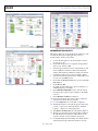
3. A new window, as is shown in Figure 3, will appear.
4. The USBi - Connected message will appear at the top of
the window (see Figure 3).
5. Click Power Up. The Communication Established
message will appear at the top of the window (see Figure 3).
6. Click Read all to read the PLL status. The PLL status
should be green and locked.
7. When using the ADAU1977, and the boost converter is
turned on, the Boost Good indicator should be green. For
the ADAU1978 and the ADAU1979, this function is not
applicable and will stay red.
8. Go to the ADC Control tab (see Figure 4) and click
Master/Slave for the ADC master mode. When green, the
ADC is in master mode and it will output the bit clock and
frame clock, together with the serial data at the J25.
9. Connect the input source at the desired input to AIN1,
AIN2, AIN3, and AIN4 or AUXIN using 3.5 mm audio
jacks. Alternatively, the 2-pin (0.1” pitch) header can be
used to feed the inputs to the EVA L-ADAU1977Z
evaluation board. Note that the input level requirements
for the ADAU1977, the ADAU1978, and the ADAU1979
are different, and the appropriate level input signal must be
applied. The full-scale inputs for the ADAU1977 is
10 V rms, for the ADAU1978 is 2 V rms, and for the
ADAU1979 is 4.5 V rms.
10. The ADC output is available at the J26 header or the SPDIF
output depending on the selected option.
Rev. 0 | Page 7 of 27

UG-600 Evaluation Board User Guide
Figure 3. Register Control for the ADAU1977 GUI Page 1
Figure 4. Register Control for the ADAU1977 GUI Page 2
Figure 5. Register Control for the ADAU1977 GUI Page 3
MICROPHONE DIAGNOSTICS
Microphone diagnostics are applicable for the ADAU1977 only,
used with the microphone input application circuit, as
described in the ADAU1977 data sheet.
1. Connect the microphone to the desired input connector:
J17, J28, J38, or J47.
2. Ensure that the inputs are dc-coupled by setting Switches
S10, S16, S21, and S26 to On.
3. Select the appropriate bias resistors using Switches S7 and
S12 for Channel 1, Switches S15 and S18 for Channel 2,
Switches S20 and S23 for Channel 3, Switches S25 and S29
for Channel 4. The resistor options are 300 Ω or 500 Ω.
4. Select the internal microphone bias by setting Jumpers J22,
J31, J41, J51 to the INT position.
5. Ensure that the Boost Good indicator is green on the GUI
Power Up tab.
6. Ensure Boost is On.
7. By default, the 48 k sample rate is selected, and the boost
switching frequency is 1.5 MHz.
8. In the MIC BIAS CONTROL section, select the desired
microphone bias output voltage (see Figure 3). By default,
it is 8.5 V.
9. Ensure Mic Bias is Enabled (see Figure 3).
10. Check the microphone bias voltage output on the EVA L -
ADAU1977Z board at the test point (TP).
11. Go to the Diagnostics tab on the GUI (see Figure 5).
12. With the microphone connected, the typical voltage at the
positive (+) input is 2/3 of microphone bias, and at the
negative (−) input is 1/3 of microphone bias.
13. Click Read in the Diagnostics tab on the GUI (see
Figure 5).
14. With proper connections and normal working conditions,
all of the channel status indicators will be blue for each
respective channel connected with the microphone.
15. To check the diagnostics functionality, create a fault situation
at the microphone input. This fault situation is done by
11751-003
11751-004
1
1751-005
Rev. 0 | Page 8 of 27

Evaluation Board User Guide UG-600
either using the microphone itself or by using the dummy
300 Ω or 500 Ω resistor connected across the positive and
negative input terminals of the evaluation board.
16. The faults are reported in the channel status indicators for
each channel for which Diag Control is Enabled (see
Figure 5).
17. The GUI shown in Figure 5 provides access to all the
diagnostics registers.
18. The DIAG TRIP POINT ADJUST1 section provides
control for adjusting the trip thresholds (see Figure 5).
19. The DIAG_ADJUST2 section provides the fault timeout
adjustment controls (see Figure 5).
20. The DIAG IRQ1 section is used to generate the IRQ using
the FAULT pin. The Fault Pin Drive section is used to
report the fault in the system (see Figure 5).
21. Use the previous controls, as well as the ADAU1977
diagnostics registers in this data sheet, to suit the needs of
the system using the intended microphone.
STANDALONE GUI SPI CONTROL
The E VA L-ADAU1977Z can also be configured for SPI control
instead of for I
2
C control. To use in SPI control mode, take the
following steps:
1. Change Slide Switches S3, S4, and S5 to SPI mode.
2. Ensure JP6 is not installed.
3. In the GUI, go to Options/Comm Protocol and select SPI
mode. (The default is I
2
C mode).
4. The evaluation board is now configured for the SPI
protocol, and the GUI functions similarly to the GUI
functions in I
2
C mode.
STANDALONE MODE
The evaluation board (EVA L -ADAU1977Z) also has a
standalone mode that does not require any I
2
C or SPI control.
In standalone mode, the ADAU1977/ADAU1978/ADAU1979
are set internally for a specific operation; no register access is
provided because the I
2
C and SPI ports are disabled. To invoke
the standalone mode (SA mode), insert Jumper JP6 and set
Slide Switches S3, S4, and S5 to the standalone position. In SA
mode, limited options are available that can be set using the
dual inline package (DIP) Switch S8. See
Table 2 for the S8
switch settings.
Table 2. Settings in SA Mode
ADAU1977 Pin No.,
Mnemonic Switch S8 Function OFF ON
Pin 17, SDA/COUT S8-6 MCLK 256 fs to 384 fs select IOVDD 384 fs GND 256 fs
Pin 18, SCL/CCLK S8-5 Full-scale (FS) 48 k/96 k select IOVDD 96 k GND 48 k
Pin 19, ADDR0/
CLATCH
S8-4 I
2
S/TDM select IOVDD TDM GND I
2
S
Pin 20, ADDR1/CIN S8-3 Master/slave select IOVDD Slave GND Master
Pin 14, SDATAOUT2 S8-2 TDM 4 to TDM 8 select IOVDD TDM 8 GND TDM 4
Pin 8, FAULT S8-1 TDM 8 slot assignments, Slot 1 to Slot 4 or
Slot 5 to Slot 8
IOVDD Slot 5 to Slot 8 GND Slot 1 to Slot 4
Rev. 0 | Page 9 of 27

UG-600 Evaluation Board User Guide
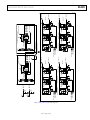
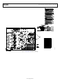
EVALUATION BOARD SCHEMATICS AND ARTWORK
Figure 6. EVAL-ADAU1977Z Schematic, Page 1 of 6
PLL FILTER SELECTION
IDVDD
DAUGHTER BOARD HEADERS
AVDD_1977
AVDD
MICBIAS
SCAN TEST HEADER
RESET ADAU1977
SELECT J44 OR J45
NORMALLY OPEN INSTALL IF USING EXT DVDD
NOTES ON JUMPER SELECTION
J21: Use for Measuring Current into DC-DC pre inductor
J24: Use for Measuring Current into DC-DC at SW node
J33: Use for measuring DUT IOVDD current
J16: Use for Measuring DUT AVDD Current
J44: PLL filter selection is using LRCLK as PLL input
J45: PLL filter selection is using MCLK as PLL input
J50: Use for selecting the level shifted MCLK for the DUT
J43: Use for selecting the direct external MCLK for the DUT
1
3
5
7
9
2
4
6
8
10
11
13
15
17
19
12
14
16
18
20
J23
2x10
1
3
5
7
9
2
4
6
8
10
11
13
15
17
19
12
14
16
18
20
J37
2x10
1
3
5
7
9
2
4
6
8
10
11
13
15
17
19
12
14
16
18
20
J32
2x10
C53
0.10µF
C65
0.10µF
C66
0.10µF
C67
0.10µF
C68
0.10µF
C61
0.10µF
C50
10µF
25V
R80
4K87
C97
39nF
C94
2.2nF NP0
1 2
L3
C39
10µF
25V
C42
0.10µF
1
3
5
7
9
2
4
6
8
10
11
13
15
17
19
12
14
16
18
20
J18
2x10
1
2
J21
DC-DC CURRENT MEASUREMENT
1
2
J16
2-JUMPER
R81
1k00
C98
5.6nF
C95
390pF
1
2
J44
PLL-LRCK
1
2
J45
PLL-MCLK
R111
OPEN
1
2
J24
CURRENT
MEASUREMENT
TP34
1
2
J33
C71
10µF
1
2
J42
C70
10µF
C49
1.0nF
+
C45
10µF
R41
OPEN
TP65
TP66
TP67
TP68
TP35
TP36
TP38
TP41
1
AGND1
2
VREF
3
PLL_FILT
4
AVDD2
5
AGND2
6
/PD/RST
7
MCLKIN
8
FAULT/TBD_SEL
9
SA_MODE
10
DVDD
11
DGND
12
IOVDD
13
SDATAOUT1
14
SDATAOUT2/TDM_SEL
15
LRCLK
16
BCLK
17
SDA/COUT/MCLK_SEL
18
SCL/CCLK/FS_SEL
19
ADDR0/CLATCH/FMT_SEL
20
ADDR1/CIN/MS_SEL
21
PGND
22
PGND
23
SW
24
SW
25
VBOOST_OUT
26
VBOOST_IN
27
MICBIAS
28
MB_GND
29
AGND3
30
VBAT
31
AVDD3
32
AIN1N
33
AIN1P
34
AIN2N
35
AIN2P
36
AIN3N
37
AIN3P
38
AIN4N
39
AIN4P
40
AVDD1
41
EPAD
U12
ADAU1977
TP43
TP44
TP46
TP47
TP74
TP71
TP55
TP54
TP42
TP40
TP29
TP28
TP23
TP50
TP24
TP25
TP63
TP61
TP27
TP69
TP45
TP57
TP72
R47
49.9Ω
R50
49.9Ω
R53
49.9Ω
R56
49.9Ω
TP73
R86
49.9Ω
L5
C106
0.10µF
JP11
R92
10.0kΩ10.0kΩ
R85
49.9Ω
C104
10pF
R83
0Ω
J52
R87
49.9Ω
C105
10pF
R90
0Ω
2
A1
3
A2
7
B1
6
B2
1
VCCA
8
VCCB
4
GND
5
DIR
U20
SN74LVC2T45DCTR
C46
0.10µF
C108
0.10µF
R78
49.9Ω
R82
10.0kΩ
1
2
JP9
R91
OPEN
R89
OPEN
1 2
3 4
5 6
J50
AB
1
2
3
J43
1
3
5
7
9
2
4
6
8
10
11
13
15
12
14
16
J25
2x8
R84
10.0kΩ
JP8
C101
0.10µF
S27
TP62
1
OE
2
GND
3
OUTPUT
4
VDD
Y1
OSC_AP3S-12.288MHZ_SMD
R130 0Ω
R131
OPEN
R132
OPEN
C111
C112
R134
10.0kΩ
1
2
J54
FAULT-PULLUP
AVDD
AVDD_ADC
IOVDD_1977
ADDR1/CIN/MS_SEL [1,5]
ADDR0/CLATCH/FMT_SEL [1,5]
SCL/CCLK/FS_SEL [5]
SDA/COUT/MCLK_SEL [5]
IOVDD
VBAT [2,4]
AIN1N
[2,6]
AIN1P
[2,6]
AIN2N
[2,6]
AIN2P
[2,6]
AIN3N
[2,6]
AIN4P
[2,6]
AIN4N
[2,6]
AIN3P
[2,6]
AVDD_ADC
[1] PD/RST_1977
[1,3] MCLKIN_1977
[5] SA_MODE
AVDD_ADC
AVDD_DC_DC
VREF
VBOOST_IN
AVDD
ADDR1/CIN/MS_SEL
ADDR0/CLATCH/FMT_SEL
SDA/COUT/MCLK_SEL
SCL/CCLK/FS_SEL
FAULT/TBD_SEL
MICBIAS_1977
SA_MODE
MCLKIN_1977
PD/RST_1977
AIN4P
AIN4N
AIN3P
AIN3N
AIN2P
AIN2N
AIN1P
AIN1N
VBAT
MICBIAS_1977 [2]
VREF
DVDD_IN
DVDD
GND
GND
GND
VREF
BCLK
LRCLK
SDATAOUT2/TDM_SEL
SDATAOUT1
BCLK_X [3]
LRCLK_X [3]
SDATAOUT2/TDM_SEL_X [3]
SDATAOUT1_X [3]
IOVDD+3.3V
MCLKIN_1977 [1,3]
+3.3V
MCLK_3.3V
+3.3V
OSC
SMA
AP
[1,3] MCLKIN_1977
[5] SDATAOUT2/TDM_SEL
[1] PD/RST_1977
SDATAOUT1
[1,5] ADDR0/CLATCH/FMT_SEL
[1,5] ADDR1/CIN/MS_SEL
LRCLK
BCLK
PD/RST_1977
[1]
IOVDD
AVDD_ADC
AVDD_ADC
AVDD_ADC
11751-006
Rev. 0 | Page 10 of 27

Evaluation Board User Guide UG-600
Figure 7. EVAL-ADAU1977Z Schematic, Page 2 of 6
INPUT CH1
MIC BIAS SELECT P
MIC BIAS SELECT N
FAULT GEN SELECT P
FAULT GEN SELECT N
AC COUPLING CAP BYPASS
SHORT P&N
INPUT CH2
MIC BIAS SELECT P
MIC BIAS SELECT N
FAULT GEN SELECT P
FAULT GEN SELECT N
AC COUPLING CAP BYPASS
SHORT P&N
INPUT CH3
MIC BIAS SELECT P
MIC BIAS SELECT N
FAULT GEN SELECT P
FAULT GEN SELECT N
AC COUPLING CAP BYPASS
SHORT P&N
INPUT CH4
MIC BIAS SELECT P
MIC BIAS SELECT N
FAULT GEN SELECT P
FAULT GEN SELECT N
AC COUPLING CAP BYPASS
SHORT P&N
OPEN
OPEN
OPEN
OPEN
OPEN
OPEN
OPEN
OPEN
INPUT BUFFER FOR LEVEL SHIFTING INPUT
ANALOG INPUTS
CM INPUT SELECT
ADJUST FOR DESIRED CM LEVEL
R106
499Ω
R108
499Ω
R105
301Ω
R107
301Ω
1
23
4
S12
1
2 3
4
S7
A B
1
2
3
J22
TP30
AB
1
2
3
J20
HDR-3WAY
AB
1
2
3
J15
HDR-3WAY
RING
SLEEVE
TIP
J17
C43
1.0nF
C37
1.0nF
1
2
JP2
1
2 3
4
S10
C40
OPEN
C36
OPEN
+
C41
10µF
+
C38
10µF
TP33
R110
499Ω
R113
499Ω
R109
301Ω
R112
301Ω
1
23
4
S18
1
2 3
4
S15
A B
1
2
3
J31
TP49
AB
1
2
3
J30
HDR-3WAY
AB
1
2
3
J27
HDR-3WAY
RING
SLEEVE
TIP
J28
C78
1.0nF
C60
1.0nF
1
2
JP3
1
2 3
4
S16
C77
OPEN
C56
OPEN
+
C74
10µF
+
C57
10µF
R115
499Ω
R117
499Ω
R114
301Ω
R116
301Ω
1
23
4
S23
1
2 3
4
S20
A B
1
2
3
J41
TP56
AB
1
2
3
J40
HDR-3WAY
AB
1
2
3
J36
HDR-3WAY
RING
SLEEVE
TIP
J38
C89
1.0nF
C85
1.0nF
1
2
JP5
1
2 3
4
S21
C88
OPEN
C84
OPEN
+
C90
10µF
+
C86
10µF
R119
499Ω
R121
499Ω
R118
301Ω
R120
301Ω
1
23
4
S29
1
2 3
4
S25
A B
1
2
3
J51
TP76
AB
1
2
3
J49
HDR-3WAY
AB
1
2
3
J46
HDR-3WAY
RING
SLEEVE
TIP
J47
C103
1.0nF
C92
1.0nF
1
2
JP7
1
2 3
4
S26
C102
OPEN
C91
OPEN
+
C100
10µF
+
C93
10µF
1
2
J19
1
2
J29
1
2
J39
1
2
J48
2
–
3
+
1
O
8
V+
4
V–
U1-A
R16
10.0kΩ
R17
10.0kΩ
+
C18
10µF
R13
100kΩ
C19
10µF
RING
SLEEVE
TIP
J9
1
2
JP1
C16
22pF
R12
10.0Ω
6
–
5
+
7
O
U1-B
R7
10.0kΩ
R9
10.0kΩ
+
C5
10µF
R8
100kΩ
C10
10µF
C6
22pF
R6
10.0Ω
R4
10.0kΩ
R3
10.0kΩ
R2
10.0kΩ
R1
10.0kΩ
CW
2
1
3
R5
1 2
3
5
7
9
11
4
6
8
10
12
J2
HEADER_12WAY_UNSHROUD
C1
C2
5
4
3
2
1
S11
C1
C2
5
4
3
2
1
S6
C1
C2
5
4
3
2
1
S17
C1
C2
5
4
3
2
1
S14
C1
C2
5
4
3
2
1
S22
C1
C2
5
4
3
2
1
S19
C1
C2
5
4
3
2
1
S28
C1
C2
5
4
3
2
1
S24
C12
0.10µF
C13
0.10µF
A B
1
2
3
J1
TP4
TP16
TP5
TP52
TP32
TP26
TP58
TP51
TP39
TP60
TP59
TP53
TP64
TP77
TP70
TP75
R122
0Ω
R123
0Ω
R124 0Ω
R125 0Ω
R126
0Ω
R127
0Ω
R128
0Ω
R129
0Ω
AIN1N
[1,6]
AIN1P
[1,6]
VBAT [2,6]
[1,2,4]
MICBIAS_CH1 [2]
MICBIAS_1977MICBIAS_EXT
MICBIAS_CH1
+OUT_BUFFER [2]
[2] –OUT_BUFFER
AIN_CH1–
AIN_CH1+
FAULT_IN+
FAULT_IN–
[2,6]
VBAT [2,6]
[1,2,4]
MICBIAS_CH1 [2]
FAULT_IN+
FAULT_IN–
[2,6]
VBAT [2,6]
[1,2,4]
MICBIAS_CH1 [2]
FAULT_IN+
FAULT_IN–
[2,6]
AIN2N
[1,6]
AIN2P
[1,6]
MICBIAS_1977MICBIAS_EXT
MICBIAS_CH2
+OUT_BUFFER [2]
–OUT_BUFFER [2]
AIN_CH2–
AIN_CH2+
AIN3N
[1,6]
AIN3P
[1,6]
MICBIAS_1977MICBIAS_EXT
MICBIAS_CH3
+OUT_BUFFER [2]
–OUT_BUFFER [2]
AIN_CH3–
AIN_CH3+
AIN4N
[1,6]
AIN4P
[1,6]
MICBIAS_1977MICBIAS_EXT
MICBIAS_CH4
+OUT_BUFFER [2]
–OUT_BUFFER [2]
AIN_CH4–
AIN_CH4+
[2]
[2]
HVDD
HVSS
[2] CM_IN+
+OUT_BUFFER [2]
+IN_BUFFER
-IN_BUFFER
[2] CM_IN–
–OUT_BUFFER [2]
MICBIAS
VBAT
[1,2,4]
CM_IN+ [2]
CM_IN– [2]
2/3MICBIAS
1/3MICBIAS
1/2VBAT
HVSS
HVDD
MICBIAS_1977MICBIAS_EXT
NOTES ON JUMPER SELECTION
J2: USE FOR SELECTING THE CM LEVEL FOR THE EXTERNAL INPUT
J1, J22, J31, J41, J51: USE FOR SELECTING INTERNAL OR EXTERNAL MICBIAS FOR INPUTS
S12, S18, S23, S29: USE FOR SELECTING THE MICBIAS RESISTOR +INPUTS
S5, S15, S20, S25: USE FOR SELECTING THE MICBIAS RESISTOR -INPUTS
J20, J15, J30, J27, J40, J36, J49, J46: USE FOR SELECTING THE DIRECT OR BUFFERED INPUT
J19, J29, J39, J48: USE FOR SHORTING THE +/- INPUT PINS FOR DIAGNOSTICS TEST
S11, S6, S17, S14, S22, S19, S28, S24: USE FOR GENERATING FAULT ON INPUT PINS FOR DIAGNOSTICS TESTING
11751-007
Rev. 0 | Page 11 of 27

UG-600 Evaluation Board User Guide
Figure 8. EVAL-ADAU1977Z Schematic, Page 3 of 6
I2S TO SPDIF
SPDIF COAX OUTPUT
SPDIF OPTICAL OUTPUT
INSTALL FOR 96KHz Fs
I2S OUTPUT
MASTER / SLAVE SELECT
SDATA1
SDATA2
LRCLK
BCLK
NC
RESET_SPDIF
NOTES ON JUMPER SELECTION
LK3, LK5: USE FOR ROUTING THE SDATA TO SPDIF OR I2S HEADER
LK2: USE FOR ROUTING THE LRCLK TO SPDIF OR I2S HEADER
LK2: USE FOR ROUTING THE BCLK TO SPDIF OR I2S HEADER
LK2: USE FOR ROUTING THE MCLK TO SPDIF
S13: USE FOR SELECTING THE I2S BUFFER AS MASTER OR SLAVE
I2S/TDM OUTPUT
14
SDIN
12
ILRCLK
13
ISCLK
21
OMCK
3
EMPH
16
CEN
1
COPY/C
28
ORIG
4
SFMT0
9
RST
6
VD
23
VL
26
TXP
25
TXN
24
H/S
19
AUDIO
10
APMS
20
HWCK0
11
TCBLD
27
HWCK1
22
GND
5
SFMT1
2
NC1
7
NC2
8
NC3
17
V
15
TCBL
18
U
U17
CS8406_HARDWARE
C107
0.10µF
C81
0.10µF
R67
47.5kΩ
R66
47.5kΩ
R61
47.5kΩ
R74
47.5kΩ
R76
47.5kΩ
R64
47.5kΩ
R73
47.5kΩ
R63
47.5kΩ
R75
47.5kΩ
R71
47.5kΩ
R60
47.5kΩ
R77
47.5kΩ
R59
47.5kΩ
R62
47.5kΩ
R72
47.5kΩ
B A
LK2
B A
LK1
B
A
LK6
B
A
LK5
B A
LK4
B
A
LK3
1
4
5
8
2
6
U19
SC937-02_AES_TRANSFORMER
1
GND
2
DVDD
3
INPUT
U16
TOTX147L(FT)
R69
243Ω
R68
110Ω
R65
10.0kΩ
L4
600Ω @ 100MHz
C73
0.10µF
J35
CTP-021A-S-YEL
C79
10nF
C87
22pF
1
2
J34
128*Fs
2
A
3
GND
1
VCCA
5
VCCY
GND
VCCA
VCCY
GND
VCCA
VCCY
GND
VCCA
VCCY
4
Y
U15
FXLP34P5X
2
A
3
1
5
4
Y
U14
FXLP34P5X
2
A
3
1
5
4
Y
U9
FXLP34P5X
2
A
3
1
5
4
Y
U18
FXLP34P5X
12
34
5
6
7
8
J26
R51
49.9Ω
C58
10pF
R37
49.9Ω
C44
10pF
R54
49.9Ω
C54
10pF
R70
49.9Ω
C82
10pF
R42
1k00
C47
100pF
R45
1k00
C52
100pF
R38
10.0kΩ
2
4
U8
NC7SZ04M5
R55
49.9Ω
R48
49.9Ω
R43
24.9Ω
R40
24.9Ω
R52
1k00
R57
1k00
C59
100pF
C64
100pF
R44
24.9Ω
R39
24.9Ω
R49
24.9Ω
R46
24.9Ω
5
A2
4
OE2
6
Y2
U11-B
9
A3
10
OE3
8
Y3
U11-C
12
A4
13
OE4
11
Y4
U11-D
2
A1
1
OE1
3
Y1
U11-A
SN74LVC125ADR
2
A
3
GND
1
OE
5
VCCY
4
Y
U13
NC7SZ125
2
A
3
GND
1
5
VCCY
4
Y
U10
NC7SZ125
7
GND
14
VCC
U11-E
SN74LVC125ADR
C80
0.10µF
C72
0.10µF
C96
0.10µF
1
2
S13
SPST_1SEC_SMD
R58
10.0kΩ
JP4
C63
0.10µF
C99
0.10µF
C17
0.10µF
C48
0.10µF
C24
0.10µF
C69
0.10µF
C26
0.10µF
C75
0.10µF
+3.3V +3.3V
+3.3V
[1] LRCLK_X
[1] SDATAOUT2/TDM_SEL_X
[1] MCLKIN_1977
+3.3V
[1] BCLK_X
[1] SDATAOUT1_X
LO
HI
+3.3V
+3.3V
IOVDD
+3.3V
IOVDD
+3.3V
IOVDD
+3.3V
+3.3V
IOVDD
SDATA1_OUT
SDATA2_OUT
BCLK_IO
LRCLK_IO
IOVDD
MASTER_SEL
[3]
SLAVE_SEL
[3]
IOVDD
IOVDD
SLAVE_SEL
[3]
IOVDD
MASTER_SEL
[3]
SDATA1_OUT
SDATA2_OUT
LRCLK_IO
BCLK_IO
1
1751-008
OE
Rev. 0 | Page 12 of 27

Evaluation Board User Guide UG-600
Figure 9. EVAL-ADAU1977Z Schematic, Page 4 of 6
HV INPUT 3.3V REG SELECT
1.8V REG SELECT IOVDD SELECT
+22VDC MAX
GND
+5VDC
+5V INPUT
–22VDC MAX
TP13TP15TP21
B
A
1
2
3
J13
TP18
TP17
C30
1.0µF
C31
1.0µF
+
C32
10µF
+
C29
15µF
3
EN
2
GND
1
IN
5
OUT
4
BYP
U4
ADP1711AUJZ-1.8-R7
C33
10nF
D3
Red Diffused
R26
475R
TP2
B A
1
2
3
J10
HDR-3WAY
TP31 TP37
1
SYNC/MODE
2
FREQ
3
TRK
4
FB
5
GND
6
PGND
7
PGND
8
PGND
9
SW
10
SW
11
SW
12
PVIN
13
PVIN
14
VIN
15
EN
16
PGOOD
17
EPAD
U3
ADP2118
R10
10Ω
R11
10.0kΩ
R18
10.0kΩ
R14
2.21kΩ
1 2
L2
C28
100µF
C14
100µF
TP9
TP3
C4
0.10µF
+
C2
47µF
1
2
J4
BINDING_POST_571_BLK
D2
TP48
TP6
C11
0.10µF
+
C15
47µF
1
2
J5
BINDING_POST_571_RED
L1
100Ω @ 100MHz
TP8
TP22
R23
243Ω
C35
0.10µF
C22
0.10µF
D1
DL4001_50V_1A_DL41
R24
2.67kΩ
C34
0.10µF
D4
3
IN
1
ADJ
4
OUT1
U2
LM317BD2T
B A
1
2
3
J12
TP20
TP1
C3
0.10µF
+
C1
47µF
R25
10k0
1
2
S1
12
S2
SPST_1SEC_SMD
TP19
1
2
J7
BINDING_POST_571_RED
BA
1
2
3
J11
C9
OPEN
1
2
J3
BINDING_POST_571_RED
BA
1
2
3
J14
C7
NF
25V
TP7
1
2
J6
BINDING_POST_571_RED
C8
OPEN
C109
1µF
C110
0.10µF
BA
1
2
3
J53
+3.3V +3.3V_EXT
+5V
1.8V
1.8V
+3.3V
IOVDD_INT
+3.3V_REG
+5V
HVDD
+5V_EXT
+15V_REG
EXT_VBAT
VBAT
HVSS
IOVDD_INTIOVDD
IOVDD_EXT
+3.3V
AVDD
AVDD_EXT
DVDD_IN
+5V
DVDD_IN
11751-009
Rev. 0 | Page 13 of 27

UG-600 Evaluation Board User Guide
Figure 10. EVAL-ADAU1977Z Schematic, Page 5 of 6
USBi OR AARDVARK I2C INTERFACE
USBI_CLK
USBI_5V00
I2C LEVEL SHIFT & DUT ADDRESS
MR LINE COMES FROM USBi BOARD RESET
LEVEL SHIFT
I2C COMMUNICATION
SPI LEVEL SHIFT
I2C, SPI or STAND-ALONE MODE SELECT
I2C-SPI OR SA MODE SELECT
ADDR1
ADDR0
STAND ALONE MODE
ADDRESS
NOTES FOR JUMPERS AND SWITCHES
S3, S4, S5 ARE 3 WAY SWITCHES TO BE USED IN TANDEM FOR I2C, SPI OR SA MODE
SET ALL THREE SWITCHES TO EITHER LEFT, CENTER OR RIGHT
S8 IS USED FOR SETTING THE PIN FUNCTIONS IN SA MODE
J8: USE FOR CONNECTING THE AARDVARK I2C/SPI CONTROL ADAPTER OR USBI
1
3
5
7
9
2
4
6
8
10
J8
R21
2.43kΩ
R22
2.43kΩ
R15
10.0kΩ
TP11TP10
2
SCLA
3
SDAA
7
SCLB
6
SDAB
1
VCCA
8
VCCB
4
GND
5
EN
U6
PCA9517DP-T_I2CBUSRPT_LVLTRANS_TSSOP8
C55
C25
0.10µF
C51
0.10µF
C27
0.10µF
2
A1
3
A2
7
B1
6
B2
1
VCCA
8
VCCB
4
GND
5
DIR
U5
SN74LVC2T45DCTR
C62
0.10µF
C83
0.10µF
1
2 3
4
S9
R34
10.0kΩ
R33
10.0kΩ
R20
2k00
R19
2k00
3
1
2
4
S4-A
7
5
6
8
S4-B
3
1
2
4
S5-A
7
5
6
8
S5-B
3
1
2
4
S3-A
7
5
6
8
S3-B
JP6
R79
10.0kΩ
R32
10.0kΩ
R31
10.0kΩ
R30
10.0kΩ
R29
10.0kΩ
1
2
3
4
5
67
8
9
10
11
12
S8
R28
10.0kΩ
R27
10.0kΩ
R36
1k00
R35
1k00
2
A
3
GND
1
VCCA
5
VCCY
GND
VCCA
VCCY
4
Y
U23
FXLP34P5X
2
A
3
1
5
4
Y
U24
FXLP34P5X
C113
0.10µF
C114
0.10µF
R133
10.0kΩ
USBI_SCL [5,6]
USBI_CCLK [5]
USBI_CLATCH [5]
USBI_CIN_MOSI [5]
+3.3V
ADDR1/CIN/MS_SEL [1]
ADDR0/CLATCH/FMT_SEL [1]
SDA/COUT/MCLK_SEL [1]
SCL/CCLK/FS_SEL [1]
+3.3V
IOVDD
USBI_SCL[5,6]
USBI_SDA[5,6]
IOVDD
+3.3V
USBI_CLATCH [5]
IOVDD+3.3V
USBI_CIN_MOSI [5]
USBI_CCLK [5]
USBI_COUT_MISO [5]
IOVDD
IOVDD
USBI_COUT_MISO [5]
USBI_SDA [5,6]
SDATAOUT2/TDM_SEL [1]
FAULT/TBD_SEL [1]
SA_MODE
SA_MODE [1]
IOVDD
FMT_SEL
MCLK_SEL
TDM_SEL
TBD_SEL
FS_SEL
MS_SEL
CIN_IOVDD
CLATCH_IOVDD
SCL_IOVDD
CCLK_IOVDD
SDA_IOVDD
COUT_IOVDD
+3.3V
IOVDD
IOVDD
+3.3V
0.10µF
11751-010
Rev. 0 | Page 14 of 27

Evaluation Board User Guide UG-600
Figure 11. EVAL-ADAU1977Z Schematic, Page 6 of 6
FAULT GENERATION LOGIC CONTROL1
FAULT GENERATION LOGIC CONTROL2
INPUT CH1
INPUT CH2
INPUT CH3
INPUT CH4
SHORT AIN2P TO AIN2N
FAULT_IN– TO AIN2N
FAULT_IN+ TO AIN2P
FAULT_IN– TO AIN1N
FAULT_IN+ TO AIN1P
SHORT AIN3P TO AIN3N
FAULT_IN– TO AIN3N FAULT_IN+ TO AIN3P
SHORT AIN4P TO AIN4N
FAULT_IN– TO AIN4N FAULT_IN+ TO AIN4P
SHORT AIN1P TO AIN1N
DISABLE FAULT LOGIC
I2C ADDRESS 0x19Hex
I2C ADDRESS 0x18Hex
FAULT GENERATION FOR AUTOMATED TESTING
1
SCL
2
SDA
3
AD0
4
AD1
5
AD2
6
IO0
7
IO1
8
GND
9
IO2
10
IO3
11
IO4
12
IO5
13
IO6
14
IO7
15
RESET
16
VDD
U22
MAX7310-QSOP16
R100
10.0kΩ
R96
OPEN
R104
10.0kΩ
R103
OPEN
R101
10.0kΩ
R97
OPEN
C23
0.10µF
1
SCL
2
SDA
3
AD0
4
AD1
5
AD2
6
IO0
7
IO1
8
GND
9
IO2
10
IO3
11
IO4
12
IO5
13
IO6
14
IO7
15
RESET
16
VDD
U21
MAX7310-QSOP16
R93
OPEN
R94
10.0KΩ
R98
10.0kΩ
R102
OPEN
R95
10.0kΩ
R99
OPEN
C76
0.10µF
+
5
8
2
4
K1
+
5
8
2
4
K6
+
5
8
2
4
K5
1
IN
2
GND
3
OUT
Q1
1
IN
2
GND
3
OUT
Q6
1
IN
2
GND
3
OUT
Q5
KA
D9
KA
D10
KA
D5
+
5
8
2
4
K2
+
5
8
2
4
K8
+
5
8
2
4
K7
1
IN
2
GND
3
OUT
Q2
1
IN
2
GND
3
OUT
Q8
1
IN
2
GND
3
OUT
Q7
KA
D11
KA
D12
KA
D6
+
5
8
2
4
K3
+
5
8
2
4
K10
+
5
8
2
4
K9
1
IN
2
GND
3
OUT
Q3
1
IN
2
GND
3
OUT
Q10
1
IN
2
GND
3
OUT
Q9
KA
D13
KA
D14
K
A
D7
+
5
8
2
4
K4
+
5
8
2
4
K12
+
5
8
2
4
K11
1
IN
2
GND
3
OUT
Q4
1
IN
2
GND
3
OUT
Q12
1
IN
2
GND
3
OUT
Q11
KA
D15
KA
D16
KA
D8
TP12
TP14
C20
0.10µF
C21
0.10µF
R88
10.0kΩ
JP10
+3.3V
USBI_SCL [5,6]
USBI_SDA [5,6]
+3.3V
FAULT_AIN4P [6]
FAULT_AIN2P [6]
FAULT_AIN1P [6]
FAULT_AIN3P [6]
FAULT_AIN4N [6]
FAULT_AIN2N [6]
FAULT_AIN1N [6]
FAULT_AIN3N [6]
+3.3V
USBI_SCL [1,2]
USBI_SDA [1,2]
+3.3V
FAULT_AIN3P_AIN3N [6]
FAULT_AIN1P_AIN1N [6]
FAULT_AIN4P_AIN4N [6]
FAULT_AIN2P_AIN2N [6]
FAULT_AIN1P [6]
FAULT_AIN1N [6]
FAULT_AIN1P_AIN1N [6]
AIN1P [1,2]
AIN1N [1,2]
+3.3V
+3.3V +3.3V
FAULT_IN–
[2,6] [2,6]
FAULT_IN+
FAULT_AIN2P [6]
FAULT_AIN2N [6]
FAULT_AIN2P_AIN2N [6]
AIN2P [1,2]
AIN2N [1,2]
+3.3V
+3.3V +3.3V
FAULT_IN–
[2,6]
FAULT_IN+
[2,6]
FAULT_AIN3P [6]
FAULT_AIN3N [6]
FAULT_AIN3P_AIN3N [6]
AIN3P
[1,2]
AIN3N
[1,2]
+3.3V
+3.3V +3.3V
FAULT_IN–
[2,6]
FAULT_IN+
[2,6]
FAULT_AIN4P [6]
FAULT_AIN4N [6]
FAULT_AIN4P_AIN4N [6]
AIN4P
[1,2]
AIN4N
[1,2]
+3.3V
+3.3V +3.3V
FAULT_IN–
[2,6]
FAULT_IN+
[2,6]
FAULT_IN+
[2,6]
FAULT_IN–
[2,6]
+3.3V
DISABLE_FAULT_LOGIC
11751-011
Rev. 0 | Page 15 of 27


Page is loading ...
Page is loading ...
Page is loading ...
Page is loading ...
Page is loading ...
Page is loading ...
Page is loading ...
Page is loading ...
-
 1
1
-
 2
2
-
 3
3
-
 4
4
-
 5
5
-
 6
6
-
 7
7
-
 8
8
-
 9
9
-
 10
10
-
 11
11
-
 12
12
-
 13
13
-
 14
14
-
 15
15
-
 16
16
-
 17
17
-
 18
18
-
 19
19
-
 20
20
-
 21
21
-
 22
22
-
 23
23
-
 24
24
-
 25
25
-
 26
26
-
 27
27
-
 28
28


Analog Devices EVAL-ADAU1979 User manual
- Type
- User manual
- This manual is also suitable for
Ask a question and I''ll find the answer in the document
Finding information in a document is now easier with AI
Related papers
-
Analog Devices EVAL-ADA4523-1BRMZ User manual
-
-
Analog Devices UG-2046 User guide
-
Analog Devices EVAL-ADG1634LEBZ User guide
-
-
-
-
Analog Devices EVAL-ADR3625 User guide
-
-
Other documents
-
AMG AMG2747 and AMG2748 Installation guide
-
miniDSP miniStreamer User manual
-
Hilti Instruction 386221 User guide
-
Texas Instruments TLV320AIC3107EVM-K - User manual
-
Bull Escala S Series Service guide
-
-
-
-
-