
SERVICE MANUAL
Digital Disc Camera
IDC-1000ZE
IDC-1000ZU
(Product Code : 126 250 01)
(U.K.)
(Product Code : 126 250 03)
(U.S.A.)
(Canada)
Contents
1. iD PHOTO DISC ........................................................2
2. OUTLINE OF iD FORMAT DISC DRIVE CIRCUIT....4
3. OUTLINE OF CIRCUIT DESCRIPTION ....................9
4. DISASSEMBLY........................................................20
5. ELECTRICAL ADJUSTMENT..................................24
6. MAC ADDRESS.......................................................29
7. TROUBLESHOOTING GUIDE.................................30
The components designated by a symbol ( ! ) in this schematic diagram designates components whose value are of
special significance to product safety. Should any component designated by a symbol need to be replaced, use only the part
designated in the Parts List. Do not deviate from the resistance, wattage, and voltage ratings shown.
CAUTION : Danger of explosion if battery is incorrectly replaced.
Replace only with the same or equivalent type recommended by the manufacturer.
Discard used batteries according to the manufacturer’s instructions.
NOTE : 1. Parts order must contain model number, part number, and description.
2. Substitute parts may be supplied as the service parts.
3. N. S. P. : Not available as service parts.
Design and specification are subject to change without notice.
SX111/E, EX, U
REFERENCE No. SM5310255
FILE NO.
PRODUCT SAFETY NOTICE
IDC-1000ZEX
(Product Code : 126 250 02)
(Europe)
(General PAL area)
8. PARTS LIST.............................................................31
ACCESSORIES & PACKING MATERIALS .............31
CABINET & CHASSIS PARTS 1 .............................32
CABINET & CHASSIS PARTS 2 .............................34
CABINET & CHASSIS PARTS 3 .............................35
ELECTRICAL PARTS ..............................................36
CIRCUIT DIAGRAM (Refer to the separate volume)
CAUTION
This product utilizes a laser.
The adjustment other than those specified herein may result in hazardous radiation exposure.

– 2 –
1. iD PHOTO DISC
1-1. iD PHOTO DISC HIGH-DENSITY TECHNOLOGY
The iD Photo Disc has a diameter of 5 centimeters and yet it
can store up to 730MB of information. A laser pulse magnetic
field modulation recording method and CAD-type ultra-high
magnetic resolution method have been used to record data
at a track pitch of 0.6 µm and an extremely short mark length
of 0.235 µ, which is smaller than the spot diameter of the
laser beam.
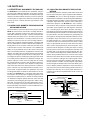
1-2. LASER PULSE MAGNETIC FIELD MODULATION
RECORDING METHOD
The beam which is generated by the laser pickup in the iD
Photo disc drive focuses onto the disc recording medium as
a spot with a diameter of about 1 µm. During recording, a
mark with a diameter of 0.235 µm -- which is smaller than the
diameter of the laser beam spot-- is recorded. A “laser pulse
magnetic field modulation” recording method has been
adopted in order to achieve this. This recording method in-
volves firstly a magnetic head which applies a magnetic field
which is modulated in accordance with the data supplied ex-
ternally which is to be recorded. In this state, the laser beam
is directed to the reverse side of the disc. The radiated light
within an 0.6 µm-diameter area at the center of the beam
spot is momentarily heated to a temperature of around 200
degrees. The data is then recorded by means of the resulting
change in the magnetic polarity of the recording layer. The
recording mark which is made by this pulse-type laser beam
is accurately formed in the track at a diameter of 0.6 µm. The
rotation of the disc causes each recording mark to overlap
the preceding mark at a point 0.235 µm forward of the pre-
ceding mark. As a result, the circles formed according to the
state of the laser beam move along and leaves a continuous
series of minute crescent-shaped marks 0.235 µm across.
These marks are approximately one-quarter the size of the
recording marks which are made on other media such as CDs
and MOs. The iD Photo disc is a magneto-optical disc which
records data uses the principle of applying magnetism and
temperature sumultaneously so that the recording medium
can maintain its magnetic polarity. Because of this, the data
cannnot be erased simply by placing the disc within a mag-
netic field, and moreover the recording method does not re-
sult in any changes to the physical nature of the disc. This
means that stable characteristics can be maintained for re-
spected disc writing operations.
1-3. CAD ULTRA-HIGH MAGNETIC RESOLUTION
METHOD
In order to play back the extremely small marks which have
been recorded using laser pulse magnetic field modulation,
the iD Photo disc uses a ultra-high magnetic resolution
method which incorporates CAD (Center Aperture Detection).
Ultra-high magnetic resolution is a form of technology in which
a magnetic signal taken from only the center of the spot is
extracted for playback. The iD Photo disc has a multi-lay-
ered structure which comprises a polycarbonate substrate,
upon which is the playback layer with magnetic characteris-
tics, a recording layer which stores the data, and finally a
heat dispersion layer which rapidly allows the spot which has
been heated by the laser beam to cool. When data is played
back from the disc, the laser beam which is generated by the
pickup passes through the polycarbonate substrate to reach
the playback layer, and focuses on a 1-µm spot. This play-
back layer functions as a screen to shield the recording layer
on which the data is recorded from the laser beam, so that
only a 0.6 µm diameter area at the center of the laser beam
which reaches the playback layer passes through it and is
projected onto the magnetic recording area of the recording
layer by means of an increase in temperature (window). The
recorded data can be picked up and read through this “win-
dow”, and the surrounding area is shielded. Moreover, in gen-
eral the spacing between the tracks is narrow and so signal
interference from tracks which are next to the track being read
can occur. However, CAD-type ultra- high magnetic resolu-
tion also solves this interference problem. With CAD-type ul-
tra-high magnetic resolution, only the magnetic signal which
passes throught the window at the center of the beam spot is
read, so that the playback reading area can be restricted to a
very narrow area not only in the tracking direction, but also in
the transverse direction. As a result, signal interference is
suppressed, and the spacing between the tracks can also be
made smaller.
Fig. 1
Fig. 2
recording spot
recording laser beam
disc movement direction
MO pit
0.235µm
ultra-high magnetic
resolution window
playback laser beam
disc movement direction
MO pit
0.235µm
value
temparature
distribution
recording layer
playback layer
T

– 3 –
1-4. PRML SIGNAL PROCESSING
When the data on the iD Photo disc is read, the 0.235 µm
overlapping recording marks which are made during laser
pulse magnetic field modulation recording are read through
an 0.6 µm window by means of a CAD-type ultra-high mag-
netic resolution reading method. Because this window has a
diameter of 0.6 µm, at least two or three recording marks can
be viewed through this window at any given time. With the iD
Photo disc, PRML signal processing has been adopted as
the signal processing method for this readable area. PRML
signal processing compares the signal wave pattern which is
detected when recording marks with several different pattern
types pass by the window with the signal wave pattern which
is actually obtained by the pickup in order to recreate the
data which has actually been recorded. This technology makes
it possible to accurately reproduce the recording marks which
are smaller than the window being used to read them, and if
a signal pattern which is not valid is read, then it is handled
as an error. In this way, recording and playback of data at
high densities can be couple with high data reliability.
1-5. ZCLV METHOD OF ROTATION CONTROL
A ZCLV (Zoned Constant Linear Velocity) method of rotation
control has been adopted for the iD Photo disc. The ZCLV
method increases the disc rotation speed on a zone basis in
accordance with the progression toward the center of the disc
as the speed of rotation of the disc recording surface with
respect to the pickup becomes progressively slower. The iD
Photo disc is devided into 12 bands from the outside to the
inside of the disc surface, and the rotation speed within each
band is varied within a range of 1900-3100 rpm in order to
maintain the speed of rotation of the recording surface with
respect to the pickup to a level of about 5 meters per second.
1-6. EXTERNAL CLOCK SIGNAL
The iD Photo disc uses an external clock method to gener-
ate the clock pulses which are used to regulate the timing for
reading and writing of data. With conventional methods, the
clock pulse is generated based on changes in the data being
read. However, with this external clock method, an FCM (Fine
Clock Mark) signal is created beforehand and recorded onto
the disc for use as a reference signal in order to generate the
clock pulse. The timing of this FCM signal is monitored dur-
ing reading of data in order to control the oscillation frequency
of the clock signal generator in accordance with the rotation
of the disc. The Fine Clock Mark is engraved accurately onto
the disc when the disc is manufactured, and it can then be
used as an accurate reference for stable reading and writing.

– 4 –
2-2. SENSOR CIRCUIT BOARD (MC2)
2-2-1. EXPLANATION OF OPERATION
Sensor circuit board (MC2) is the relay circuit board for the
disc write protection detection, disc setting detection switch,
the pickup location detection sensor and spindle motor con-
trol signal.
2. OUTLINE EXPLANATION OF DRIVE CIRCUIT
BOARD
2-1. MAGNETIC HEAD DRIVER CIRCUIT BOARD (MC1)
During recording, it is the driver circuit board to magnetize
toward the magnetic head.
2-1-1. EXPLANATION OF OPERATION
During recording, the data (WD_P and WD_N) from the MC3
circuit board is used to operate the large current buffer at IC801
in order to turn the FET array on and off. This is turn deter-
mines the direction of the magnetic field applied to the mag-
netic head. Also an upper limit is decided so that a magnetic
field level may not be bigger at the amplitude limitation circuit
by the data.
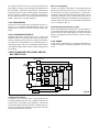
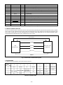
2. OUTLINE OF iD FORMAT DISC DRIVE
CIRCUIT
1. OUTLINE OF DRIVE CIRCUIT BOARD
A drive part is composed of the block diagram of the Fig. 1,
and a drive circuit board is composed of MC1, MC2 and MC3.
Fig. 1
Fig. 2
Large current
buffer
Magnetic
head
UP/DOWN
sensor
FET array
Amplitude
limitation circuit
To the
magnetic
head
WD_P
WD_N
EJULK
EJLK
+ MH+
- MH-
MC1
Amplitude
limitation circuit
To the
magnetic
head
Fig. 3
MC2
WRPROT
CARTRG
PUINI
SPDLW
SPDLU
SPDLV
SPDLCOM
Disc write protect detection switch
Disc setting detection switch
Pick up location detection sensor
S8003
S8004
D8003
To the
spindle
motor
The ascent and descent condition of the magnetic head is
being watched with the magnetic head up and down sensor.
WDTX(reverse of WDT)
WDT
(A/D) THERMO
MO signal (play signal)
(A/D) FCLKAMPL
FCLKNP
FCLKPP
FCLKZ
(A/D) ADRSAMPL
ADRSPLS
(A/D) FES
(A/D) TES
(A/D) SUM
(PWM output) FCSR
(PWM output) FCSF
(PWM output) TRKR
(PWM output) TRKF
(PWM output) SLDR
(PWM output) SLDF
SPREF
WCLK
WG
16bit
SDRAM
(64Mbit)
CPU
CAMERA
ASIC
ATA BUS
(IDE)
Processor
BUS
(TA6015F)
(BD6603KVT)
Iout
LD-ON/Off
RF-On/Off
(oscillation circuit
On/Off)
PS-On/Off(Power
saveOn/Off)
ST(abnormal
detection)
T+
T-
SLED+
SLED-
F+
F-
U/V/W/COM
A
B
C
D
E
F
G
H
I
J
A
B
C
D
Photo
sensor
output
THERMO
168
167
186
136
190
161
160
162
163
189
193
192
191
209
208
212
211
207
206
205
165
171
"0" Rec
"1" Play
50øAS-MO DRIVE CIRCUIT BOARD (MC3)
Magnetic
head
MAGNETIC HEAD
DRIVER CIRCUIT
BOARD (MC1)
DRIVE MECHA and
MECHA CIRCUIT
BOARD
iD disc(50ø)
Temparature
sensor
Pick Up
Spindle
motor
Tracking
actuator
Focus
actuator
SENSOR
BOARD
(MC2)
Laser
APC IC
(included
PICK UP)
CAMERA
DRIVE
ASIC
Sread
motor
VCC
LD
PD
RF Amplifier
FCM/ADDR
Amplifier
Servo
Amplifier
Servo
Driver
Lazer POWER
Control
CA2
SDCLK
96

– 5 –
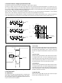
2-3. OUTLINE EXPLANATION FOR EACH BLOCK OF
DRIVE CIRCUIT BOARD (MC3)
2-3-1. SERVO AMPLIFIER
They are amplifier part for the focus servo and the tracking
servo.
1. Focus offset adjustment
When the servo and laser are both off, the DSP of the ASIC
(IC402) samples the FE (focusing error) signal and obtains
average values which are used to control the offset cancel
registers of SSI33P3721 (IC402) in order to cancel the electri-
cal offset. The signal level is set to 2.5 V DC.
2. Focus gain adjustment
The DSP of the ASIC (IC402) carries out focus searching to
measure the peak levels (+/–) for the S-shaped characteris-
tics of the FE signal, and sets the ABCD gain (focus gain) for
the SSI (IC831) in accordance with these values. The above
ABCD gain for the SSI is adjusted by the microprocessor in
order to maintain the VPP for the S-shaped characteristics of
the FE signal to approximately 1.18 V. The ABCD gain for the
SSI can be adjusted within the range of x1.2 to x4.3. During
recording (when the laser is at high power), the signal ampli-
tude is reduced by about half before the FE signal is input to
the DSP of the ASIC (IC402).
3. Focus servo ON
The DSP of the ASIC (IC402) moves the focus actuator up
and down to control the FE signal so that its AC component is
“0”.
2. TRACKING SERVO (MAIN PP AND PP SUBTRAC-
TION METHOD)
Servo control is carried out by the DSP which is built into the
ASIC (IC402). This controls the tracking actuator and the thread
actuator of the pickup in order to carry out rotation offset track-
ing control.
Fig. 4
Fig. 5
HF
C
D
B
A
E
G
IC815
BD6603KVT
IC835
(AD8532)
Buf
TES
TZC
TZC
(tracking
zero cross)
FES
PWM 5/6
TRKFTRKR
PWM 1/2
SLDF
SLDR
2
IN1F
3
IN1R
36
IN4F
35
IN4R
H1F
OUT
9
H1R
OUT
7
H4F
OUT
40
H4R
OUT
42
Tracking error signal
observation terminal
(TP811)
DSP
MACRO
IC834
(ADG702)
2.5V
WG
"0" REC
"1" PLAY
TZC
OFFSET
CANCEL
Gain-Amp
(x1~x2.2)
2x[(A+D)-(B+C)]-
α[(F+G)-(H+E)]
SSI33P3721
Gain-Amp
(±6dB)
Offset
adjustment
IC837
(AD8051)
IC814
(AD8054)
IC814
(AD8054)
IC814
(AD8054)
Main Beam PP
[(A+D)-(B+C)]
Sub Beam PP
α[(F+G)-(H+E)]
A, B, C, D
E, F, G, H
Tracking
actuator
Sread
actuator
outside
inside
Land
Land
Land
Groove
Groove
LPF
1. FOCUS SERVO (DISC SURFACE RUNOUT TRACK-
ING CONTROL)
Servo control is carried out by the DSP which is built into the
ASIC (IC402). This controls the focus actuator of the pickup in
order to carry out surface runout tracking control.
C
D
B
A
IC815
BD6603KVT
IC835
(AD8532)
Gain-Amp
Read (x1.22)
Write (x0.76)
FES
FES
PWM 3/4
FCSF FCSR
4
IN2F
5
IN2R
H2F
OUT
14
H2R
OUT
12
Focus error singal
observation terminal
(TP810)
DSP
MACRO
IC833
(ADG702)
2.5V
WG
"0" REC
"1" PLAY
OFFSET
CANCEL
Gain-Amp
(x1.4)
FES Matrix
[Kf(A+C)-(B+D)]
IC831
SSI33P3721
A, B, C, D
Focus
actuator
outside
inside
Land
Land
Land
Groove
Groove
AGC on/off
DRIVE ASIC
The S-shaped curve amplitude of the focus error signal
(FE signal) is TYP 1.2Vp-p
Minute
amplitude
2.5V
GND
The OA amplifiers and power supply
of the analog switches are all 5V.
AGC

– 6 –
1. Tracking offset adjustment
When the servo and laser are both off, the DSP of the ASIC
(IC402) samples the TE (tracking error) signal in order to con-
trol the offset cancel of SSI33P3721 (IC831) in order to can-
cel the electrical offset.
2. Tracking gain adjustment
When the focus servo is on, the DSP of the ASIC (IC402)
measures the amplitude of the TE signal and uses it to set
the CGA amp gain of the SSI (IC831).
3. Balance adjustment of main PP and sub PP
This measures the DC offset when shifting to the inside and
to the outside occurs, with respect to the center of the TE
signal when the actuator is shifted 0.83 V to the outside, when
it is shifted 0.83 V to the inside and when it is at the standard
position.
4. Servo ON (disc rotation offset tracking)
The DSP of the ASIC (IC402) moves the tracking actuator to
the left or right to control the TE signal so that its AC compo-
nent is “0”.
2-3-2. FCM/ADDR AMPLIFIER
1. FCM AMPLIFIER
FCM is an abbreviation for Fine Clock Mark. This is used as
the external clock reference to generate the signal which be-
comes the syncronizing standard for the drive circuit board.
Fig. 6
2. FCLKPP/FCLKNP/FCLKZ
These are generated from the FCM signal by the comparator
(IC852) according to the timing shown in Fig. 7.
1. When LAND is on, the lead channel macro of the ASIC
judges that a FCM has been detected after the FCLKPP
signal has been detected and the FCLKZ signal is rising.
2. When GROOVE is on, the lead channel macro of the ASIC
judges that a FCM has been detected after the FCLKNP
signal has been detected and the FCLKZ singal is falling.
1. Fine clock mark (FCM)
A computation ((A+B)–(C+D)) is carried out on the signals
from the photosensor, after which they pass through the VCA
circuit (IC853) and LPF circuit, and then the FCM signal am-
plitudes pass through the peak hold and bottom hold circuits
and are input to the DSP of the ASIC (IC402), where A/D
conversion is carried out. At the DSP of the ASIC (IC402), the
D/A value of the signal (FCLKGC) which has had the control
voltage adjusted by the VCA (IC853) is changed so that the
FCM level is set to the level which is necessary for the
FCLKNP and FCLKPP signals to be generated. Furthermore,
DSP of the ASIC (IC402) and the above circuits set the slice
level to 50 % - 70 % of the +/– side FCM marks so that the
comparator (IC852) (FCLKPP and FCLKNP) singals do not
delay the transfer of the address signals. The above circuits
adjust the signals so that the FCM amplitude is at about the
same level when at the default recording and playback power.
Furthermore, a ratio of 60 % or more between the + side and
the – side of the FCM signal is necessary when LAND is on
and when GROOVE is on. The DSP controls the control po-
tential of the VCA (IC853) so that the Vpp of the FCM signal
is about TYP 1.7 Vp-p. Furthermore, the signal interval for
the FCM signals is 532 x 50 ns = 26.6 µs.
LAND
FCLKPP
FCLKZ
FCLKNP
GROOVE
Fig. 7
C
D
B
A
outside
inside
Land
Land
Land
Groove
Groove
TPP Matrix
[(A+B)-(C+D)]
IC814
(AD8054)
IC854
(AD8054)
IC855
(ADG701)
IC857
(AD8534)
LC
Filter
A, B, C, D
FCLKGC
VCA variable
range (± 4dB)
Ctrl
IC853
(BA7655)
LC
Filter
IC854
(AD8054)
Gain-Amp
x2
FCMK signal
obwervation
termanal
(TP808)
comparator
input allowable
value (0.8~3.6V)
gain fixing
play: x 6.356
rec: x 3.33
Attenuator
WG
"0" REC
"1" PLAY
Amp
PEAK HOLD
circuit
BOTTOM
HOLD
circuit
FCLKAMPL
FCLKAMPBTM
DSP process
ASIC
IC851
(AD8534)
IC857
(AD8534)
primary
function
circuit
primary
function
circuit
Comparator
IC852
(LT1721)
FCM-PP
160
AS-MO ASIC
FCLKPP
Comparator
IC852
(LT1721)
FCM-NP
161
FCLKNP
Comparator
IC852
(LT1721)
FCM-Z
162
FCLKSLS
FCLKSLSBTM
VC25
FCLKNP
FCLKPP
2.5V
lower slice level
upper slice level
LAND
FCM
LAND
FCM
GROOVE
2.5V
2.5V
FCLKZ
26.6[µs]
A/D
A/D
D/A
D/A
The OA amplifiers, analog switch
and the power supply of the
comparator IC are all 5V.

– 7 –
2. ADDRESS DETECTION/AMPLIFIER
Mainly the address detection of the disc and signal process in
order to detect are done.
1. Address detection
The main PP signal ((A+D)–(B+D)) at the tracking servo am-
plifier shown in Fig. 5 passes through the VCA circuit (IC853)
and the LPF circuit, after which the address peak signal is
input to the DSP of the ASIC (IC402) and A/D conversion is
then carried out. As a result, the maximum amplitude of the
address signal is detected and the control potential of the VCA
(IC853) is changed so that the amplitude of the address sig-
nal can be changed to the appropriate level. Furthermore, it is
input to the comparator (IC852) to generate the address sig-
nal. This address signal is taken up by the DC macro of the
ASIC (IC402) to be used as the frame address and track ad-
dress during recording and playback.
3. The principle of rec/play clock generated by the PLL
The clock is reproduced by the PLL with respect to the signal
which has been detected to be the FCM signal by the circuit
(primary function circuit) which generates the slice level from
the FCM signal. The frequency of the reproduced clock is 20
MHz.
4. LC filter
LC filters are located before and after the VCA (IC853). Dur-
ing recording, there is the possibility that the WCLK (20 MHz)
or other high-frequency interference can become mixed in with
the FCM signal or the address signal. These LC filters remove
almost all of the signal components which are at 20 MHz or
above, leaving just the base frequencies (2-3 MHz) for the
FCM and address signals.
5. Peak hold for FCM signal and bottom hold circuit
These circuits use the amplitude modulation of the FCM sig-
nal to hold the peak level and the bottom level of the FCM
signal at the capacity which is connected to the transistor
emitter.
Fig. 8
2-3-3. RF AMPLIFIER
RF is the data signal that it is to be read by a pickup sensor (I, J).
Fig. 9
IC838
(AD8062)
MOAGCHLD
AGCOFFH
AGC on/off
I
J
Gain-Amplifier
x 8.17
AGC
Cutoff
Boost
Programmable
Equalizer
Filter
IC836
(ADG701)
+5VA
SSI33P3721
IC832
(AD8051)
MO-RF
2.0V
1.0V
136
RF
REFTOP
REFBTM
P06
AGCOFFH
137
138
221
AS-MO ASIC
TP801
(MO observation)
I/J is bias by 2.5 V (FREF).
During AGC OFF
Gain is decided.
C
D
B
A
inside
outside
Land
Land
Land
Groove
Groove
Main Matrix
[(A+D)-(B+C)]
IC814
(AD8054)
IC854
(AD8054)
IC856
(ADG701)
IC857
(AD8534)
LC
Filter
A, B, C, D
ADRSGC
VCA
variable range
(± 4dB(min))
Ctrl
IC853
(BA7655)
LC
Filter
IC854
(AD8054)
Gain-Amp
comparator
input allowable value
(0.67~3.36V)
Gain fixing
Read: x 6.81
Write: x 3.78
Attenuator
WG
"0" REC
"1" PLAY
Amp
ADRSAMPL
189
AS-MO ASIC
A14
ADRSGC
173
A02
Comparator
IC852
(LT1721)
ADRSPLS
163
VC25
ADRSPLS
PEAK HOLD
CIRCUIT
FCLKWIN
IC859
(ADG702)
The OA amplifiers, analog switch
and the power supply of the comparator
IC are all 5V.

– 8 –
2-3-4. SERVO DRIVER
The driver circuit of spindle motor, sread motor and each ac-
tuators are accumulated inside BD6603KVT (IC815). The
spindle motor is used three aspect sensorless motor (DC
motor).
2-3-5. LASER POWER CONTROL
TA6015F (optical disc power control (LPC): IC841) and
TA6012F (optical disc high speed APC) are used in the pairs.
An APC IC appears on the pickup. LPC (IC841) control makes
it possible to set characteristics such as playback power, re-
cording peak power, duty, laser on/off setting and low power
consumption standby mode using the register settings of the
LPC (IC841).
can be generated from the light which is reflected back from
the disc. Because of this, high-frequency currents of 300-600
MHz are superimposed on the laser drive currnet to reduce
interference.
2-3-6. SDRAM
This is used as a WORK for ECC encoding and decoding, as
a buffer for seamless recording and playback, and as a drive
cache.
3. BLOCK DIAGRAM OF PLAY/REC AND SIG-
NAL PROCESS etc.
1. Playback clock by PLL
The playback clock (20 MHz) which is generated from the
FCLKPP/FCLKNP signals (see Fig. 7) obtained from the FCM
is played back. The spindle motor operation is controlled by
CLV (constant linear velocity) to provide a constant FCM cycle
(26.6 µs). Accodingly, the rotation becomes faster as tracking
moves toward the center of the disc.
Fig. 10
The signals from the sensors (I/J) are pre-amplified by the
gain amplifier, and then pass through the AGC/equalizer of
the SSI (IC831), and are then input to the RF signal terminal
of the ASIC (IC402). The AGC control signal (AGCOFFH) from
the ASIC (IC402) is modulated to control the on/off status of
the AGC. When the AGC is on, the wave pattern monitored at
TP801 is adjusted to a constant amplitude.
A/D
Digital
EQI
PLL
Delay
ADRS
Dec.
SH
G.C
G.C
SSI
IC
MH
APC
IC
LPC
IC
PRML
PR(1, 1)
ECC
Temparature
sensor
CPU
Off Track
Tilt Mark
Slice Level
Delay
quantity
RCLK
2T signal
DRIVE ASIC
Tap coefficient
Expectation
value
Magnetic field strength
Driver
EQ, fc, Boost
Gain
Gain
MO
FCM
Adrs
WCLK
Duty Pr Pw
2T/8T
amplitude
ratio
APC IC (on the pickup)
The APC IC functions to maintain the current detected by the
photosensor attached to the laser to a constant level. This
has the effect of canceling any fluctuations in characteristics
resulting from the semiconductor laser temparature, and any
variances in production lots, so that the laser power can be
maintained at a stable level. The ON/OFF laser high-frequency
currents, power save and laser are output open corrector from
LPC IC, and input to APC IC.
Superimposing high-frequency currents
When a high-output semiconductor laser is used, interference

– 9 –
Fig. 1-1.Optical Black Location (Top View)
Pin No.
1
Symbol
2, 3
4
5, 6, 8,
14, 16
7, 9, 12
10
11
13
15
17
18
19
V
1
V 3
NC
GND
VOUT
VDD
CSUB
VL
RG
H
1
Pin Description
Vertical register transfer clock
Vertical register transfer clock
Vertical register transfer clock
Reset gate clock
Protection transistor bias
Horizontal register transfer clock
GND
Signal output
Circuit power
Substrate clock
Substrate bias
Waveform
DC
Voltage
-8.0 V, 0 V
-8.0 V, 0 V, 15 V
-8.0 V, 0 V
15 V
12 V, 17 V
0 V, 5 V
Table 1-1. CCD Pin Description
SUB
GND
DC
0 V
Aprox. 7 V
Different from every CCD
-8 V
When sensor read-out
Fig. 1-2. CCD Block Diagram
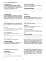
3. OUTLINE OF CIRCUIT DESCRIPTION
3-1. CA1 CIRCUIT DESCRIPTION
Around CCD block
1. IC Configuration
IC903 (ICX267) CCD imager
IC902, IC904, IC908 (74ACT04MTC) H driver
IC907 (CXD3400N) V driver
IC905 (AD9803) CDS, AGC, A/D converter
2. IC903 (CCD)
[Structure]
Interline type CCD image sensor
Optical size 1/2 type
Effective pixels 1392 (H) 1040 (V)
Pixels in total 1434 (H) 1050 (V)
Actual pixels 1360 (H) 1024 (V)
Optical black
Horizontal (H) direction: Front 2 pixels, Rear 40 pixels
Vertical (V) direction: Front 8 pixels, Rear 2 pixels
Dummy bit number Horizontal : 20 Vertical : 3
V
2A, V 2B
Pin 1
2
8
40
2
H
V
Pin 11
10
9 6 5 4 3 2 1
13
14 15 16 17
18
19
20
G
R
G
R
G
R
B
G
B
G
B
G
G
R
G
R
G
R
B
G
B
G
B
G
Vertical register
Horizontal register
Note
Note: Photo sensor
VOUT
GND
NC
NC
V
ø3
øSUB
NC
C
SUB
NC
V
L
øRG
12
GND
11
VDD
7
GND
8
NC
V
ø2B
Vø2A
Vø1
Hø1
Hø2
20
H
2
Horizontal register transfer clock
0 V, 5 V
DC
Different from every CCD

– 10 –
1A
1
1Y
2
2A
3
2Y
4
3A
5
3Y
6
GND
7
4Y
8
4A
9
5Y
10
5A
11
6Y
12
6A
13
V
CC
14
Fig. 1-3. IC902, IC904 and IC908 Block Diagram
Fig. 1-4. IC907 Block Diagram
3. IC902, IC904, IC908 (H Driver) and IC907 (V Driver)
An H driver and V driver are necessary in order to generate
the clocks (vertical transfer clock, horizontal transfer clock
and electronic shutter clock) which driver the CCD.
IC902, IC904 and IC908 are inverter IC which drives the hori-
zontal CCDs (H1 and H2). In addition the XV1-XV3 signals
which are output from IC102 are the vertical transfer clocks,
and the XSG1 and XSG signal which is output from IC102 is
superimposed onto XV2A and XV2B at IC907 in order to gen-
erate a ternary pulse. In addition, the XSUB signal which is
output from IC102 is used as the sweep pulse for the elec-
tronic shutter, and the RG signal which is output from IC102
is the reset gate clock.
4. IC905 (CDS, AGC Circuit and A/D Converter)
The video signal which is output from the CCD is input to Pin
(30) of IC905. There are S/H blocks inside IC905 generated
from the XSHP and XSHD pulses, and it is here that CDS
(correlated double sampling) is carried out.
After passing through the CDS circuit, the signal passes
through the AGC amplifier. It is A/C converted internally into
a 10-bit signal, and is then input to IC102 of the CA2 circuit
board. The gain of the AGC amplifier is controlled by serial
data which is output from IC102 of the CA2 circuit board.
Fig. 1-5. IC905 Block Diagram
SHT
V3B
V
L
V3A
V
H
V1B
V1A
GND
V4
V2
XV2
V
DD
XSHT
XSG3B
XSG3A
XV1
XSG1B
XSG1A
XV4
Input
Buffer
XV3
CCDIN
CLPDM
AUX1IN
AUX2IN
SDATA
SCK
SL
SEN
DATA
CLK
SHDSHP
DVSS
DVDD
VRT
VRB
DRVDD
DRVSS
DOUT
CLPOB
AVSS
AVDD
PBLK
CLP
2:1
MUX
BUF
CLP
CONTROL
REGISTERS
DIGITAL
INTERFACE
CDS
2:1
MUX
10
8
VGA
INTERNAL
TIMING
INTERNAL
BIAS
BANDGAP
REFERENCE
10-BIT
ADC
CLP
4 dB
Offset
DAC
AD9840
10
2~36 dB
CML

– 11 –
Fig. 1-6. Horizontal Transfer of CCD Imager and Extraction of Signal Voltage
Fig. 1-7. Theory of Signal Extraction Operation
Reset gate pulse
12V Pre-charge drain bias PD
Direction of transfer
Voltage output
Electric
charge
H Register
Floating diffusion gate is
floated at a high impedance.
C is charged
equivalently
5. Transfer of Electric Charge by the Horizontal CCD
The transfer system for the horizontal CCD emplays a 2-phase drive method.
The electric charges sent to the final stage of the horizontal CCD are transferred to the floating diffusion, as shown in Fig. 1-6.
RG is turned on by the timing in (1), and the floating diffusion is charged to the potential of PD. The RG is turned off by the timing
in (2). In this condition, the floating diffusion is floated at high impedance. The H1 potential becomes shallow by the timing in (3),
and the electric charge now moves to the floating diffusion.
Here, the electric charges are converted into voltages at the rate of V = Q/C by the equivalent capacitance C of the floating
diffusion. RG is then turned on again by the timing in (1) when the H1 potential becomes deep.
Thus, the potential of the floating diffusion changes in proportion to the quantity of transferred electric charge, and becomes
CCD output after being received by the source follower. The equivalent circuit for the output circuit is shown in Fig. 1-7.
H1 H2 H1 H2 H1 HOG RG
CCD OUT
PD
Floating diffusion
(1)
H1 H2 H1 H2 H1 HOG RG
CCD OUT
PD
(2)
H1 H2 H1 H2 H1 HOG RG
CCD OUT
(3)
H1
H2
RG
CCD OUT
3.5V
0V
3.5V
0V
15.5V
12V
Black level
RG pulse peak signal
Signal voltage
(1) (2) (3)
6. Lens drive block
6-1. Shutter drive
The shutter drive signal (SHUTTER) which is output by the
ASIC and the aperture enable signal (AE SW) cause a posi-
tive and negative voltage are applied to the aperture drive coil
to open and close the lens aperture.
6-2. Iris drive
When in the aperture enable (AE SW) state, the target aper-
ture value signal (IRIS PWM) which is output by the ASIC and
the aperture value signal (HALL OUT +/–) which is output by
the lens are compared so that feedback control can be carried
out.
6-3. Focus drive
When the drive signals (FRSTB, FCW, FOEB and FCLK) which
are output from the ASIC, the focus stepping motor is sine-
wave driven by the micro-step motor driver (IC953). Detection
of the standard focusing positions is carried out by means of
the photointerruptor (FOCUS PI) inside the lens block.
6-4. Zoom drive
When the drive signals (ZRSTB, ZCW, ZOEB and ZCLK) which
are output from the ASIC, the zoom stepping motor is sine-
wave driven by the micro-step motor driver (IC954). Detection
of the zoom positions is carried out by means of photoreflector
(ZOOM PI) inside the lens block.
6-5. ND filter drive
When the drive signals (ND ON, ND OFF) which are output
from the ASIC, ND filter opens and closes.

– 12 –
3-2. CA2 CIRCUIT DESCRIPTION
1. Circuit Description
1-1. Scannning converter (Interlace converter)
This circuit uses the function of a 64-Mbit SDRAMs to con-
vert the non-interlaced signal which is output from the CCD
into an interlaced signal for the video monitor.
1-2. Camera signal processor
This comprises circuits such as the digial clamp circuit, white
balance circuit, circuit, color signal generation circuit, ma-
trix circuit and horizontal aperture circuit.
1. Digital clamp circuit
The optical black section of the CCD extracts 16-pixel aver-
aged values from the subsequent data to make the black level
of the CCD output data uniform for each line. The 16-pixel
averaged value for each line is taken as the sum of the value
for the previous line multiplied by the coefficient k and the
value for the current line multiplied by the coefficient 1-k.
2. White balance circuit
This circuit controls the white balance by using the AWB judge-
ment value computed by the CPU to control the gain for each
R, G and B pixel based on the CCD data which has been
read.
3. circuit
This circuit performs (gamma) correction in order to maintain
a linear relationship between the light input to the camera
and the light output from the picture screen.
4. Color generation circuit
This circuit converts the CCD data into RGB signals.
5. Matrix circuit
This circuit generates the Y signals, R-Y signals and B-Y sig-
nals from the RGB signals.
6. Horizontal aperture circuit
This circuit is used generate the aperture signal.
1-3. SDRAM controller
This circuit outputs address, RAS, CAS and AS data for con-
trolling the SDRAM. It also refreshes the SDRAM.
1-4. PIO
The expansion parallel port can be used for functions such
as stroboscope control and LCD driver control.
1-5. SIO (Serial control)
This is the interface for the 4-bit microprocessor.
1-6. USB control
This is comunicated PC with 12 Mbps.
1-7. TG, SG block
This is the timing generation circuit which generates the clocks
(vertical transfer clock and electronic shutter clock) which drive
the CCD.
1-8. 8-bit D/A circuit (Audio)
This circuit converts the audio signals (analog signals) from
the microphone to 8-bit digital signals.
1-9. 8-bit A/D circuit (Audio)
The audio signals which were converted to digial form by the
8-bit A/D circuit are temporarily to a sound buffer and then
recorded in the SSFDC card. During playback, the 8-bit D/A
circuit converts these signals into analog audio signals.
1-10. Sound buffer
Audio memory
1-11. LCD driver
The Y/C signals which are input to the LCD driver are con-
verted to RGB signals, and the timing signal which is neces-
sary for LCD monitor display and the RGB signals are then
supplied to the LCD monitor.
1-12. LCD monitor
This is the image display device which displays the image
signals supplied from the LCD driver.
1-13. UART
This circuit is used for transmitting serial data to a PC. The
interface is RS-232C-compatible.
1-14. MJPEG compression
Still and continuous frame data is converted to JPEG format,
and movie images are compressed and expanded in MJPEG
format.
2. Outline of Operation
When the shutter opens, the reset signals, TEST0, TEST1
and the serial signals (“take a picture” commands) from the
8-bit microprocessor are input and record operation starts.
When the TG drives the CCD, picture data passes through
the A/D and is then input to the ASIC as 10-bit data. This data
then passes through the DCLP, AWB, shutter and circuit,
after which it is input to the SDRAM. The AWB, shutter,
and AGC value are computed from this data, and in case of
1-4 times exposures are made to obtain the optimum picture.
The data which has already been stored in the SDRAM is
read by the CPU and color generation is carried out. Each
pixel is interpolated from the surrounding data as being ei-
ther R, G or B primary color data to produce R, G and B data.
At this time, correction of the lens distortion which is a char-
acteristic of wide-angle lenses is carried out. Aperture cor-
rection is carried out, and in case of still picture the data is
then compressed by the JPEG method and in case of picture
it is compressed by MJPEG method and is transfered to MC3
block. And then it is written to iD photo disc. When the data is
to be output to an external device, it is read JPEG picture
data from the iD photo disc and output to PC via the USB or
IEEE1394.

– 13 –
3. LCD Block
During EE, gamma conversion is carried out for the 10-bit
RGB data which is input from the A/D conversion block of the
CCD to the ASIC in order that the revised can be displayed
on the video. The YUV of 640 x 480 is then transferred to the
SVRAM.
The data which has accumulated in the SDRAM is after D/A
conversion is carried out by SDRAM control circuit inside the
ASIC, makes Y/C signal, the data is sent to the LCD panel
and displayed.
If the shutter button is pressed in this condition, the 10-bit
data which is output from the A/D conversion block of the
CCD is sent to the SDRAM (DMA transfer), and is displayed
on the LCD as a freeze-frame image.
During playback, the JPEG image data which has accumu-
lated in the iD photo disc is converted to RGB signals. In the
same way as for EE, the data is then sent to the SDRAM,
after which D/A conversion is carried out inside the ASIC,
and then the data is sent to the LCD panel and displayed.
The LCD driver is converted Y/C signals to RGB signals from
ASIC, and these RGB signals and the control signal which is
output by the LCD driver are used to drive the LCD panel.
The RGB signals are 1H transposed so that no DC compo-
nent is present in the LCD element, and the two horizontal
shift register clocks drive the horizontal shift registers inside
the LCD panel so that the 1H transposed RGB signals are
applied to the LCD panel.
Because the LCD closes more as the difference in potential
between the VCOM (common polar voltage: fixed at DC) and
the R, G and B signals becomes greater, the display becomes
darker; if the difference in potential is smaller, the element
opens and the LCD become brighter. In addition, the bright-
ness and contrast settings for the LCD can be varied by means
of the serial data from the ASIC.

– 14 –
3-3. PW1 POWER CIRCUIT DESCRIPTION
1. Outline
This is the PW1 power circuit for camera block. The oscilla-
tion frequency is 400 kHz, and it has no voltage adjustment.
1-1. IC501 and IC511
This is necessary for controlling the power supply for a PWM-
type switching regulator, and IC501 is provided with four built-
in channels step-down circuits. IC511 is provided with trans-
former control and step-up circuit for backlight. The oscilla-
tion frequency is approx. 200 kHz.
1-2. Short-circuit protection circuit
If output is short-circuited for the length of time (approx. 120
ms) determined by the condenser which are connected to
Pin (17) of IC501 and Pin (17) of IC511, all output is turned
off. The control signal (P ON) are recontrolled or reset on the
power to restore output.
1-3. Head 4 V Power Output
IC501 CH1 is output. It is used for head power supply of disc.
Feedback for output voltage is provided to Pin (29) of IC501
so that PWM control can be carried out.
1-4. Digital 3.3 V System Power Output
IC501 CH2 is output. It is used for digital circuit power supply
of camera. Feedback for output voltage is provided to Pin
(26) of IC501 so that PWM control can be carried out.
1-5. Digital 2.4 V System Power Output
IC501 CH3 is output. It is used for core power supply of cam-
era ASIC. Feedback for output voltage is provided to Pin (11)
of IC501 so that PWM control can be carried out.
1-6. Motor 5 V Power Output
IC501 CH4 is output. It is used for lens circuit power supply.
Feedback for output voltage is provided to Pin (7) of IC501
so that PWM control can be carried out.
1-7. CCD Power Output
IC511 CH1 is output. It is output CCD power supply (5.1 V
(A), 15.0 V (A), –8 V (A)) and digital 5.1 V (D) by transformer
T5101. Feedback for 5.1 V (D) is provided to Pin (29) of IC511
so that PWM control can be carried out.
1-8. LCD Panel Power Output
IC511 CH2 is output. It is output LCD panel power supply
(5.1 V (L), 12.4 V (L), 15 V (L)) by transformer T5102. Feed-
back for 5.1 V (L) is provided to Pin (26) of IC511 so that
PWM control can be carried out.
1-9. EVF Back Light Power Output
IC511 CH3 is output. It is output EVF backlight power supply.
The backlight is controlled constant current 15 mA. Output
voltage is approx. 11-14 V by LED VF is scattered.
1-10. LCD Back Light Power Output
IC511 CH4 is output. It is output EVF backlight power supply.
The backlight is controlled constant current 8.3 mA. Output
voltage is approx. 20-24 V by LED VF is scattered.

– 15 –
3-4. PW2 POWER CIRCUIT DESCRIPTION
1. Outline
This is the PW2 power circuit for iD disc drive. The oscillation
frequency is 400 kHz, and it has no voltage adjustment.
1-1. IC521
This is necessary for controlling the power supply for a PWM-
type switching regulator, and is provided with four built-in chan-
nels step-down circuits. The oscillation frequency is approx.
400 kHz.
1-2. Short-circuit protection circuit
If output is short-circuited for the length of time (approx. 120
ms) determined by the condenser which is connected to Pin
(17) of IC501, all output is turned off. The control signal (P
ON) are recontrolled or reset on the power to restore output.
1-3. 4.9 V System Power Output
CH1 is output. It is divided 4.9 V (D) and 4.9 V (A). 4.9 V (A)
is mainly used for laser power supply. Feedback for output
voltage is provided to Pin (29) of IC521 so that PWM control
can be carried out.
1-4. Analog 3.1 V System Power Output
CH2 is output. It is used for disc servo etc. of analog circuit
power supply. Feedback for output voltage is provided to Pin
(26) of IC521 so that PWM control can be carried out.
1-5. Spindle 3.35 V System Power Output
CH3 is output. It is used for spindle motor power supply. Feed-
back for output voltage is provided to Pin (11) of IC521 so
that PWM control can be carried out.
1-6. Digital 3.15 V System Power Output
CH4 is output. It is used for digital circuit power supply of
disc. Feedback for output voltage is provided to Pin (7) of
IC521 so that PWM control can be carried out.

– 16 –
3-5. ST1 STROBE CIRCUIT DESCRIPTION
1. Charging Circuit
When UNREG power is supplied to the charge circuit and the
CHG signal becomes High (3.3 V), the charging circuit starts
operating and the main electorolytic capacitor is charged with
high-voltage direct current.
However, when the CHG signal is Low (0 V), the charging
circuit does not operate.
1-1. Power switch
When the CHG signal switches to Hi, Q5406 turns ON and
the charging circuit starts operating.
1-2. Power supply filter
L5401, C5401 and C5402 constitute the power supply filter.
They smooth out ripples in the current which accompany the
switching of the oscillation transformer.
1-3. Oscillation circuit
This circuit generates an AC voltage (pulse) in order to in-
crease the UNREG power supply voltage when drops in cur-
rent occur. This circuit generates a drive pulse with a frequency
of approximately 50-100 kHz. Because self-excited light omis-
sion is used, the oscillation frequency changes according to
the drive conditions.
1-4. Oscillation transformer
The low-voltage alternating current which is generated by the
oscillation control circuit is converted to a high-voltage alter-
nating current by the oscillation transformer.
1-5. Rectifier circuit
The high-voltage alternating current which is generated at
the secondary side of T5401 is rectified to produce a high-
voltage direct current and is accumulated at electrolytic ca-
pacitor C5050 on the PW1 circuit board.
1-6. Voltage monitoring circuit
This circuit is used to maintain the voltage accumulated at
C5050 at a constance level.
After the charging voltage is divided and converted to a lower
voltage by R5417 and R5419, it is output to the SY1 circuit
board as the monitoring voltage VMONIT. When this VMONIT
voltage reaches a specified level at the SY1 circuit board, the
CHG signal is switched to Low and charging is interrupted.
2. Light Emission Circuit
When RDY and TRIG signals are input from the ASIC expan-
sion port, the stroboscope emits light.
2-1. Emission control circuit
When the RDY signal is input to the emission control circuit,
Q5409 switches on and preparation is made to let current
flow to the light emitting element. Moreover, when a STOP
signal is input, the stroboscope stops emitting light.
2-2. Trigger circuit
When a TRIG signal is input to the trigger circuit, D5405
switches on, a high-voltage pulse of several kilovolts is gen-
erated inside the trigger circuit, and this pulse is then applied
to the light emitting part.
2-3. Light emitting element
When the high-voltage pulse form the trigger circuit is ap-
plied to the light emitting part, currnet flows to the light emit-
ting element and light is emitted.
Beware of electric shocks.

– 17 –
Pin
Signal
1
2~3
4~7
9
10
11
12
20
21
22
23~25
27
28~30
31
32~51
52~56
73
74
75
76
77
78
79
80
CHG VOL
GND
SCAN IN 0~3
AVREF
TARRY LED
GND
VSS
NOT USED
AVREF ON
GND
CHG ON
COM1~COM3
NOT USED
BIAS
VLC0~VLC2
VSS
S1~S20
NOT USED
GND
SO
SCK
IC
XOUT
XIN
I/O
I
-
I
I
O
-
-
-
O
-
O
O
-
-
-
-
O
-
-
I
I
O
O
-
O
I
Outline
Strobe charge voltage input (analog input)
GND
A/D converter standard voltage input terminal
Remote control LED L : LED light
GND
GND
-
A/D standard voltage ON/OFF signal L : ON
GND
Flash charge ON/OFF signal H : ON
Mode LCD common signal output
-
LCD motor voltage supply terminal
LCD motor voltage terminal
GND
Mode LCD segment signal output
GND
Video output cable connection detection signal H : Connection
Serial communication data input (←ASIC)
Serial communication data output (→ASIC)
Serial communication clock output (→ASIC)
Connect to VSS
Main clock oscillation terminal (4 MHz)
Main clock oscillation terminal
-
3-6. SY1 CIRCUIT DESCRIPTION
1. Configuration and Functions
For the overall configuration of the SY1 circuit board, refer to the block diagram. The configuration of the SY1 circuit board
centers around a 8-bit microprocessor (IC301).
The 8-bit microprocessor handles the following functions.
1. Operation key input, 2. Mode LCD display, 3. Clock control, 4. Power ON/OFF, 5. Storobe charge control
Key matrix input
SI
26
13~19
67 NOT USED - -
68 GND - GND
69 STROBE SW
I
Strobe pop up detection H : Pop up
8 AVDD
-
A/D converter analog power terminal
57~59
SCAN IN 4~6
I
Key matrix input
60 DC IN
I
DC adaptor insertion detection L : ON
61~63 NOT USED
-
-
64 WAKE UP
I Signal for detection of access condition to disc H : Rotation
65 NOT USED - -
66 MECHA SW
I
Detection of disc insertion & cover open/close L : Disc insertion and cover close
70 PA ON
O DC/DC converter (analog) ON/OFF signal H : ON
71 P ON
O DC/DC converter ON/OFF signal H : ON
72 MIC JACK
I
External microphone detection H : Insert microphone
See next page →
AV JACK
81
82
83
VDD
XCIN
-
I
O
Power supply terminal
Sub clock oscillation terminal (32.768 kHz)
Sub clock oscillation terminal
XCOUT

– 18 –
Fig. 4-1 Internal Bus Communication System
Table 4-2. Key Matrix table
2. Internal Communication Bus
The SY1 circuit board carries out overall control of camera operation by detecting the input from the keyboard and the condition
of the camera circuits. The 8-bit microprocessor reads the signals from each sensor element as input data and outputs this data
to the camera circuits (ASIC) or to the LCD display device as operation mode setting data. Fig. 4-1 shows the internal commu-
nication between the 8-bit microprocessor and ASIC RISC CPU circuits.
3. Key Operaiton
For details of the key operation, refer to the instruction manual.
91~94
95
96
97
98
99
100
SCAN OUT 0~3
LCD ON
ASIC TEST
ASIC RESET
ASIC TEST 1
AVSS
BATTERY
O
O
O
O
O
-
I
Key matrix output
LCD monitor power ON/OFF signal H : ON
ASIC reset signal L : Reset output
ASIC test signal
A/D converter GND power terminal
Battery voltage input (analog input)
ASIC reset control signal
Table 4-1. 8-bit Microprocessor Port Specification
89
JOG R I Jog right rotation
90
JOG L
I
Jog left rotation
0
1
2
3
1
23
SCAN
OUT
SCAN
IN
LEFT
1st
STILL IMAGE
SET
DOWN
2nd
EXE CUTE
SEQUENTIAL
SHOT
RIGHT
AF
OPT
MODE
UP
-
-
4
AE
COMMUNICA-
TION
ZOOM TELE
5
AWB
POWER
ZOOM WIDE
6
CAMERA
-
-
84
85
RESET
BAT OFF
I
I
Reset input
Battery OFF detection signal L : OFF
86
87
IR IN
SREQ
I
I
Remote control signal input terminal
Serial communication request signal L : Request
88
I
USB connector connection detection signal L : Connection
f2f1
8-bit
microprocessor
ASIC RISC CPU
1 CHIP CPU
S. REQ
RESET
ASIC SO
ASIC SI
ASIC SCK
ASIC TEST 0
ASIC TEST 1
Auto/Manual
USB
SHOOTING
VIDEO CLIPS

– 19 –
ASIC, RISC
CPU,
memory
CCD
4bit
CPU
MODE
LCD
LCD (EVF)
MONITOR
Supply voltage
Power OFF
Play back
Shutter switch ON
Resolution, Flash,
Self timer switch ON
LCD finder
3.3 V, 2.5 V
3.3V(D) 5V(A)
+15 V -8 V
3.2 V
(ALWAYS)
3.2 V
(ALWAYS)
5V (L)
+12V etc.
OFF OFF
32KHz OFF
OFF
ON
OFF
4MHz ON ON/OFF
OFF
OFF
4MHz ON OFF
ON
ON OFF
4MHz ON OFF
OFF
OFF
4MHz ON OFF
ON ON 4MHz
ON
ON/OFF
Table 4-3. Camera Mode (Battery Operation)
ASIC, RISC
CPU,
memory
CCD
4bit
CPU
MODE
LCD
LCD (EVF)
MONITOR
Supply voltage
Power OFF
Continuous image
Power switch ON-Auto power down
Take a picture
Erase image
Download image
3.3 V
5 V (A)
+15 V -8 V
3.2 V
(ALWAYS)
3.2 V
(ALWAYS)
5 V (L)
+12V etc.
OFF
OFF
32 KHz OFF OFF
OFF
OFF
4 MHz ON OFF
ON
ON OFF
4 MHz ON OFF
ON
OFF
4 MHz ON OFF
ON
OFF
4 MHz ON OFF
ON
ON
4 MHz ON OFF
Power
ON
Table 4-4. Host Mode (Battery Operation)
Message from host
ON
ON
4 MHz ON OFF
Note) P. SAVE = Power save mode, 4 MHz = Main clock operation, 32 kHz = Sub clock operation
4. Power Supply Control
The 8-bit microprocessor controls the power supply for the overall system.
The following is a description of how the power supply is turned on and off. When the battery is attached, a regulated 3.2 V
voltage is normally input to the 8-bit microprocessor (IC301) by IC302, so that clock counting and key scanning is carried out
even when the power switch is turned off, so that the camera can start up again. When the battery is removed, the 8-bit micro-
processor operates in sleep mode using the backup battery. At this time, the 8-bit microprocessor only carries out clock counting,
and waits in standby for the battery to be attached again. When a switch is operated, the 4-bit microprocessor supplies power to
the system as required.
The 8-bit microprocessor first sets both the P ON signal at pin (71) and the PA ON signal at pin (70) to high, and then turns on the
DC/DC converter. After this, Low pulse are output from pins (96), (98) and (97) in order so that the ASIC RISC CPU is set to the
active condition. If the LCD monitor is on, the LCD ON signal at pin (95) set to high, and the DC/DC converter for the LCD monitor
is turned on. Once RISC CPU processing is completed, the ASIC RISC CPU return to the reset condition, all DC/DC converters
are turned off and the power supply to the whole system is halted.
Power switch ON-Auto power down
Power
ON
DRIVE
4.9V(D),3.15V(P),
4.9V(A),3.15V(D),
4V(H), 3.1V(A)
OFF
ON
OFF
ON
OFF
ON
DRIVE
↑
OFF
OFF
ON
ON
ON
ON
ON
No disc
OFF
OFF
4MHz ON OFF
OFF
No disc
OFF
OFF
4 MHz ON
OFF OFF

– 20 –
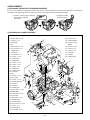
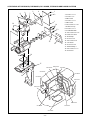
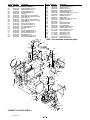
4. DISASSEMBLY
4-1. REMOVING THE PROTECTIVE SPACER AND NOTES
If the camera is dropped or subjected to other strong shocks, it may damage the mechanical pickup function. To prevent the
possibility of this happening, attach the protective spacer to the camera when transporting the camera.
4-2. REMOVAL OF CABINET ASSEMBLY
1. Three screws 1.7 x 5
2. Screws 1.7 x 4
3. Cabinet top
4. FPC
5. Two screws 1.7 x 3.5
6. Four screws 1.7 x 3
7. Cabinet lens L
8. Cabinet VF
9. Six screws 1.7 x 4
10. Screw 1.7 x 2.5
11. Cover bottom
12. Cabinet back
13. Screw 1.7 x 3.5
14. Screw 1.7 x 2.5
15. Screw 1.7 x 5
16. Cabinet front
17. Cabinet lens R
18. Connector
19. FPC
20. Screw 1.7 x 2.5
21. SY2 board
22. Screw 1.7 x 3.5
23. Flexible PWB unit
24. Two FPCs
25. Connector
26. Cabinet jog B
27. Two screws 1.7 x 2.5
28. Button AWB
29. Five screws 1.7 x 4
30. SY4 board
31. Two screws 1.7 x 4
32. Holder zoom A
33. Push the button.
34. Three screws 1.7 x 2.5
35. Screw 1.7 x 5
36. Holder flash B
37. Two screws 1.7 x 4
38. Screw 1.7 x 6
39. Cabinet bottom
40. Open the cover
battery.
41. Screw 1.7 x 2.5
42. Screw 1.7 x 5
43. Screw 1.7 x 5
44. Connector
45. Ring MF
46. Cabinet side L
A
A
C
C
D
D
B
B
38
37
39
1
1
3
4
5
6
6
7
8
9
9
10
11
12
13
1
14
15
16
9
46
36
17
18
19
20
21
22
25
26
27
28
29
30
31
32
33
34
35
40
41
42
43
44
45
23
24
2
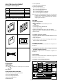
1. Push the eject lever in the direction
of the arrow to open the
disk holder.
2. Gently pull out the
protective spacer.
Page is loading ...
Page is loading ...
Page is loading ...
Page is loading ...
Page is loading ...
Page is loading ...
Page is loading ...
Page is loading ...
Page is loading ...
Page is loading ...
Page is loading ...
Page is loading ...
Page is loading ...
Page is loading ...
Page is loading ...
Page is loading ...
Page is loading ...
Page is loading ...
Page is loading ...
Page is loading ...
Page is loading ...
Page is loading ...
Page is loading ...
Page is loading ...
Page is loading ...
Page is loading ...
-
 1
1
-
 2
2
-
 3
3
-
 4
4
-
 5
5
-
 6
6
-
 7
7
-
 8
8
-
 9
9
-
 10
10
-
 11
11
-
 12
12
-
 13
13
-
 14
14
-
 15
15
-
 16
16
-
 17
17
-
 18
18
-
 19
19
-
 20
20
-
 21
21
-
 22
22
-
 23
23
-
 24
24
-
 25
25
-
 26
26
-
 27
27
-
 28
28
-
 29
29
-
 30
30
-
 31
31
-
 32
32
-
 33
33
-
 34
34
-
 35
35
-
 36
36
-
 37
37
-
 38
38
-
 39
39
-
 40
40
-
 41
41
-
 42
42
-
 43
43
-
 44
44
-
 45
45
-
 46
46


Sanyo IDC-1000ZEX iDshot User manual
- Type
- User manual
- This manual is also suitable for
Ask a question and I''ll find the answer in the document
Finding information in a document is now easier with AI
Related papers
Other documents
-
StarTech.com PLATE9MB Owner's manual
-
 Dorel Home Furnishings 3235098 Owner's manual
-
FSR PWB-320-TrK Installation guide
-
-
ESAB D3/D4 Diode Assembly Adaptor Kit Installation guide
-
Denon DBP-2012UD User manual
-
Sony MZ-R50 User manual
-
Biamp IWA250 VCA User manual
-
Haier 21F8A User manual
-
Sharp PN-HW751 Owner's manual
