5/51
Application Note
Op-Amp/Comparator Tutorial
© 2011 ROHM Co., Ltd. 64AN070E Rev.007
Jun.2021
Note: Dual power supply refers to the application of a power supply voltage to op-amps using two voltage power supplies (positive and negative).
Single power supply refers to the application of a power supply voltage to op-amps with reference to the ground.
2 Absolute Maximum Rating
The absolute maximum rating is specified in the data sheet
for op-amps/comparators. The absolute maximum rating
provides the condition that must not be exceeded even
instantaneously. The application of a voltage above the
absolute maximum rating or use in a temperature
environment outside the environment specified by the
absolute maximum rating may cause the deterioration of
characteristics or destruction of the internal circuit. The
absolute maximum ratings for the following items are
explained.
2.1. Power supply voltage/operating range of power supply
voltage
2.2. Differential input voltage
2.3. Input common-mode voltage
2.4. Input current
2.5. Operating temperature range
2.6. Maximum junction temperature, storage temperature
range
2.7. Power dissipation (total dissipation)
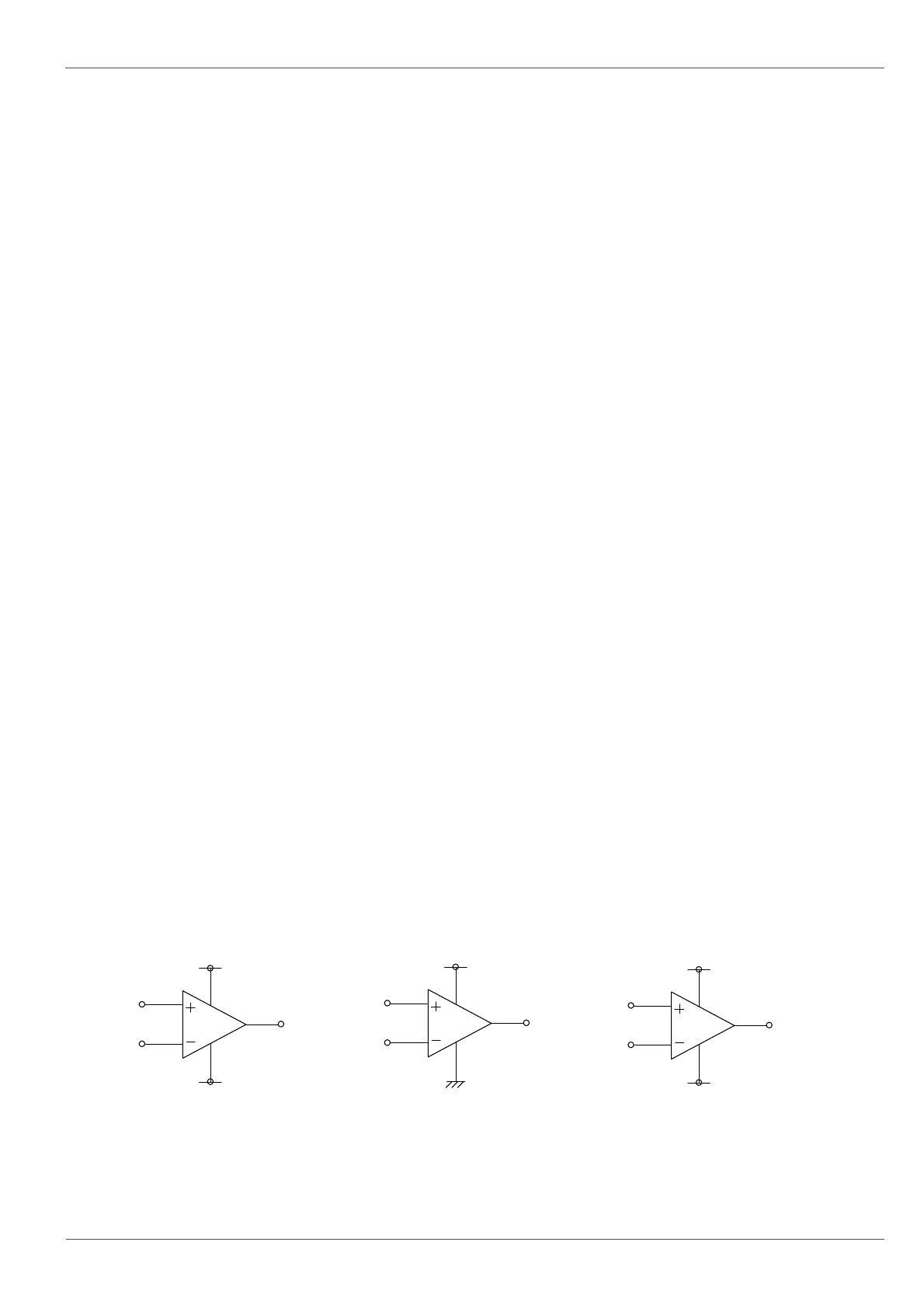
2.1 Power supply voltage/operating range of
power supply voltage
For the power supply voltage, the absolute maximum rating
refers to the maximum power supply voltage that can be
applied between the positive side power supply terminal
(VCC terminal) and the negative side power supply terminal
(VEE terminal) of the op-amp without causing the
deterioration of characteristics or destruction of the internal
circuit. Figure 2.1.1 shows examples of the power supply
voltage that can be applied to an op-amp/comparator that has
an absolute maximum rating for the power supply voltage of
36 V. The absolute maximum rating for the power supply
voltage specifies the difference in voltage between the VCC
and VEE terminals. The op-amp/comparator must be used
with the value of (VCC-VEE) never exceeding the absolute
maximum rating for the power supply voltage. Therefore,
when 24 V and -12 V are applied to the VCC and VEE
terminals, respectively, the difference in voltage between the
terminals is 36 V and the deterioration of characteristics or
destruction does not occur. It should be noted that the
absolute maximum rating for the power supply voltage has a
different meaning from the operating power supply voltage.
The absolute maximum rating for the power supply voltage
indicates the maximum value of the power supply voltage that
will not cause the characteristics deterioration or destruction
of the IC. It does not provide the voltage range in which the
specifications and characteristics that are described in the
data sheet are maintained. To obtain the characteristics that
are guaranteed in the specifications, the op-amp/comparator
must be used with the voltage value within the operating
range of the power supply voltage. However, the absolute
maximum rating for the power supply voltage of some
products may be identical to the maximum value of the
operating power supply voltage. Op-amps are sometimes
called dual power supply or single power supply op-amps. In
other words, an op-amp may be suited for the usage as a
dual power supply or single power supply. Dual power supply
op-amps have a voltage range in which either the input
voltage or the output voltage cannot be output due to the
circuit configuration on the positive power supply (VCC) side
and the negative power supply (VEE) side. Therefore, the
dual power supply op-amps are often used while applying a
positive power supply and a negative power supply with the
ground being the middle point. On the other hand, the single
power supply op-amps are used while applying the positive
power supply with reference to the ground and the
input/output can be performed nearly at the ground level.
V
OUT
VEE=-18V
VCC=18V
V
OUT
VEE=GND
VCC=36V
V
OUT
VEE=-12V
VCC=24V
VCC-VEE=18V-(18V)=36V
Dual power supply, ±18 V applied
VCC-VEE=36V-(0V)=36V
Single power supply, 36 V applied
VCC-VEE=24V-(-12V)=36V
Dual power supply, 24 V and -12 V applied
Figure 2.1.1. Examples of the power supply voltage that can be applied to an IC that has an
absolute maximum rating for the power supply voltage of 36 V


