Super Talent Technology W1333UB4GV Datasheet
- Category
- Memory modules
- Type
- Datasheet
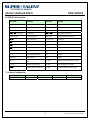
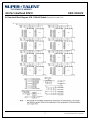
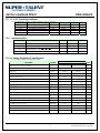
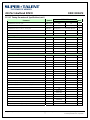
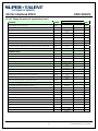
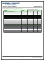
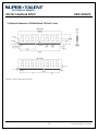
Super Talent Technology W1333UB4GV is a high-performance, unbuffered DDR3 SDRAM DIMM module designed for use in servers, workstations, and other high-end computing applications. It features a high density of 4GB, organized as 512Mx64, and operates at a speed of 1333MHz with a low voltage of 1.5V. The module is constructed using high-quality components and materials, including a TFBGA package and gold-plated contacts, to ensure reliability and durability. It is also RoHS compliant and has a wide operating temperature range of -55°C to +100°C.
Super Talent Technology W1333UB4GV is a high-performance, unbuffered DDR3 SDRAM DIMM module designed for use in servers, workstations, and other high-end computing applications. It features a high density of 4GB, organized as 512Mx64, and operates at a speed of 1333MHz with a low voltage of 1.5V. The module is constructed using high-quality components and materials, including a TFBGA package and gold-plated contacts, to ensure reliability and durability. It is also RoHS compliant and has a wide operating temperature range of -55°C to +100°C.


-
 1
1
-
 2
2
-
 3
3
-
 4
4
-
 5
5
-
 6
6
-
 7
7
-
 8
8
-
 9
9
-
 10
10


Super Talent Technology W1333UB4GV Datasheet
- Category
- Memory modules
- Type
- Datasheet
Super Talent Technology W1333UB4GV is a high-performance, unbuffered DDR3 SDRAM DIMM module designed for use in servers, workstations, and other high-end computing applications. It features a high density of 4GB, organized as 512Mx64, and operates at a speed of 1333MHz with a low voltage of 1.5V. The module is constructed using high-quality components and materials, including a TFBGA package and gold-plated contacts, to ensure reliability and durability. It is also RoHS compliant and has a wide operating temperature range of -55°C to +100°C.
Ask a question and I''ll find the answer in the document
Finding information in a document is now easier with AI
Related papers
Other documents
-
Transcend TS2GKR72V8Z Datasheet
-
-
Samsung M471B1G73AH0 User manual
-
 Elixir M2S4G64CB8HG5N-CG Datasheet
-
 Elixir M2F8G64CB8HB5N-CG Datasheet
-
 Elixir M2F4G64CB8HG5N-CG Datasheet
-
Elixir M2S8G64CB8HB5N-CG Datasheet
-
 Elixir M2F2G64CB88B7N-CG Datasheet
-
 Elixir M2F2G64CB8HA4N-CG Datasheet
-
 Elixir M2F2G64CB88DHN-CG Datasheet


